Home - douggilliland/IOP16 GitHub Wiki

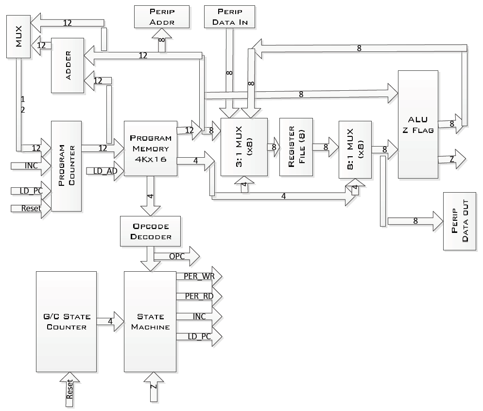
This CPU is intended to be used as an I/O Processor. The CPU can be used as a Microcontroller replacement in many applications. It implemented in an FPGA. It is useful for offloading polled I/O or replacing CPUs in small applications. The majority of these applications deal with 8-bit data and that's where this CPU excels.
- 16-bit CPU
- Simple/consistent opcode bit fields
- Instructions are always 16-bits wide
- 4-bit opcode
- Some "sub-instructions" allow more than 16 instructions
- 4-bit register field (shared with address/offset)
- 8-bit constant (shared with address/offset)
- High enough Performance - 12.5 MIPS
- 4 of 50 MHz FPGA clocks
-
Register File
- 8 General Purpose registers
- 3 constant value registers
- Registers are 8-bits
- 12-bit of Program address (up to 4K instructions)
-
Subroutine Address Stack
- 0 (none)
- 1 deep
- Optionally deeper as build option (uses SRAM)
-
Table driven Assembler
- Input comes from a CSV file
- Outputs .MIF and Listing files
- MIF (Memory Initialization File) is Altera ROM initialization File
- Targeted at an FPGA implementation
- The CPU could easily be run on pretty much any FPGA
- Coded in VHDL
- Very small LUT/Memory footprint in FPGA
- Uses 226 logic cells in an Altera EP4 FPGA
- Requires a minimum 2 of 1K SRAM blocks (depends on program size)
- Trade-off - SRAM could be replaced with logic cells (in theory)
- Very small LUT/Memory footprint in FPGA
- Uses 271 logic cells in an Altera EP4 FPGA
- Uses 76 registers in an Altera EP4 FPGA
- Requires a minimum 1 of 1K SRAM blocks (depends on program size)
- Trade-off - SRAM could be replaced with logic cells (in theory)
- The initial targeted hardware is the QMTECH EP4CE15 FPGA card
- This FPGA is inexpensive and powerful
- The CPU takes up very little of the resources of the FPGA

- QMTECH CYCLONE IV STARTER KIT GitHub
- QMTECH EP4CE15 FPGA card - AliExpress page
- Extensive Peripheral Support
- 8-bit address (controls up to 256 peripherals)
- 8-bit data
- Read strobe (a couple of clocks wide)
- Write strobe (a couple of clocks wide)