vB5 Main Board - alanbjohnston/CubeSatSim GitHub Wiki
These instructions are for the vB5 version of the CubeSatSim. Information on the latest version is here.
To assemble the boards, you will need these tools:
- Soldering iron and solder
- Hot glue gun (helpful)
- Small Philips screwdriver
- Needle nose pliers
- Wire strippers or a blade
Main Board Instructions
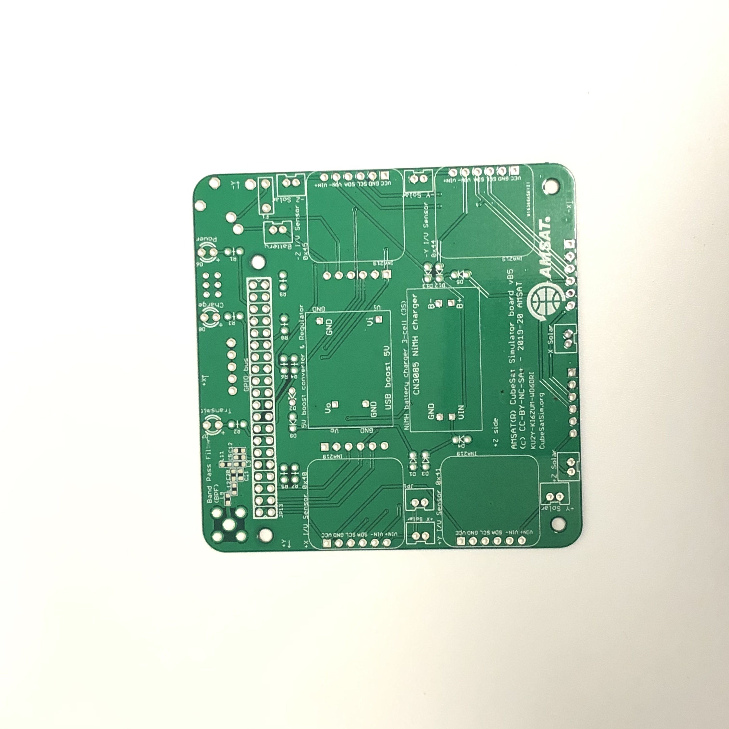
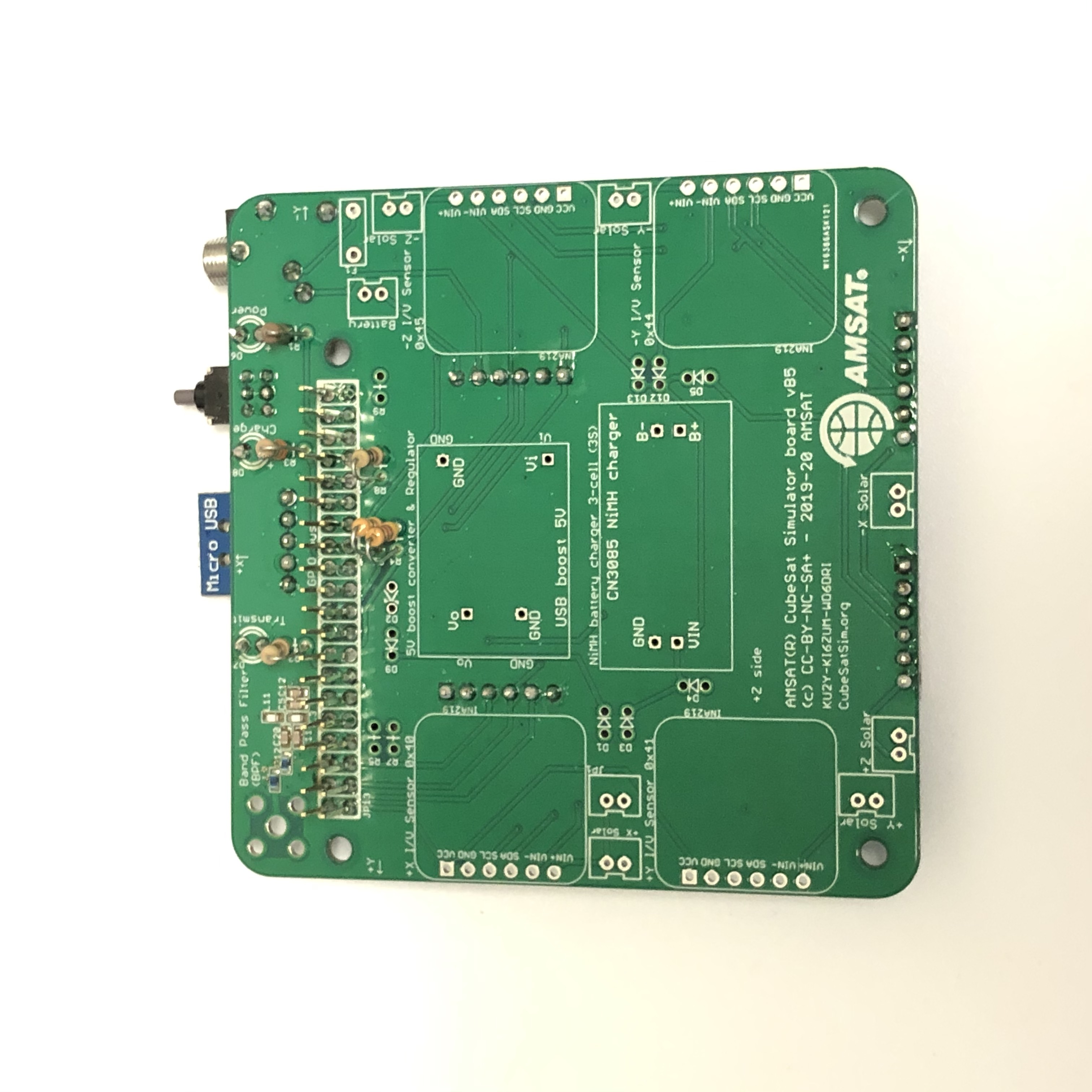
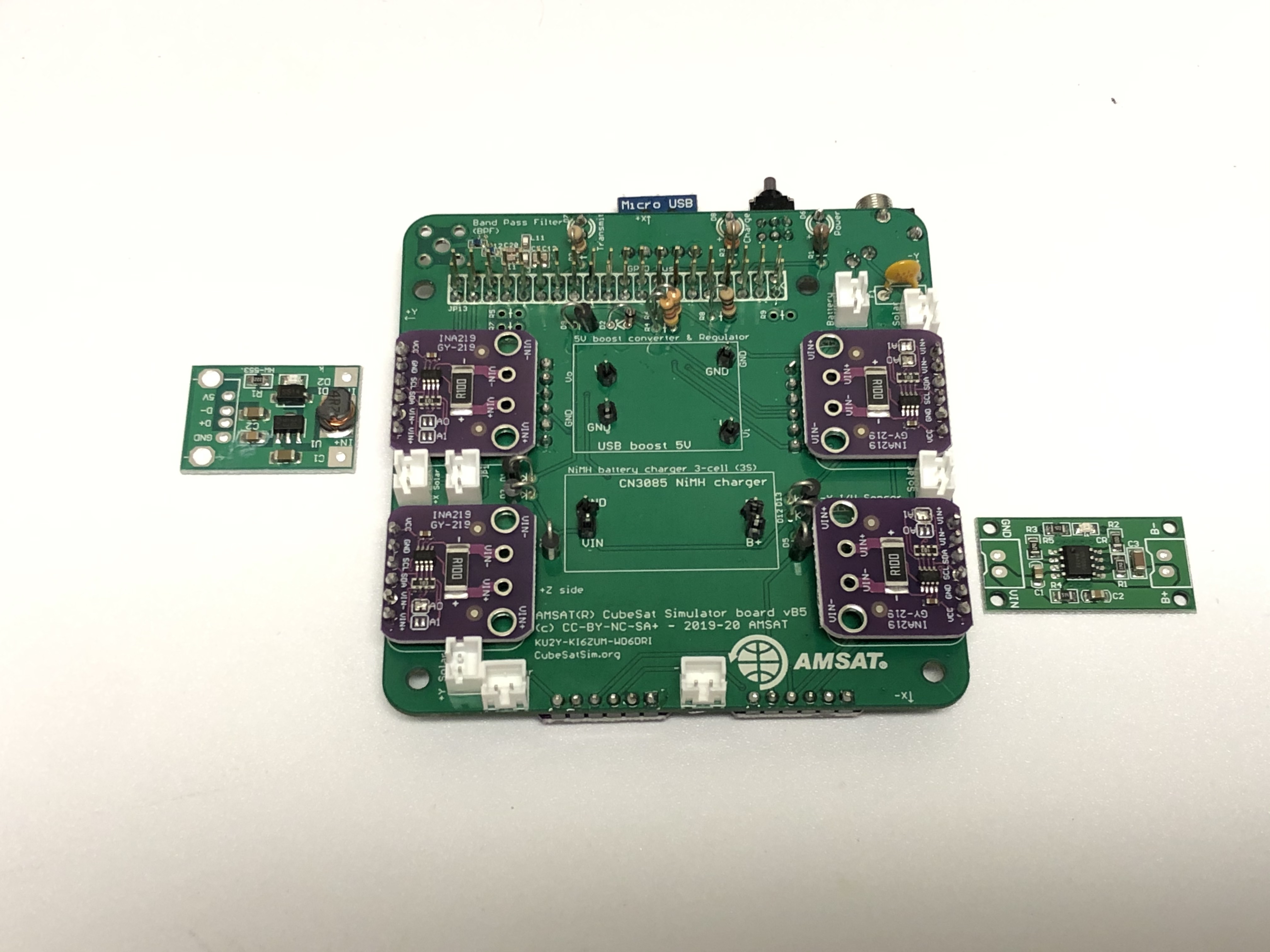
The PCB has components on both sides. This is the top of the PCB, with the AMSAT logo.
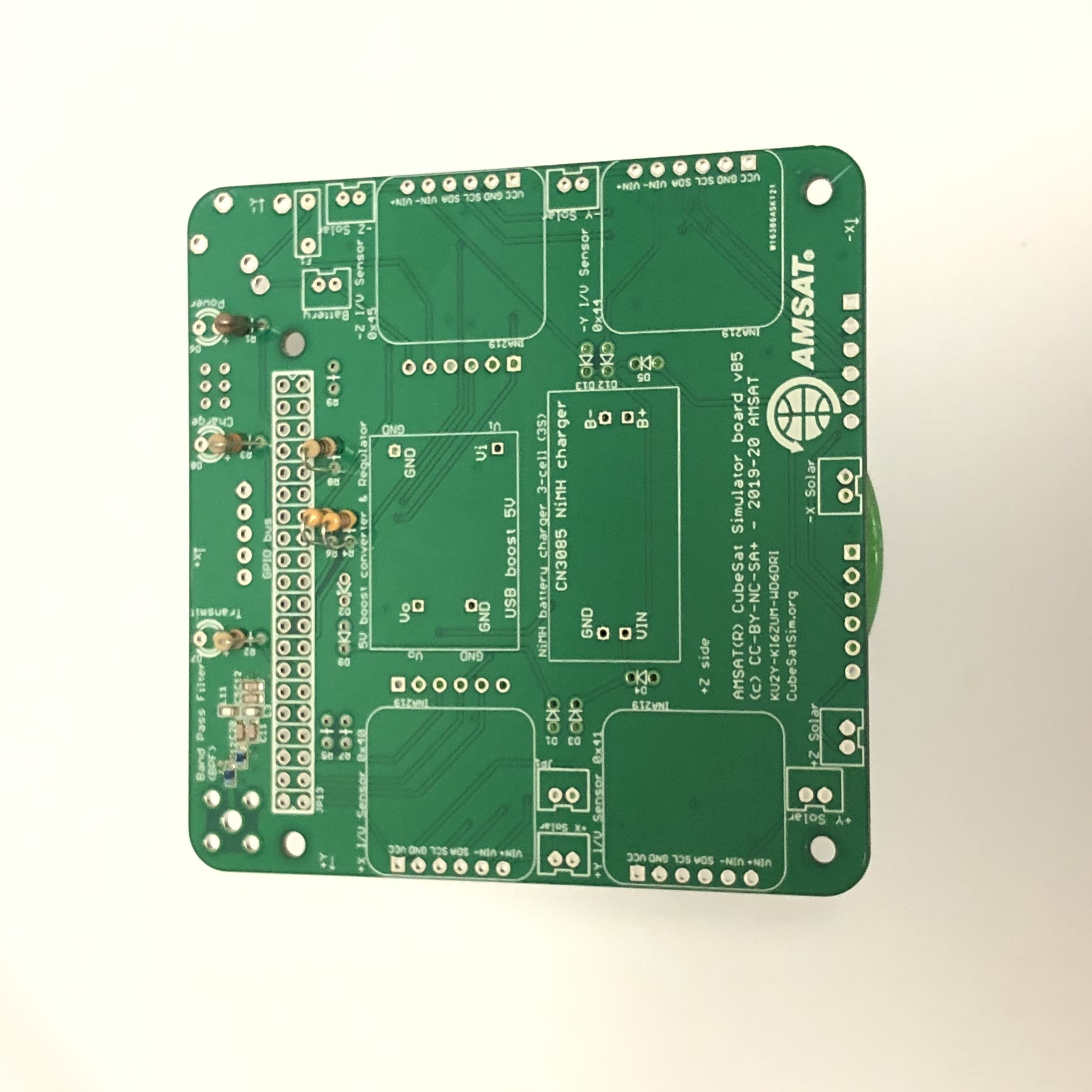
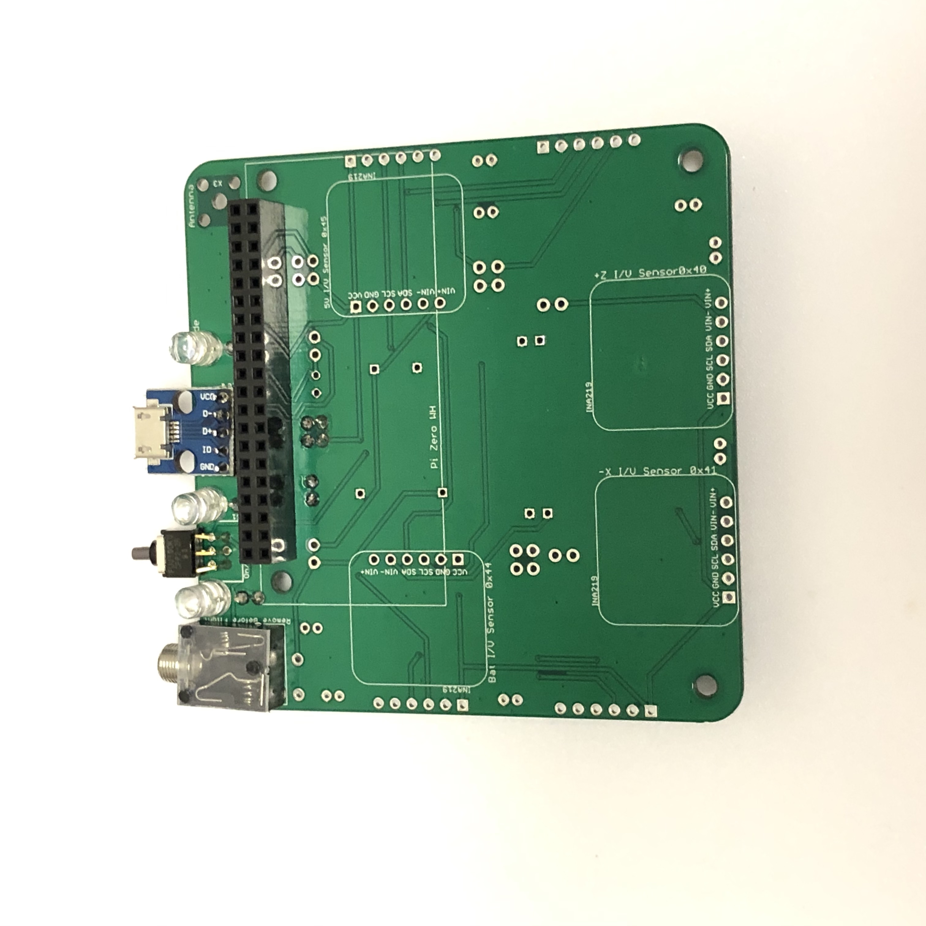
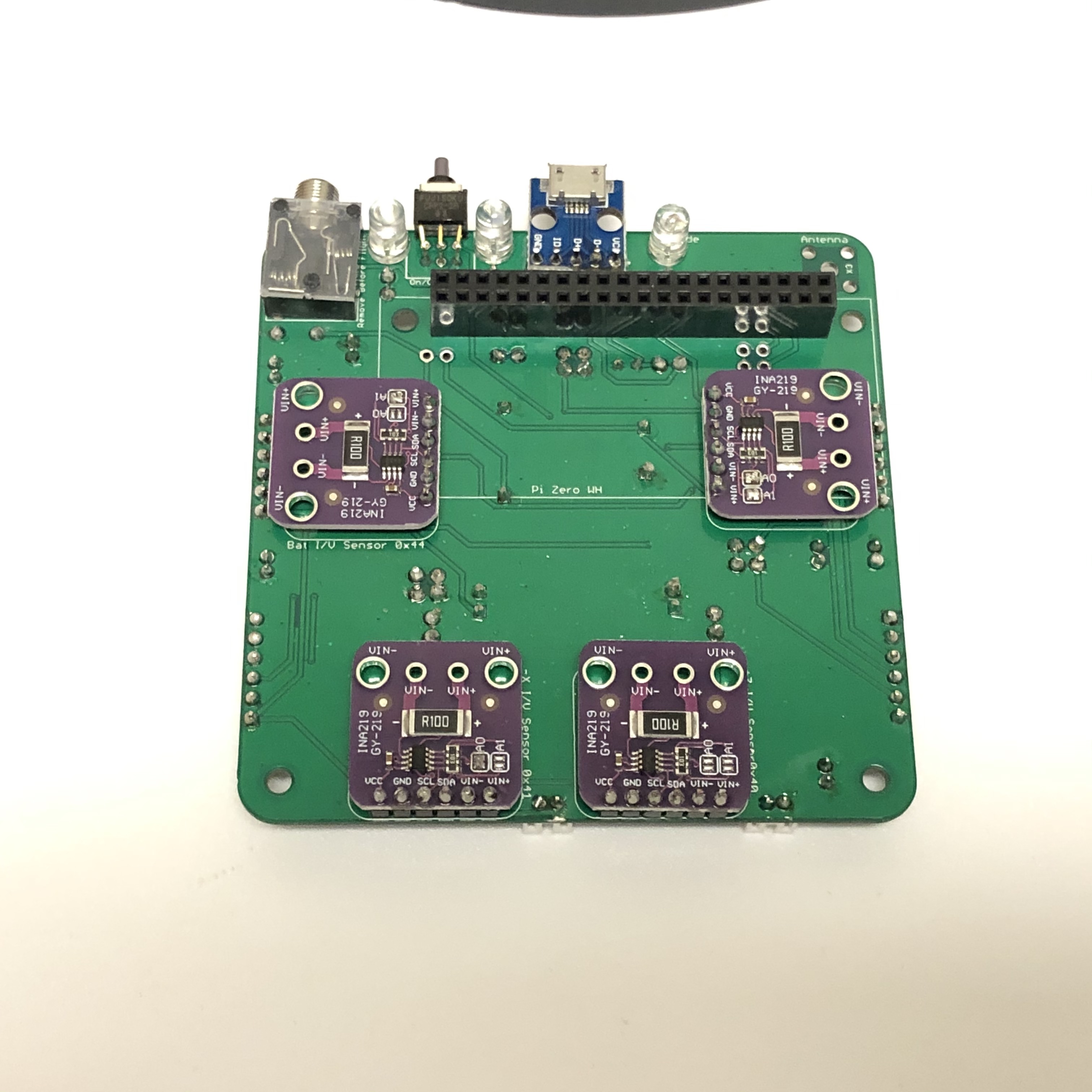
This is the bottom of the PCB.
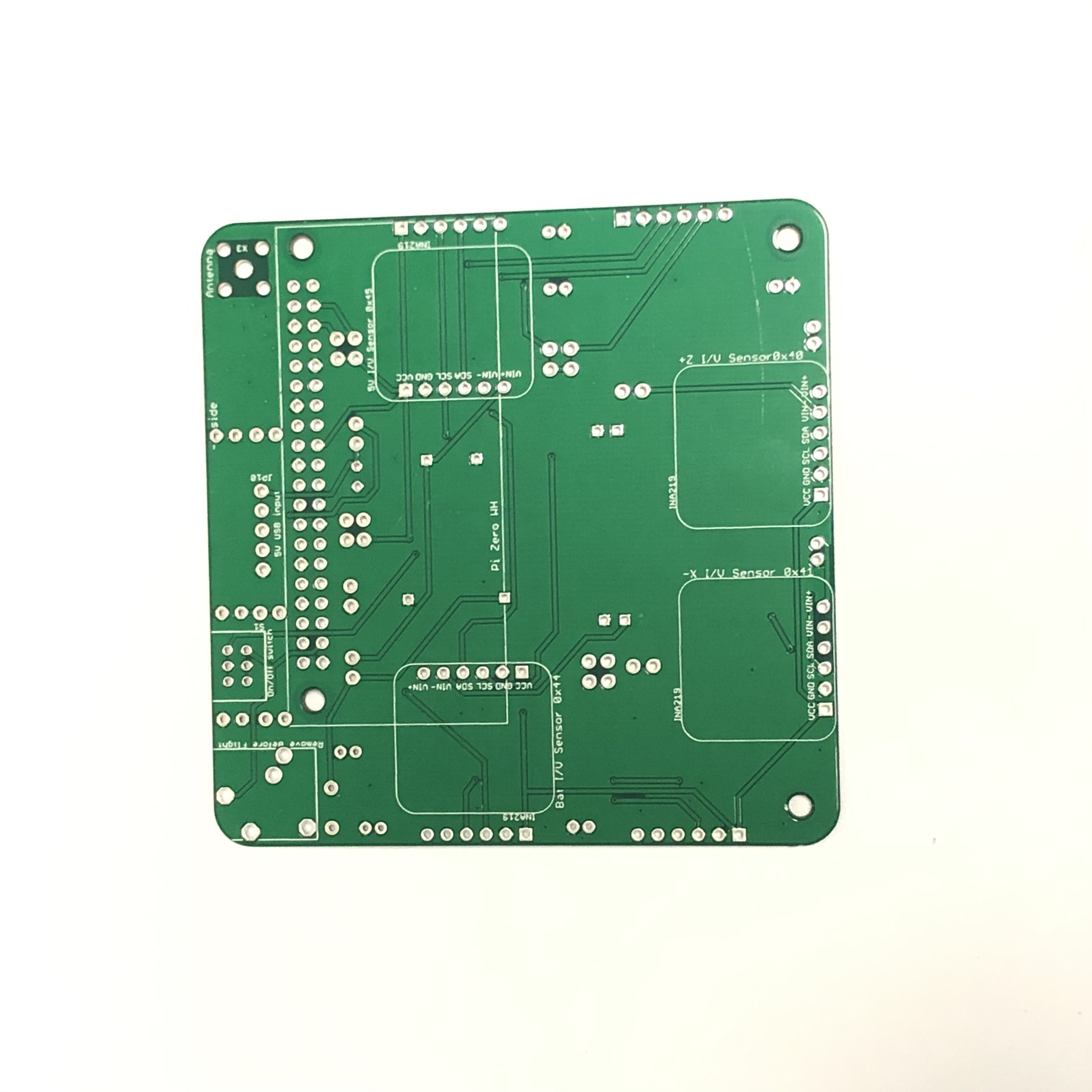
The silkscreen markings indicating which side to mount the parts. The exception is the three LEDs which are marked on the top side but should be mounted on the bottom side.
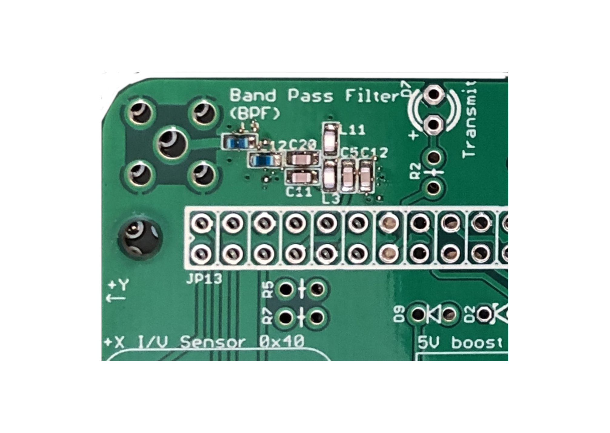
Before any components are soldered onto the board, the Surface Mount Device (SMD) components for the Band Pass Filter (BPF) must be soldered, if they aren't already soldered on. Here is a closeup of the SMD components after they have been mounted:
If you don't have the ability to do SMD soldering, you can instead use an external Band Pass Filter with SMA connectors. You will need to use a wire to bypass the SMD components:
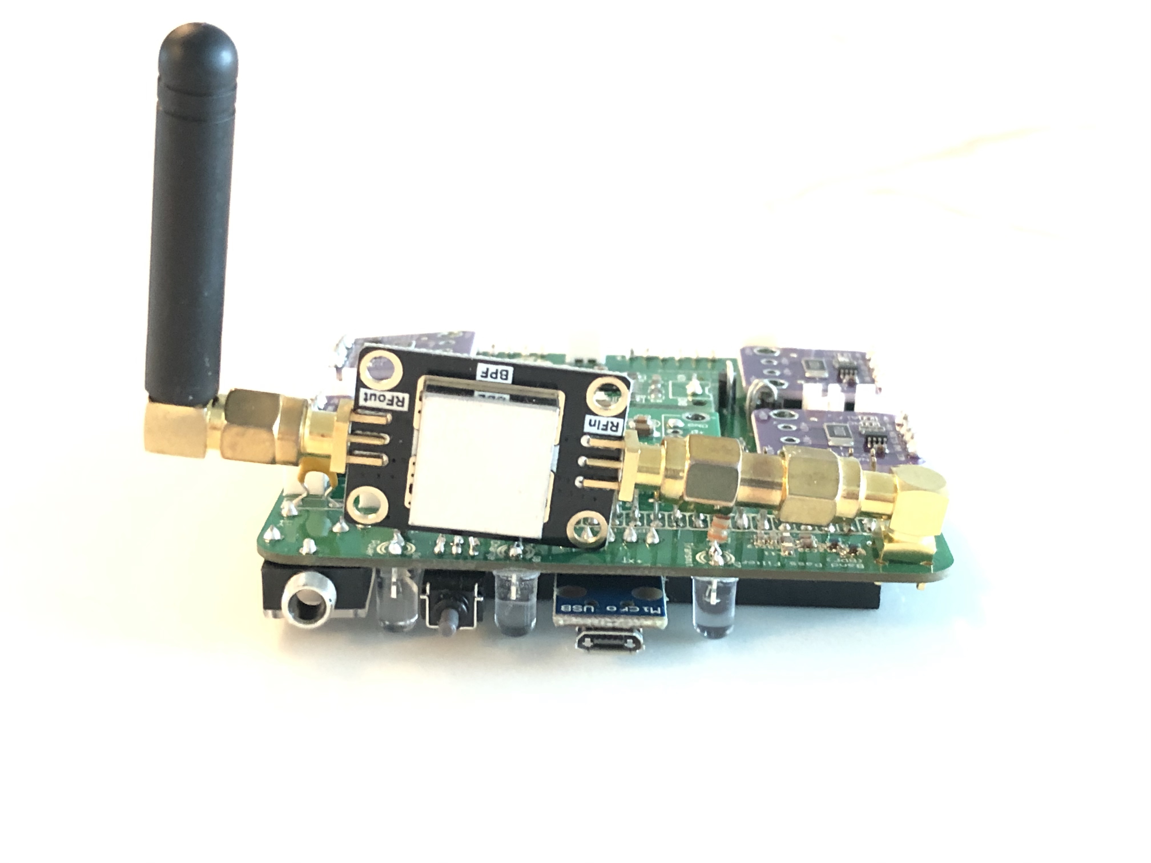
The instructions for the tape measure monopole or dipole are in the Board-Stack instructions.
Here's the board with the SMD components soldered in:
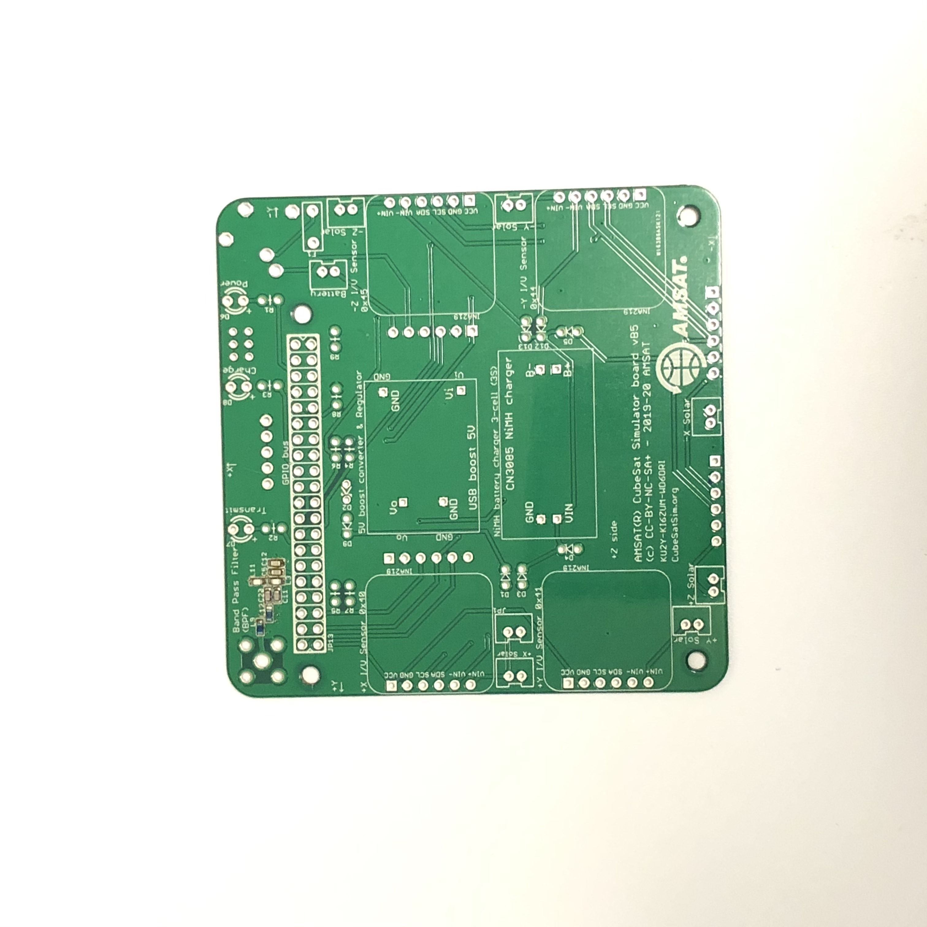
The first step is the solder the resistors R1 - R4, R6, and R8 onto the top of the PCB, as shown here.
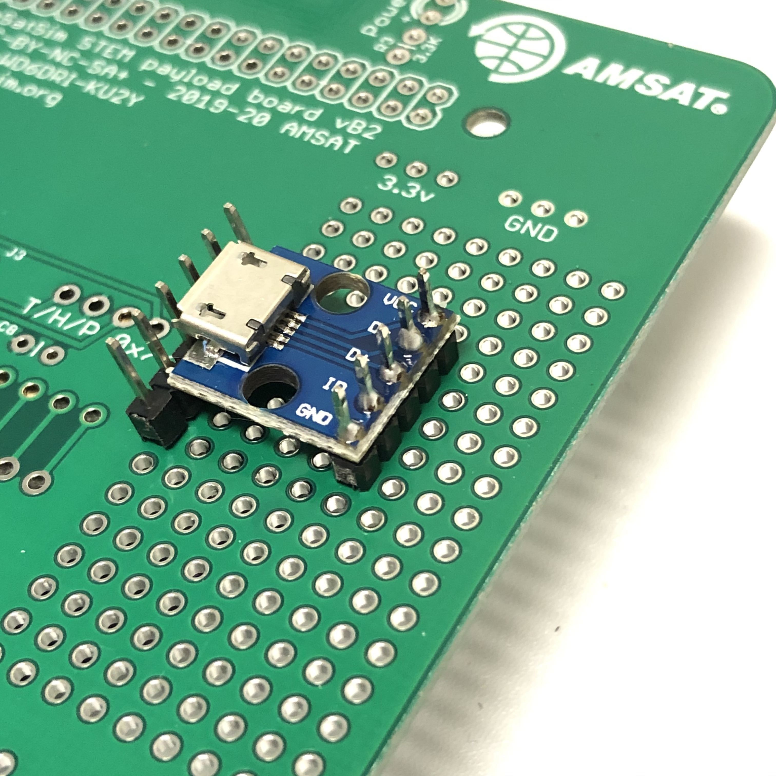
Note that R5, R7, and R9 should be left unconnected. Next, the micro USB connector, RBF switch, pushbutton switch, and three LEDs should be soldered on the bottom of the PCB. The micro USB board is first soldered to the 1x5 pin header that came with the board. One way to easily solder this straight is to use the STEM Payload board along with a 1x6 pin header from one of the INA219 boards as shown here, allowing the 1x5 pin header to be soldered:
Next, trim the excess length of the 1x5 pin headers
Then, solder the RBF switch (3.5mm audio jack), push button switch, micro USB header, and the three LED. If you are using clear lens LEDs, be careful not to mix up the colors! The longer leg on the LED is usually the '+' and should be away from the edge of the PCB:
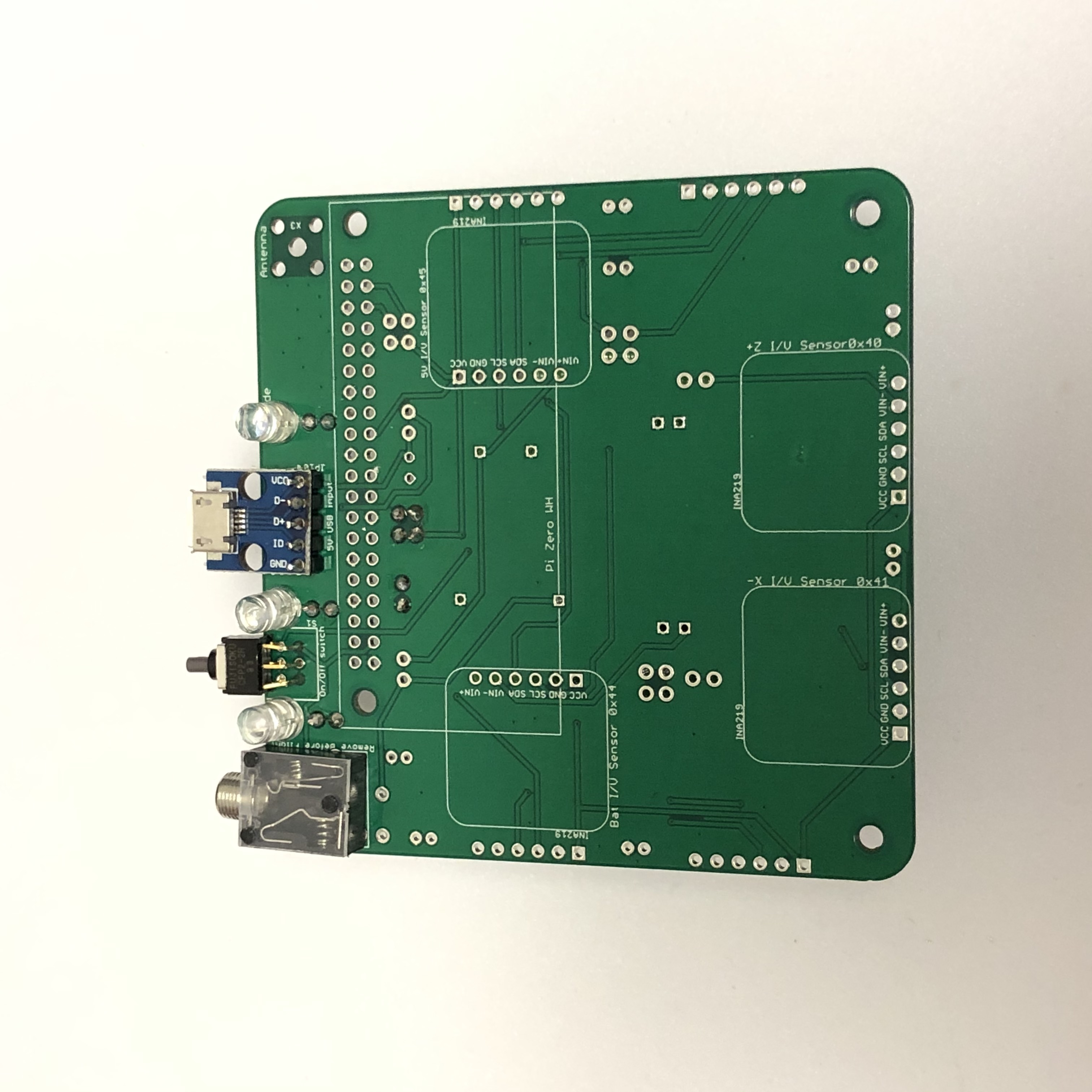
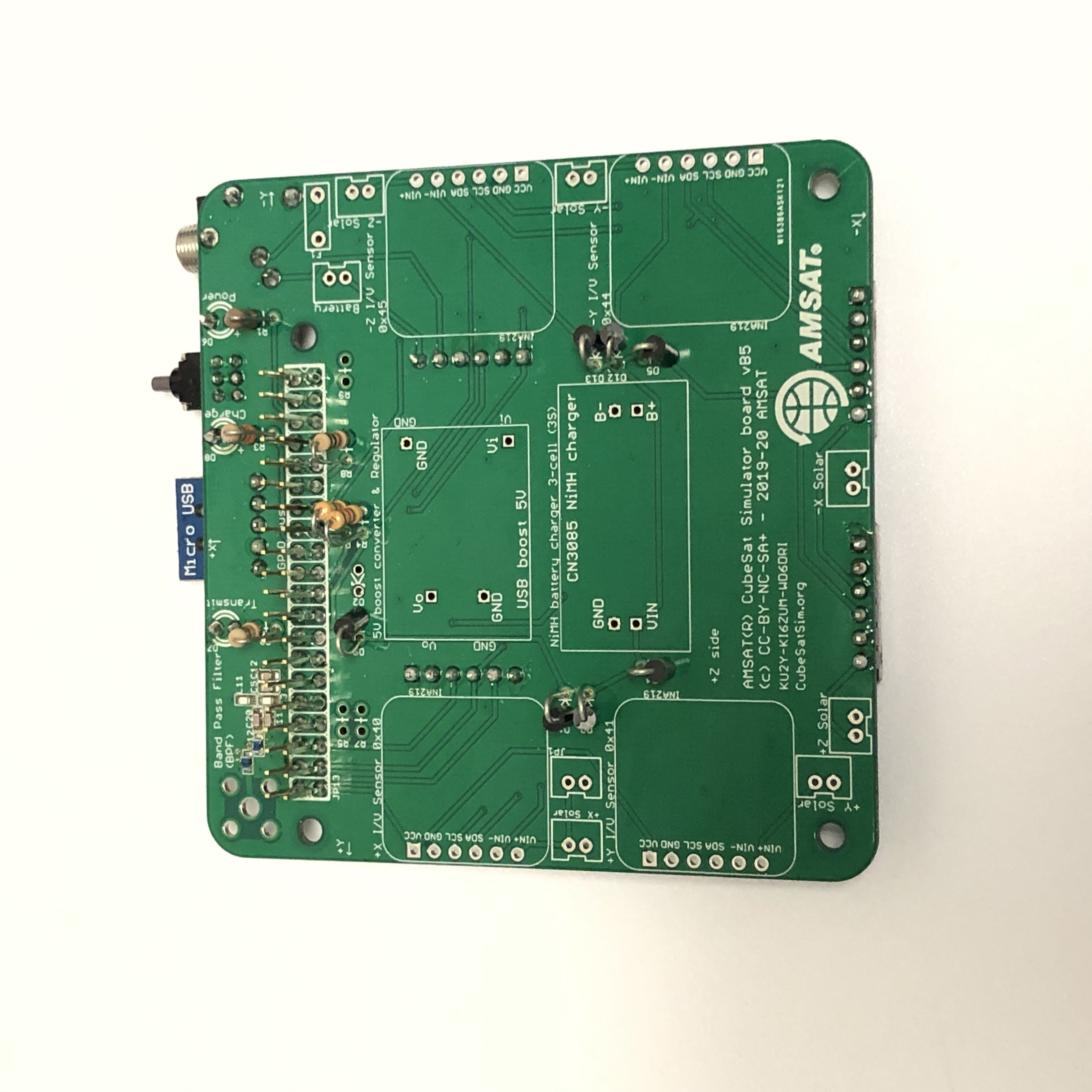
Next, solder the stacking GPIO header. The female side of the connector should be on the bottom of the PCB. The pins are soldered on the top PCB:
At this point in the build, you could do the following tests if you have completed the Software install:
Next, solder the 1x6 pin headers on four of the INA219 boards, using the same approach as for the micro USB board:
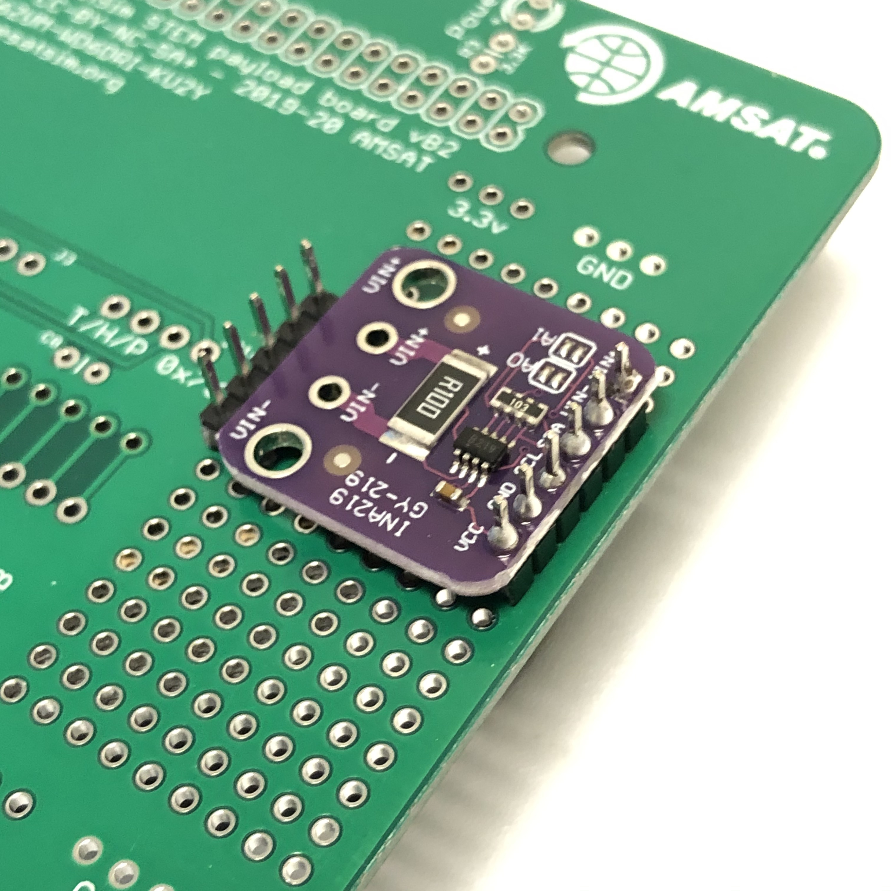
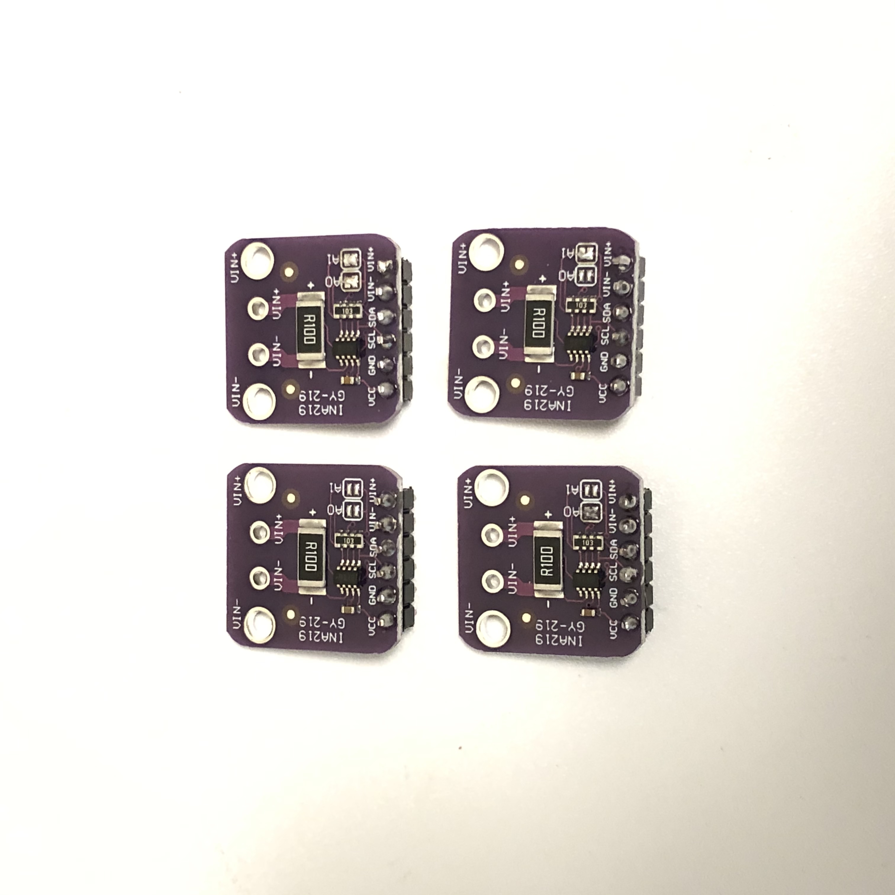
Trim the excess pin header leads. Then, set the I2C addresses to all four combinations of solder bridges on the A0 and A1 bridge pads. This will give four I2C addresses: 0x40 (no bridges), 0x41 (A0 bridge only), 0x44 (A1 bridge only), and 0x45 (A0 and A1 bridges) as shown:
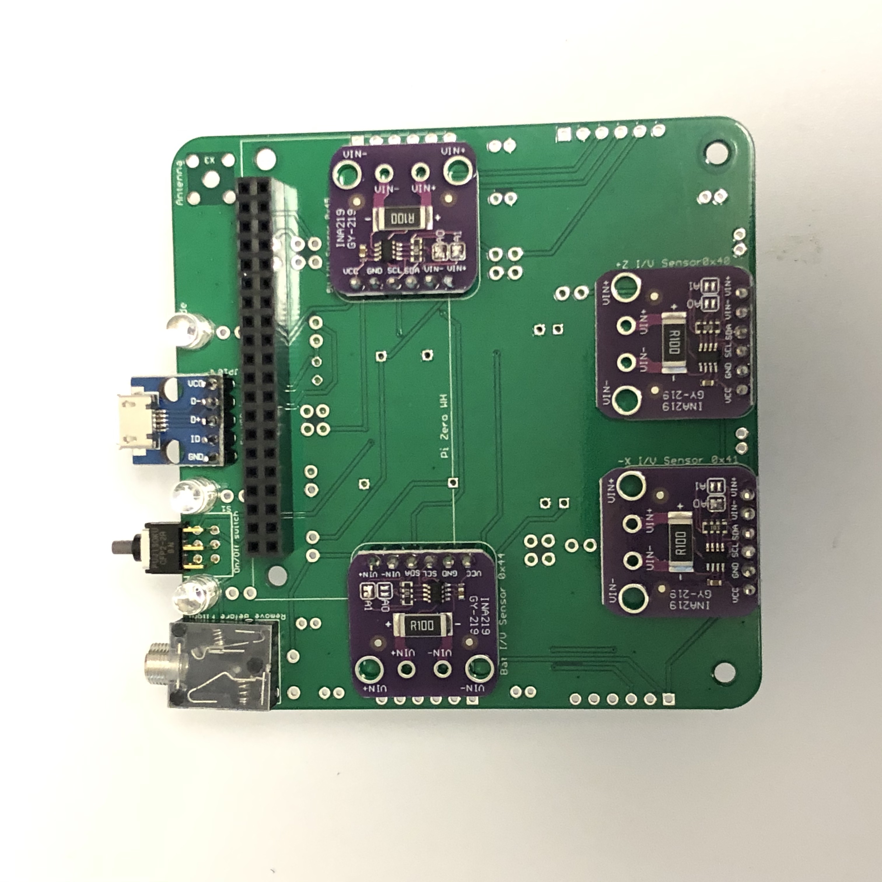
The four INA219 boards should be soldered onto the bottom of the PCB - the correct address for each one is labeled on the PCB:
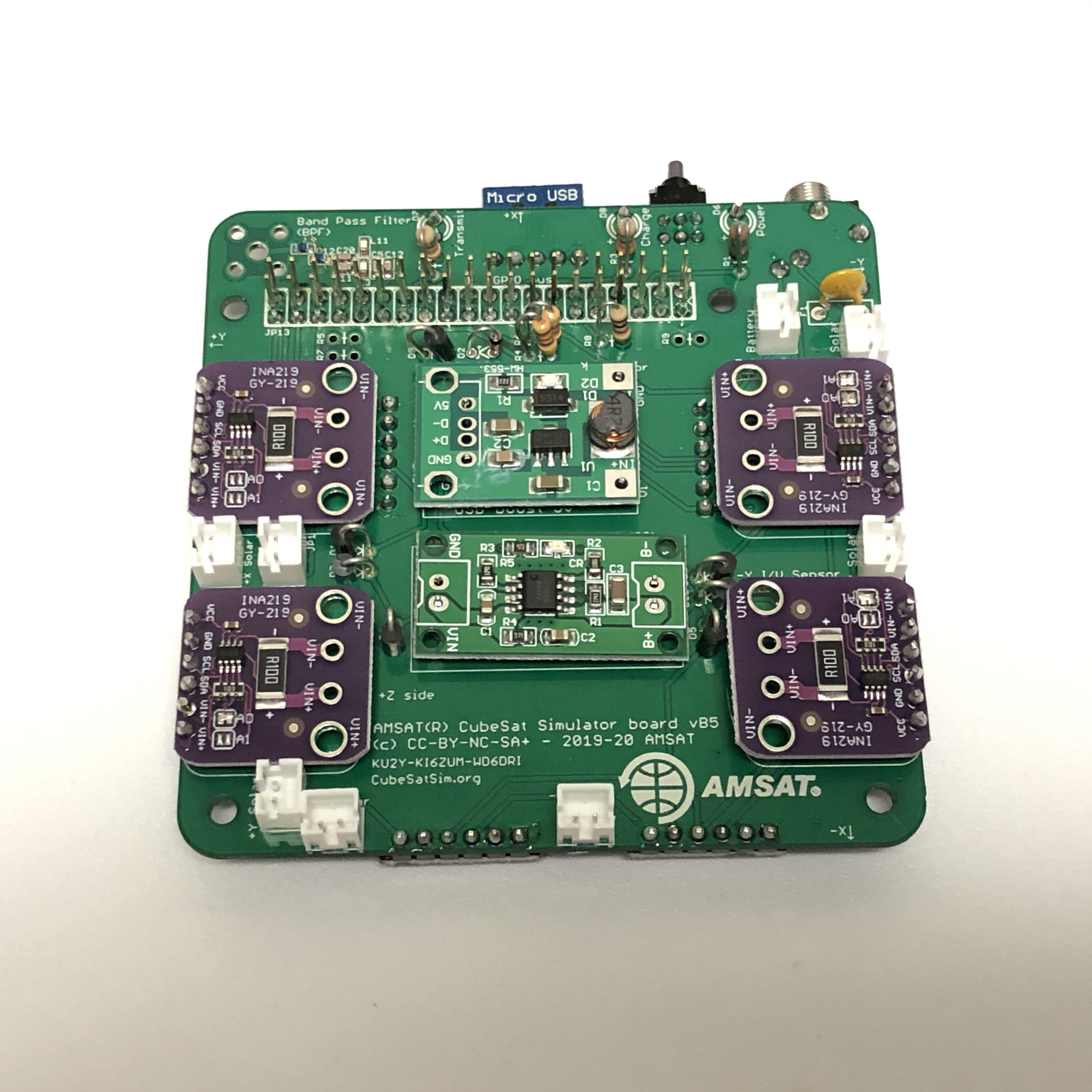
This completes the bottom of the PCB. The top of the PCB will look like this:
Next, solder the 7 1N517 diodes. Pay attention to the polarity of the diodes, and particularly the placement of D5, D12, and D13 so they do not get in the way of the -Y INA219 board. With all the diodes soldered in, the board looks like:
At this point, the following test can be performed:
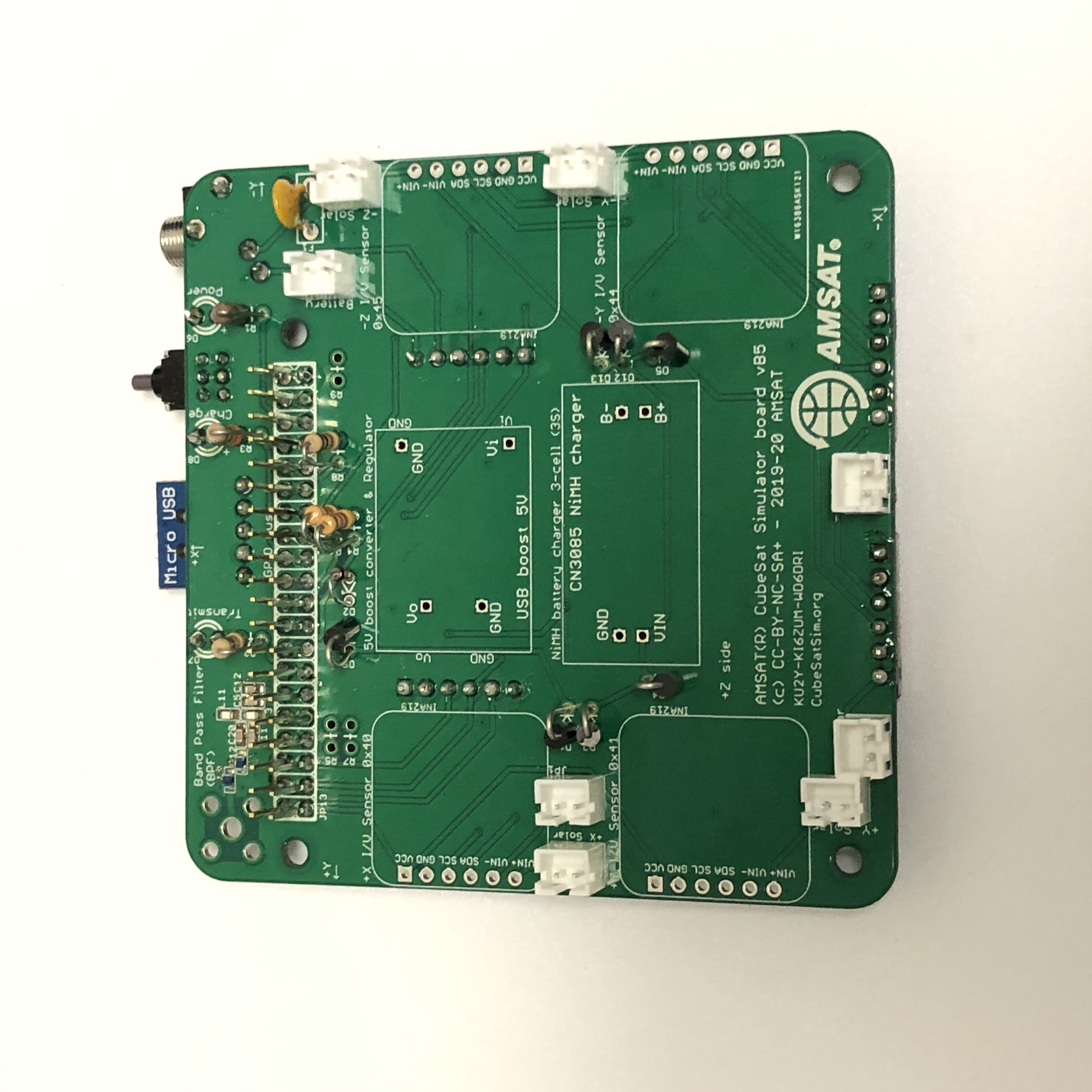
Next, solder the 8 JST 2.0 connectors, the PTC F1, and the zener diode D2, as shown:
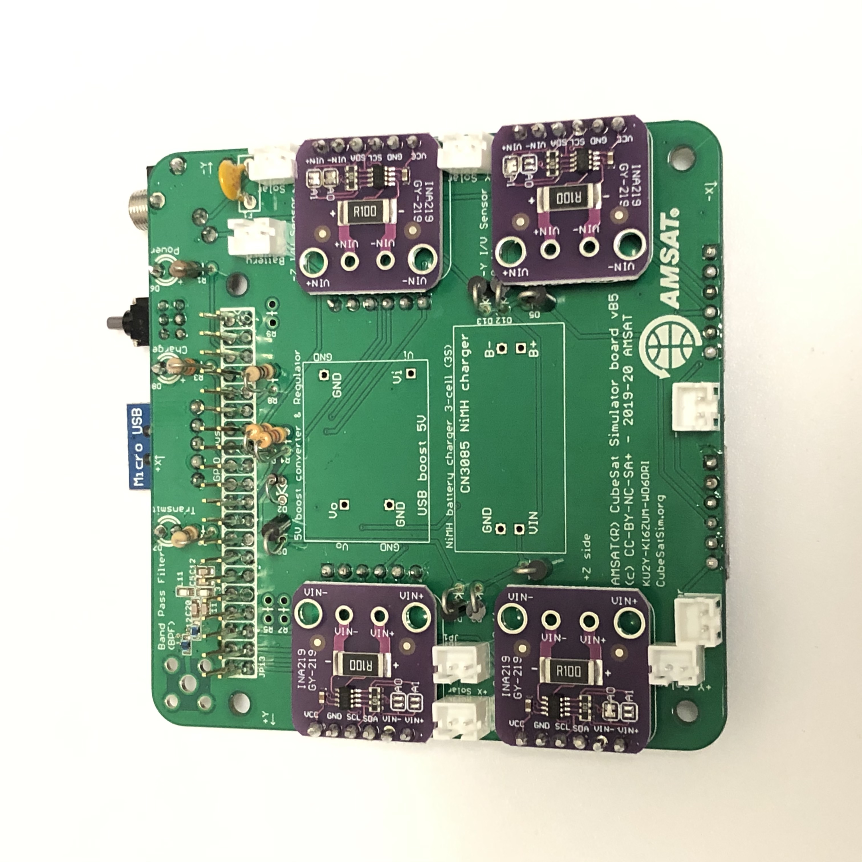
Then, prepare four more INA219s, setting the four possible addresses as before. Solder them in, paying attention to the labels on the PCB:
You are now ready to perform these tests if you have made at least one solar panel:
- Solar Panel Test
- Solar Panel Voltage Sensor Test
- Battery Voltage Sensor Test
- 5V Bus Voltage Sensor Test
Cut 8 individual pin headers, and insert in the board (do not solder yet) for the 5V boost converter board and NiMH charger board as shown:
Then, place the 5V boost converter board and NiMH charger board on the pins:
Solder the top of the pins:
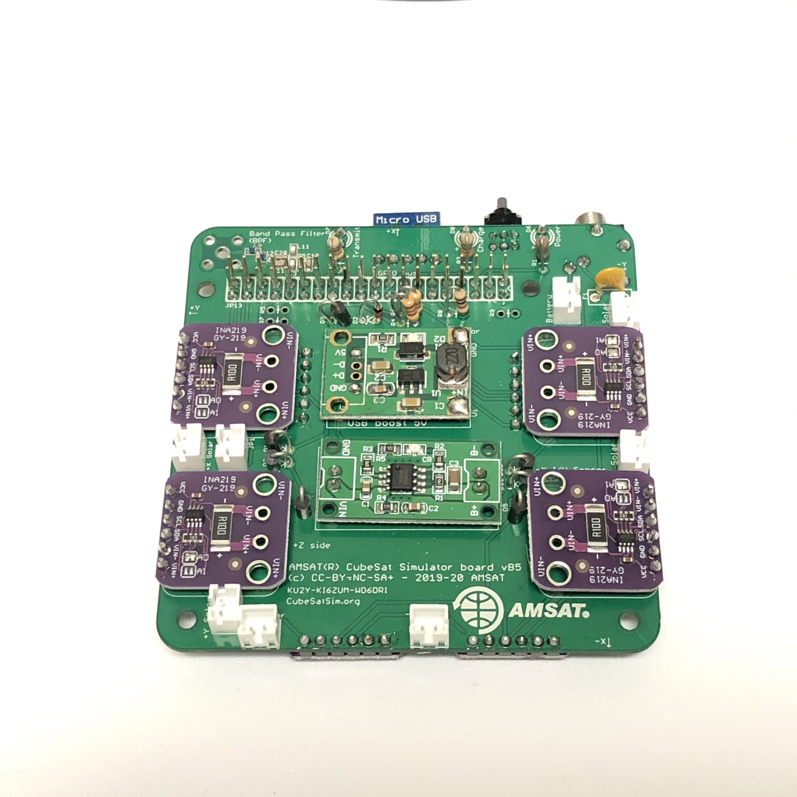
Then solder the bottom of the pins. The bottom of the PCB should look like this:
And the top should look like this:
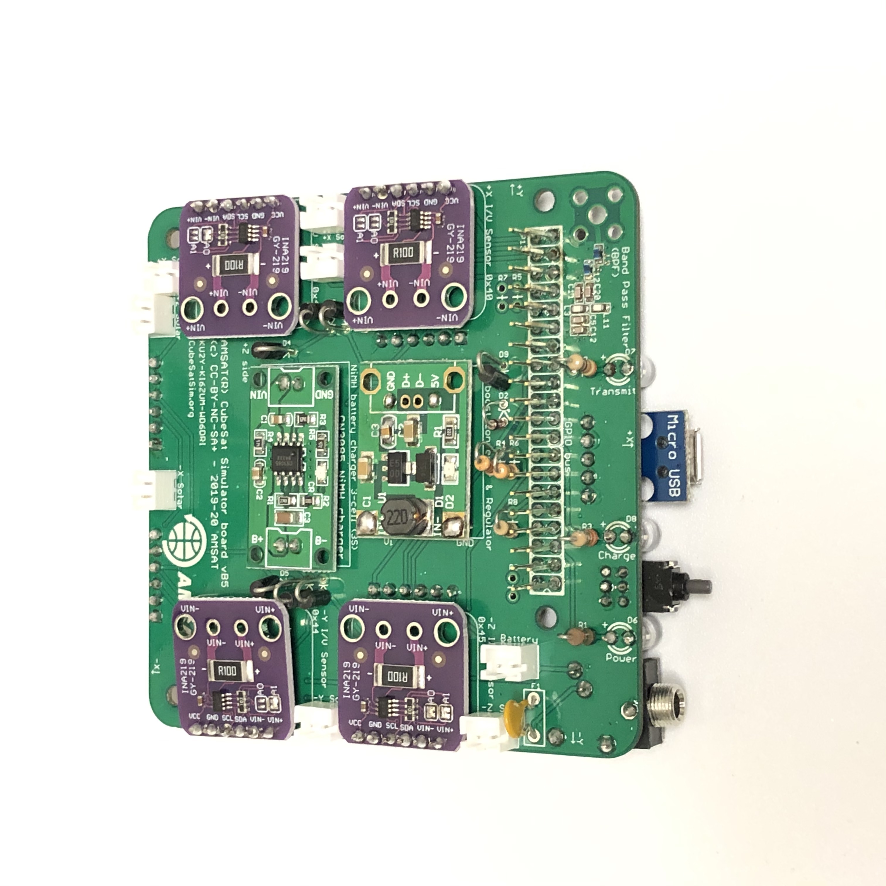
The main PCB is now complete!
You can now complete the testing with these test cases:
Battery Board Instructions
The Battery Board stacks on top of the main board. Two stacking headers are used to give sufficient spacing for the batteries.
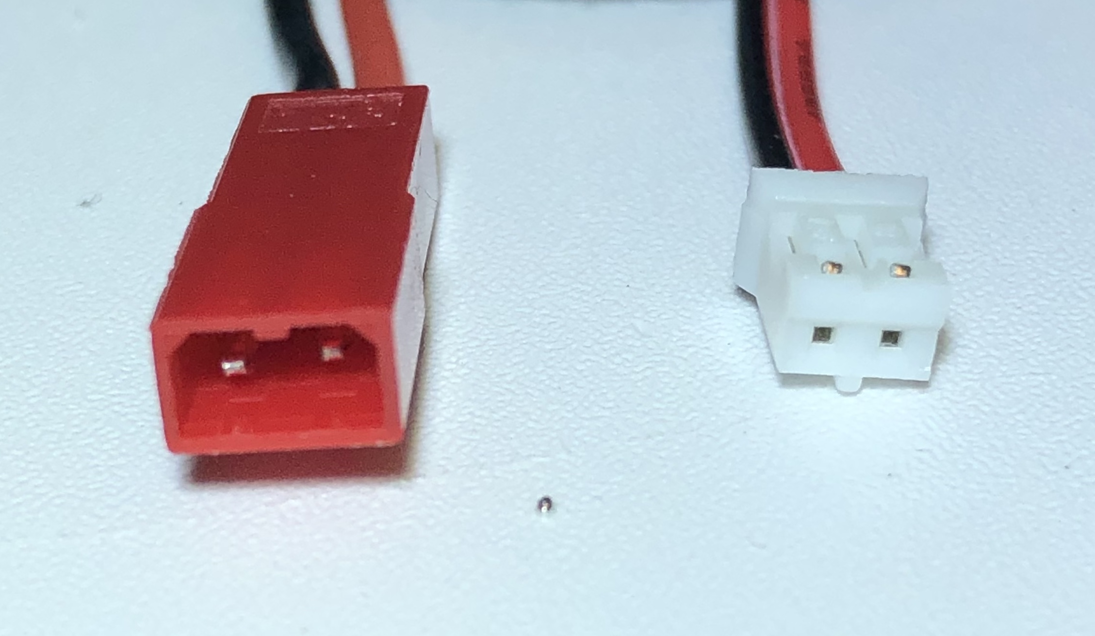
Before using any of your JST connectors, make sure they have the correct polarity. There is no standard in the industry for red and black, unfortunately, and some suppliers will supply different polarities in different orders. Verify your polarity against this image, and swap if they are reversed:
Either AAA or AA batteries can be used. I'd recommend AAA batteries for demonstrations. The CubeSatSim will discharge in about an hour, and recharge in about the same time. When doing demos, you can see changes in battery voltage over a minute or two. I would recommend AA batteries if very long demos are planned, such as continuous ones at events. The CubeSatSim will take over 3 hours to discharge and about the same time to recharge.
There is no connection on the GPIO header pins. If you just solder two pins on either side, that will anchor it in place. Soldering all 40 pins doesn't do anything useful.
Attach the 3 cell battery holder to the board and solder the red and black leads to the '+' and '-' connections. Make up a JST 2.0 cable, 4-6 inches long.
Here is a battery board with AA batteries:
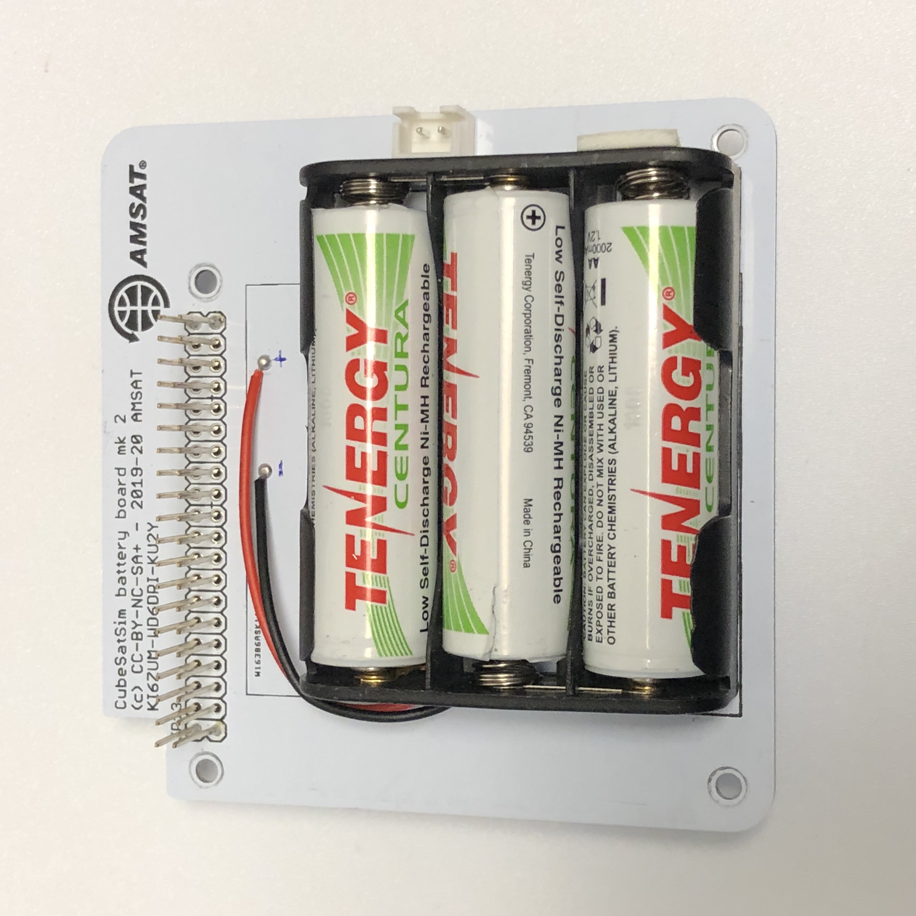
Be extremely careful of the battery polarity. There is no standard for the red/black polarity of the JST 2.0mm connectors. Some suppliers will ship different polarities at different times. Some 3 cell battery holders come with a JST 2.0mm connector on them. Again, double check the polarity to be sure it is correct. When testing the polarity with a digital voltmeter, be very careful not to short the pins together, as this could damage the battery or cause a hot spot.
Next, build the STEM Payload Board.
Now you are ready to put the Board Stack together.