4. Main Board 2 - alanbjohnston/CubeSatSim GitHub Wiki
If the images in this page fail to load, you can download a PDF of this page here.
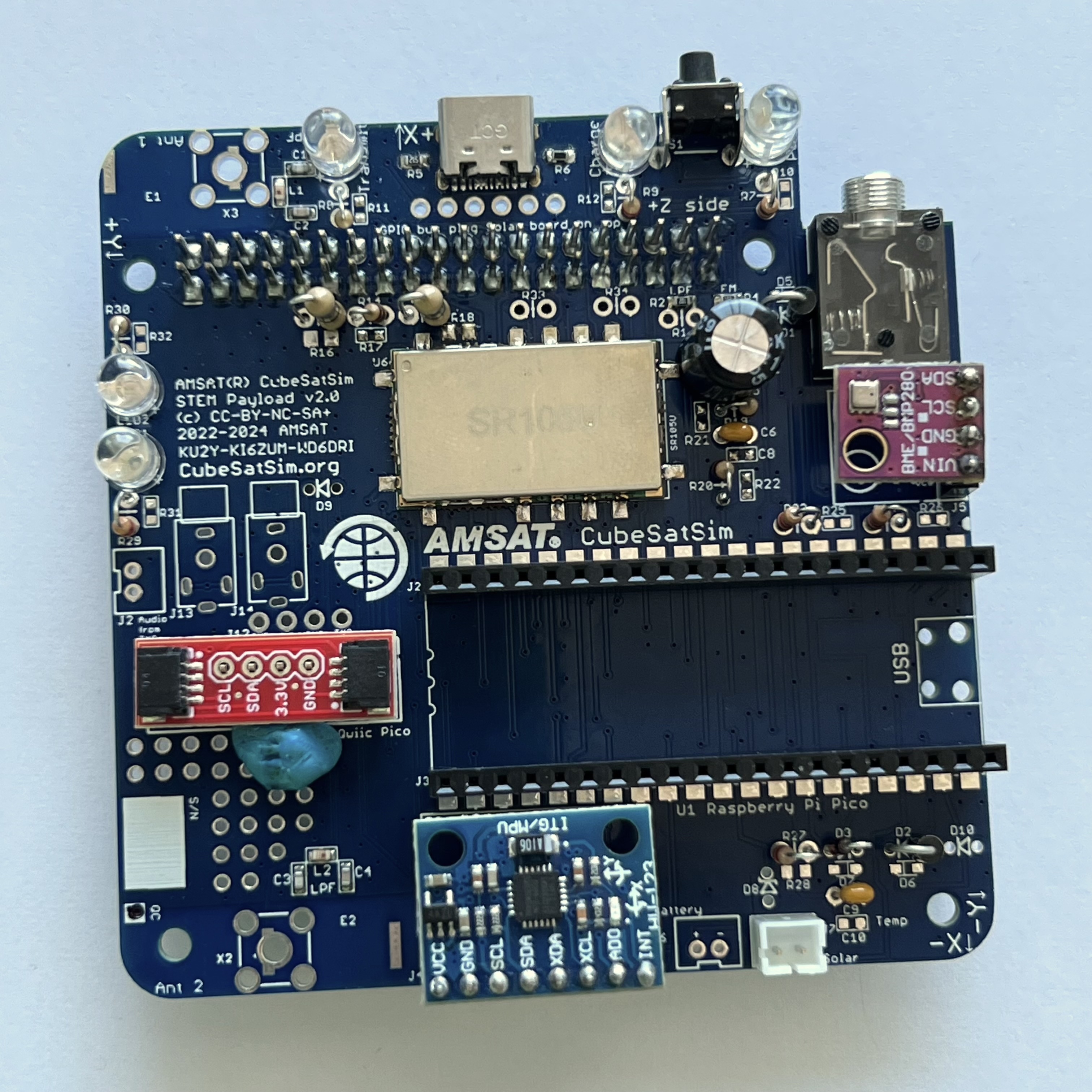
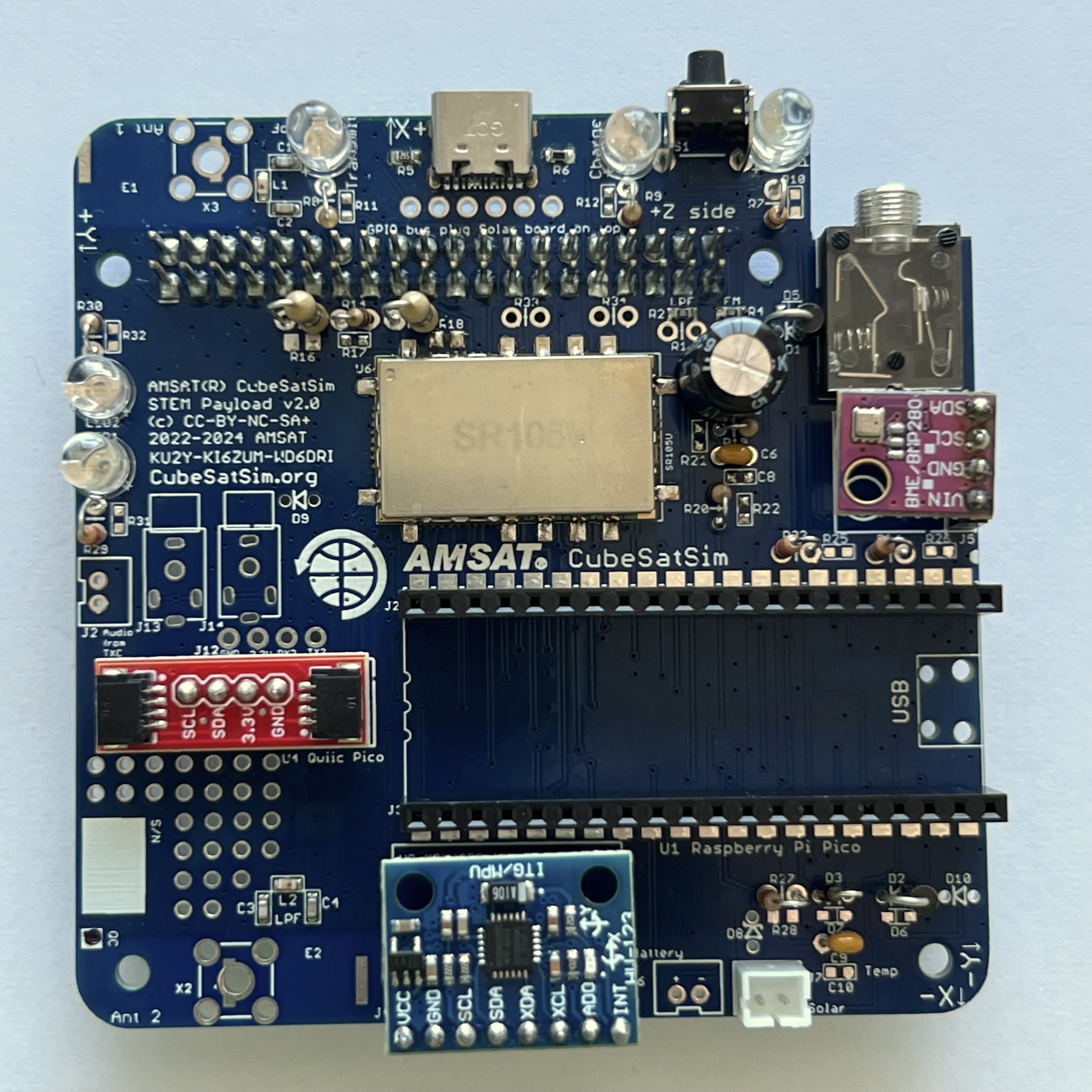
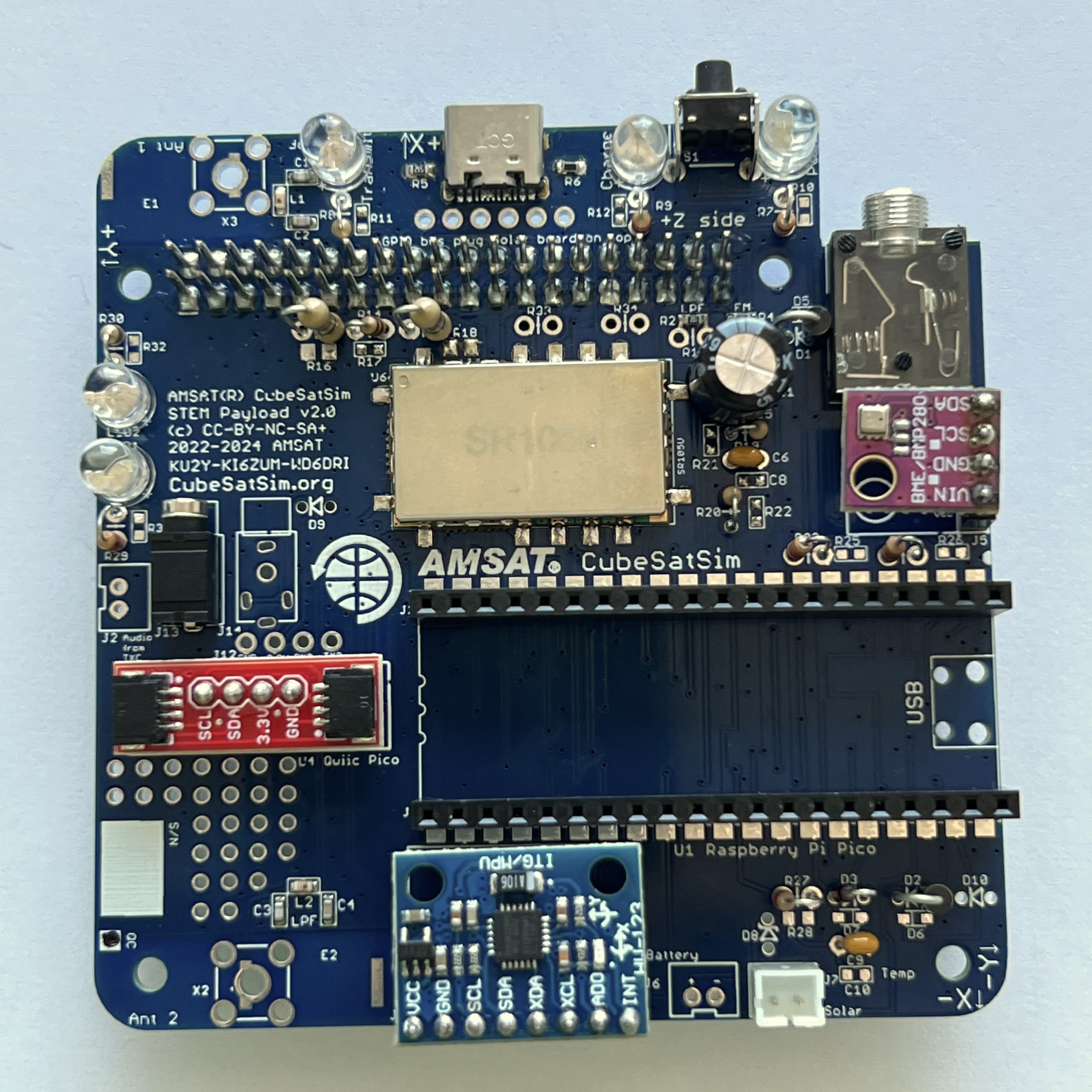
4. CubeSatSim Main Board Assembly Part 2
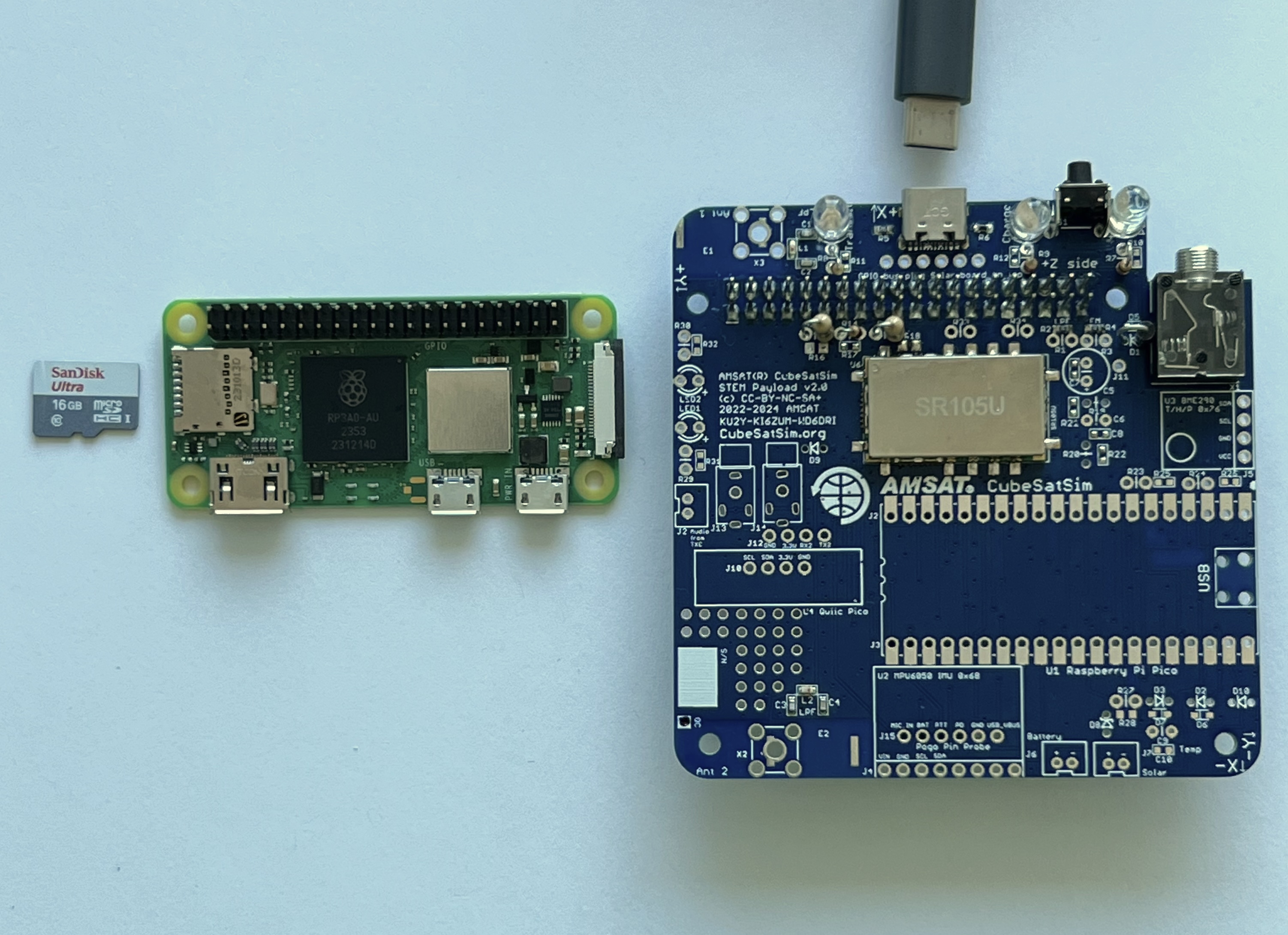
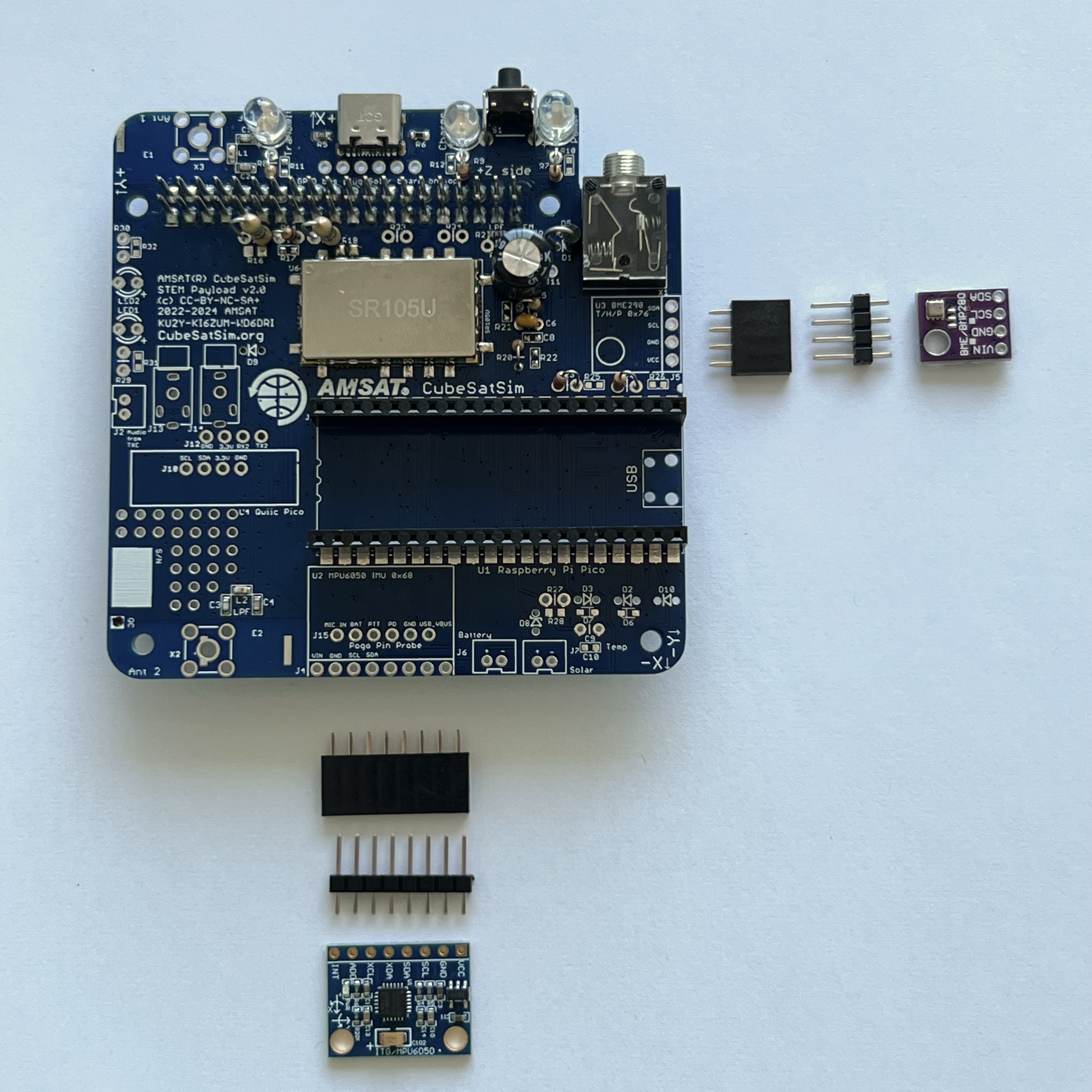
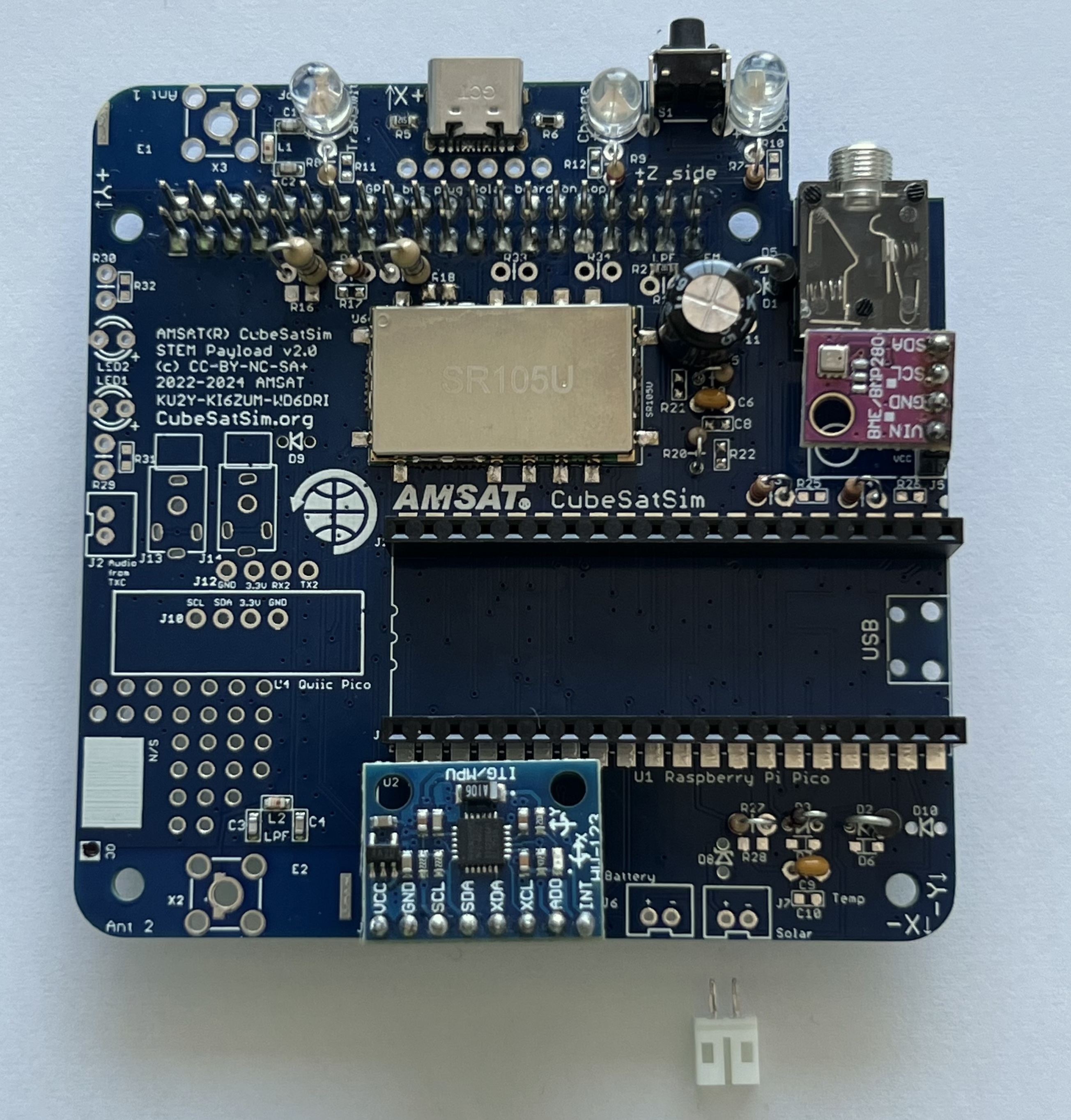
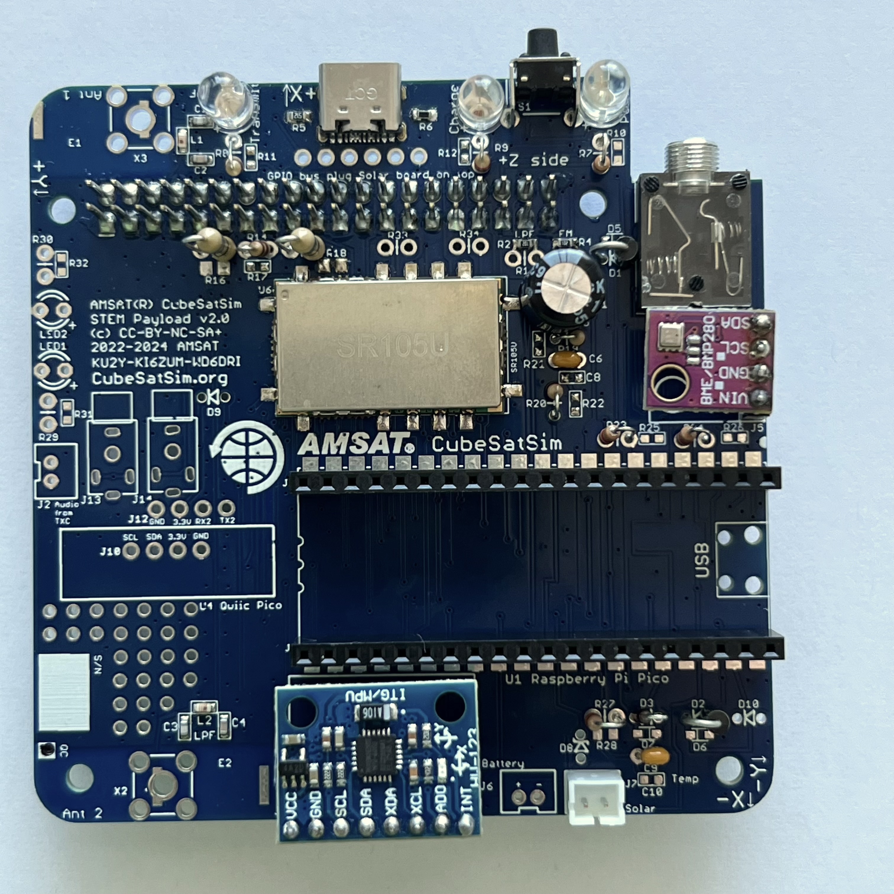
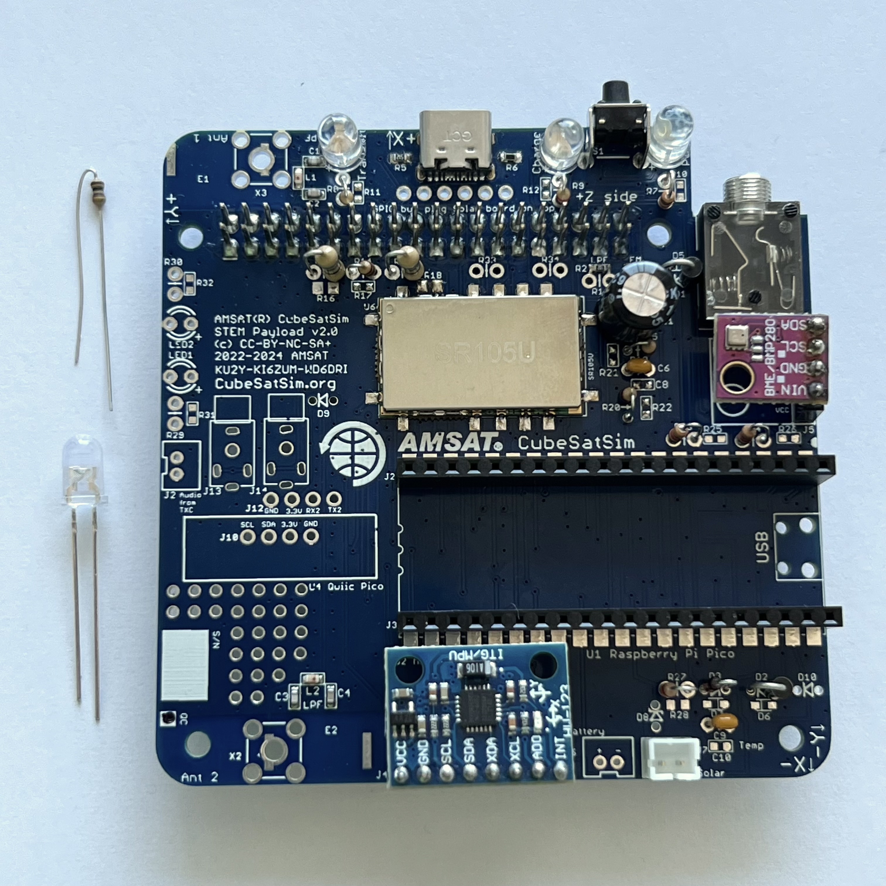
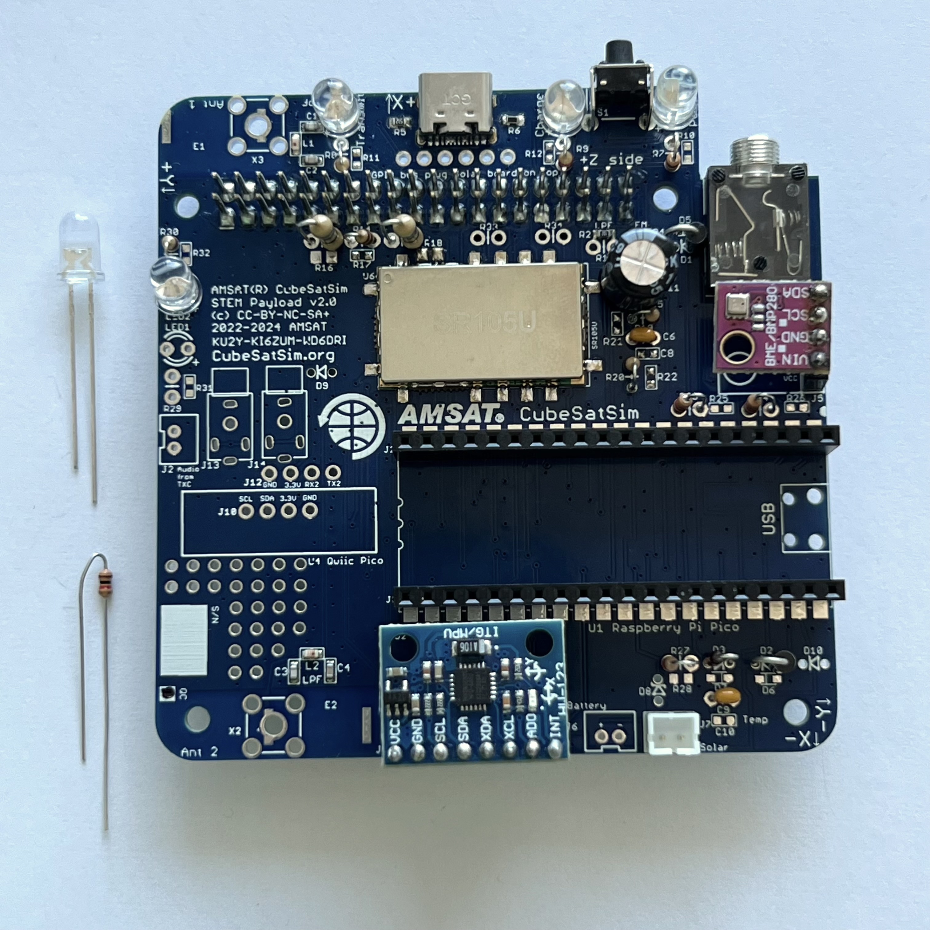
After Part 1, here is the Main board:

Note that some of the photos in this step show the v2.0 board (there is no yellow PTC), but there are no other differences between the v2.1 and the v2.0 board.
We can now start doing some intermediate tests on the board.
You will need these tools:
- Safety glasses (to protect eyes while soldering or trimming leads)
- Soldering iron and solder (I use lead-free solder, but leaded solder is easier to work with)
- Needle nose pliers (to bend leads and hold parts)
- Side cutters (to trim leads)
- glue, such as super glue to attach the JST connectors to the PCB
Other tools that are helpful:
- Blue mounting putty(to hold components in place while soldering)
The first part of this step is testing while the second part continues the assembly
Checklist
Here is the Bill of Materials: https://CubeSatSim.org/bom
The BOM has a sheet "By Steps" which lists the parts needed for each step in order. If you have a Google account, you can make a copy of this spreadsheet ("File" then "Make a Copy") and check off each part as you install it.
For example, here is the checklist for this step:
Schematic
Here's the schematic for the v2.1 Main board for reference:
4.1 Testing
Video
Here is a video of the testing part of this step.
Pi Blink Test
For these tests, you will need your Raspberry Pi Zero 2 or Pi Zero, a micro SD card with the CubeSatSim software installed (see the Software Install instructions), and the USB-C power cable (or a micro USB power cable or adapter if you power it directly to the Pi).
If your Pi Zero 2 does not have the 2x20 pin header installed, you will need to carefully solder it in. The pins should stick up on the side that has the ICs and the SD card holder.
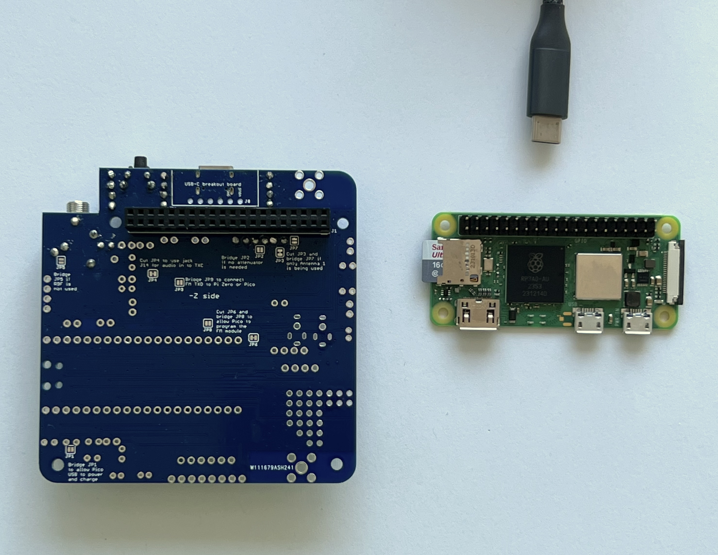
Flip the Main Board upside down and plug the Pi Zero 2 into the bottom of the board so that it looks like this:
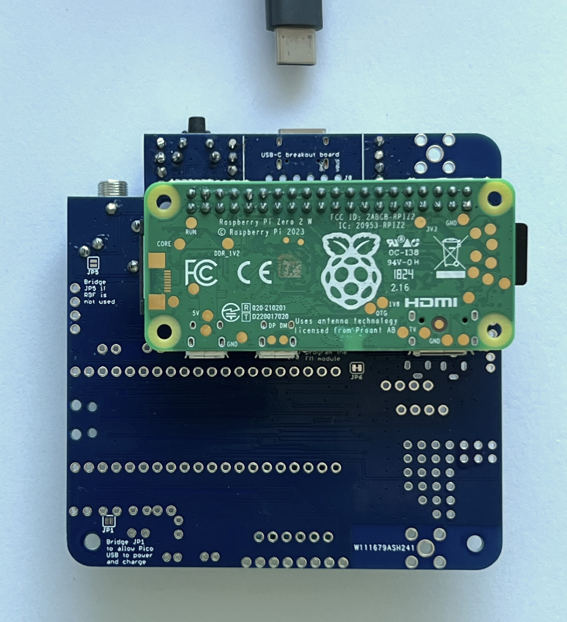
Plug your USB-C power cable directly via the PCB USB-C port. The Pi will turn on and the tiny green LED on the Pi will be on or blinking. Note that the LED is on the top of the Pi Zero 2 board, but you can see it through the lower left mounting hole, or from the side:
If you don't see this, make sure you have your micro SD card with the CubeSatSim software installed and the USB cable providing power to the Pi.
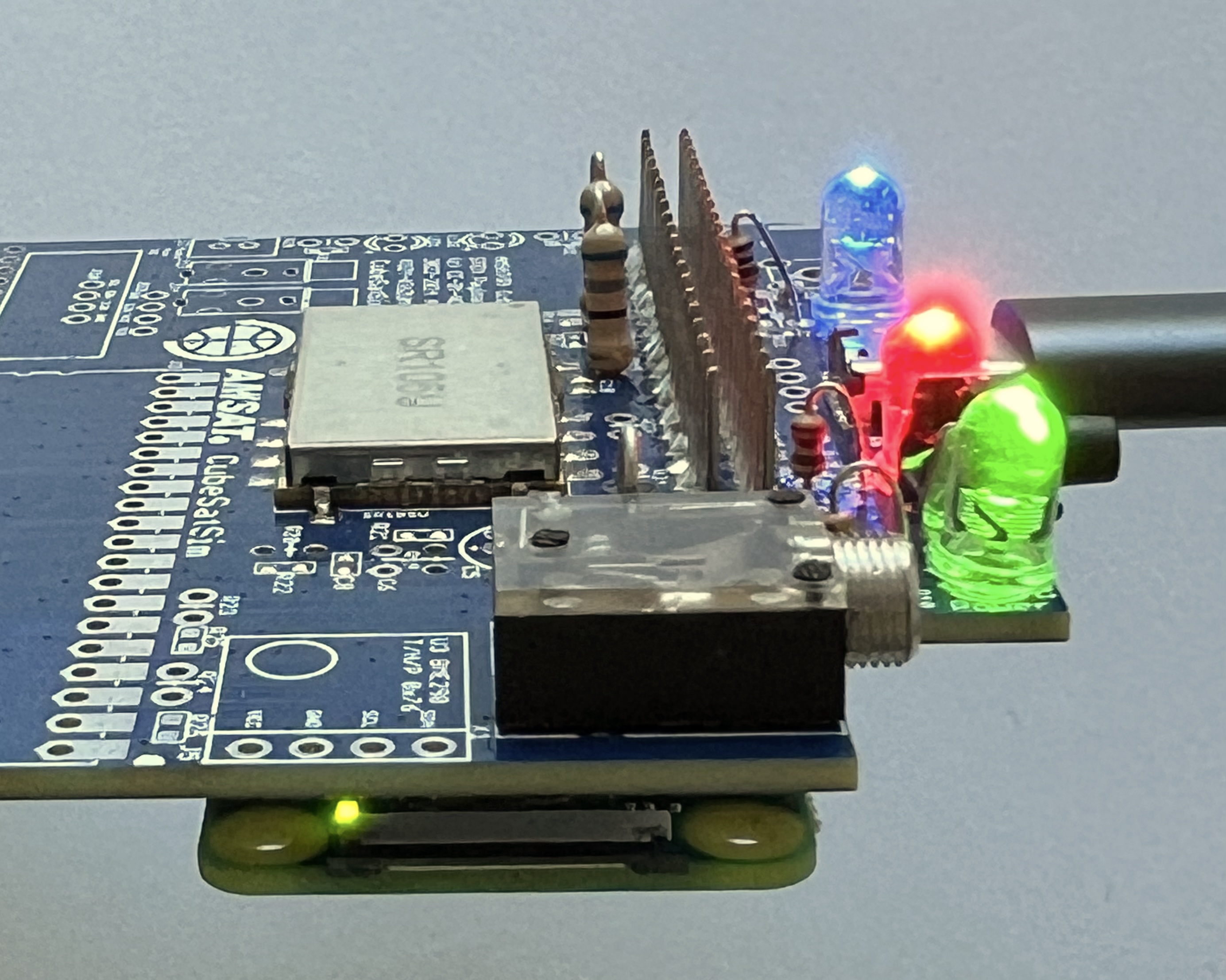
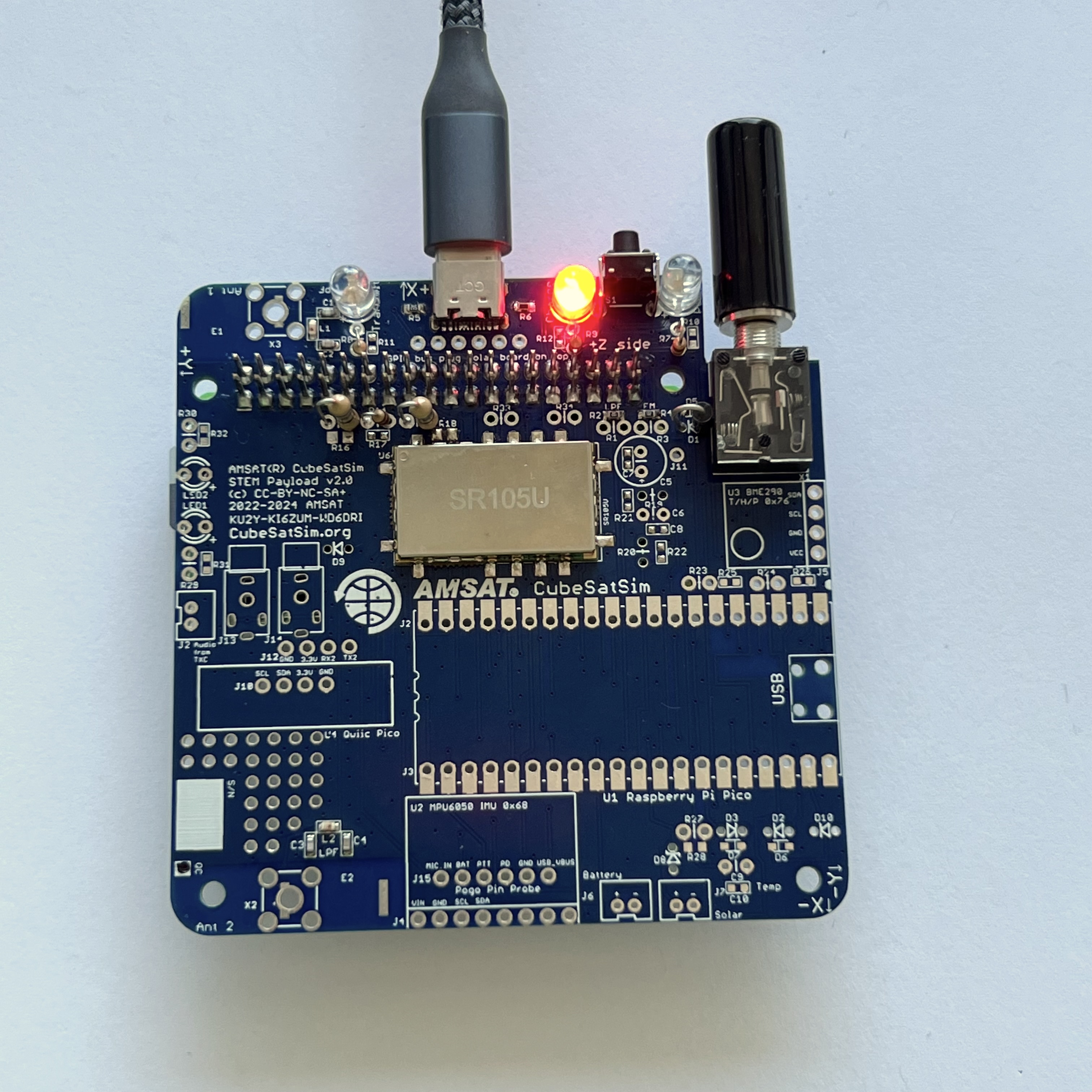
With the USB-C cable plugged into the board, the Red LED will be illuminated:
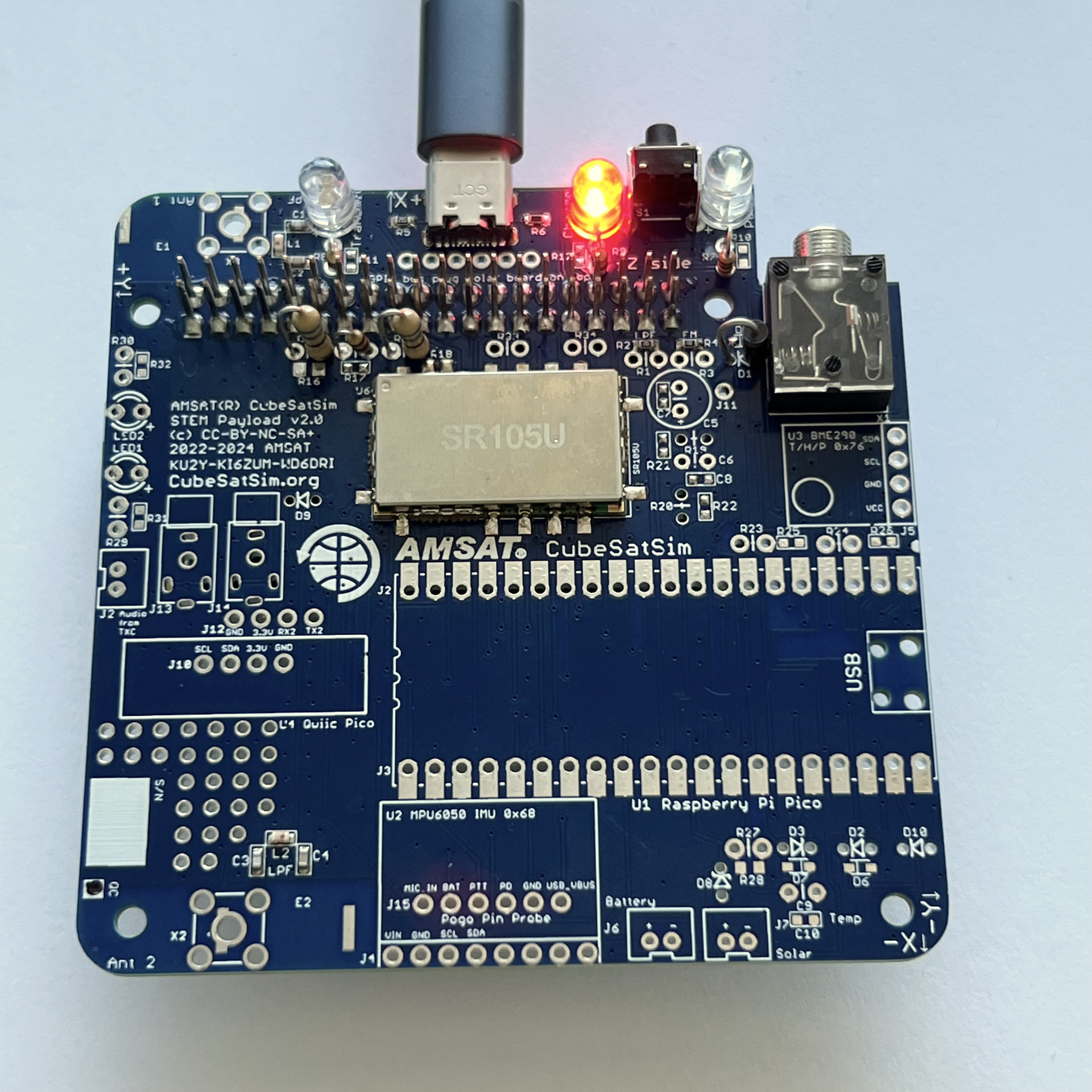
If the LED doesn't illuminate, it might mean there is a problem with the red LED LED5 or resistor R9 or the USB-C connector J9 or resistors R5 or R6.
Power LED Test
With the Pi plugged into the main board and the power cable plugged into the Pi micro USB port, about 30 seconds after booting, the CubeSatSim software will run and turn on the green Power LED.
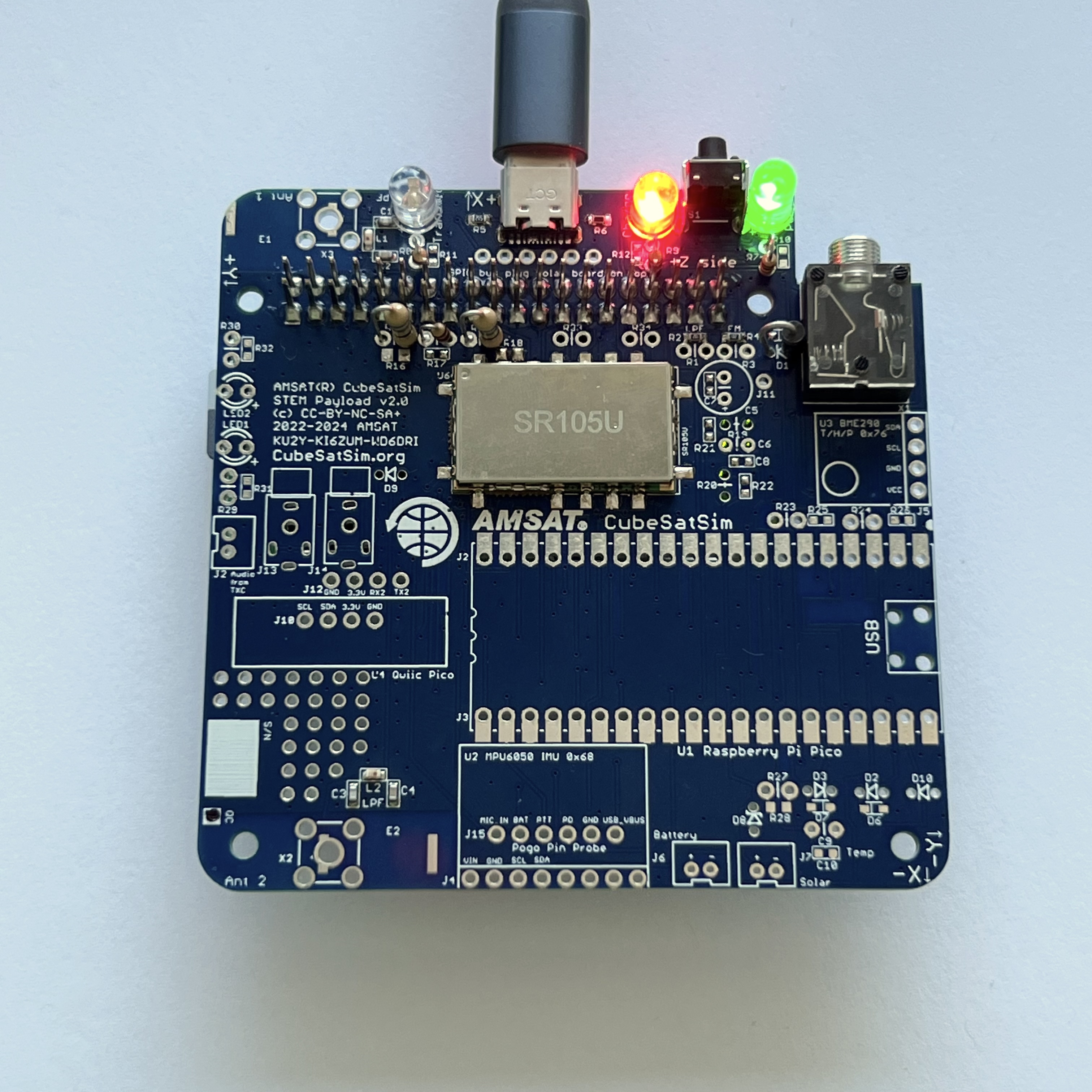
If the LED doesn't illuminate, it might mean there is a problem with the green LED LED3 or resistor R7 or that the CubeSatSim software isn't running.
Transmit LED Test
With the Pi plugged into the main board and the power cable plugged into the Pi micro USB port, after booting, the CubeSatSim software will run. When the CubeSatSim is transmitting, the blue Transmit LED will be illuminated, occasionally blinking. This indicates that the CubeSatSim is transmitting.
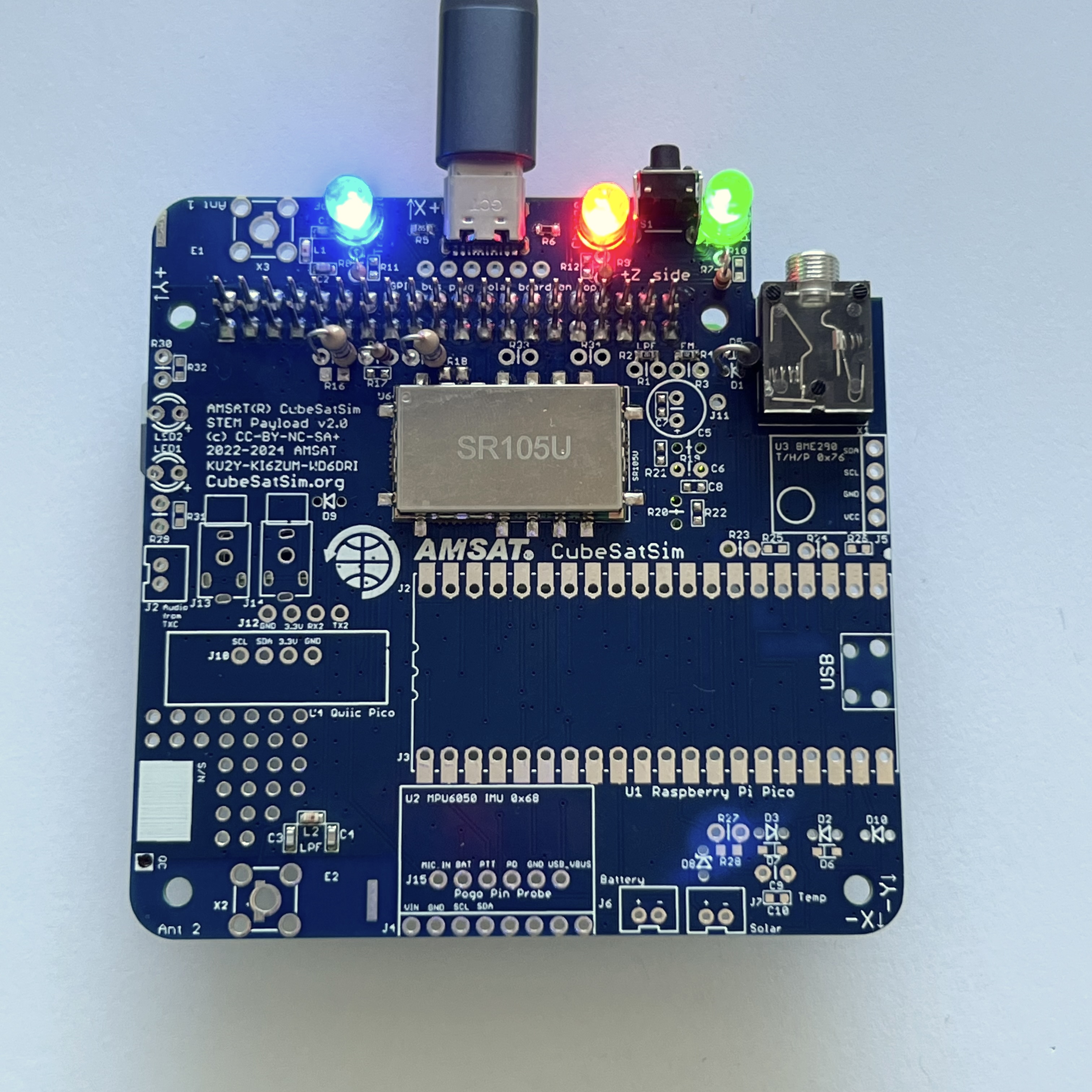
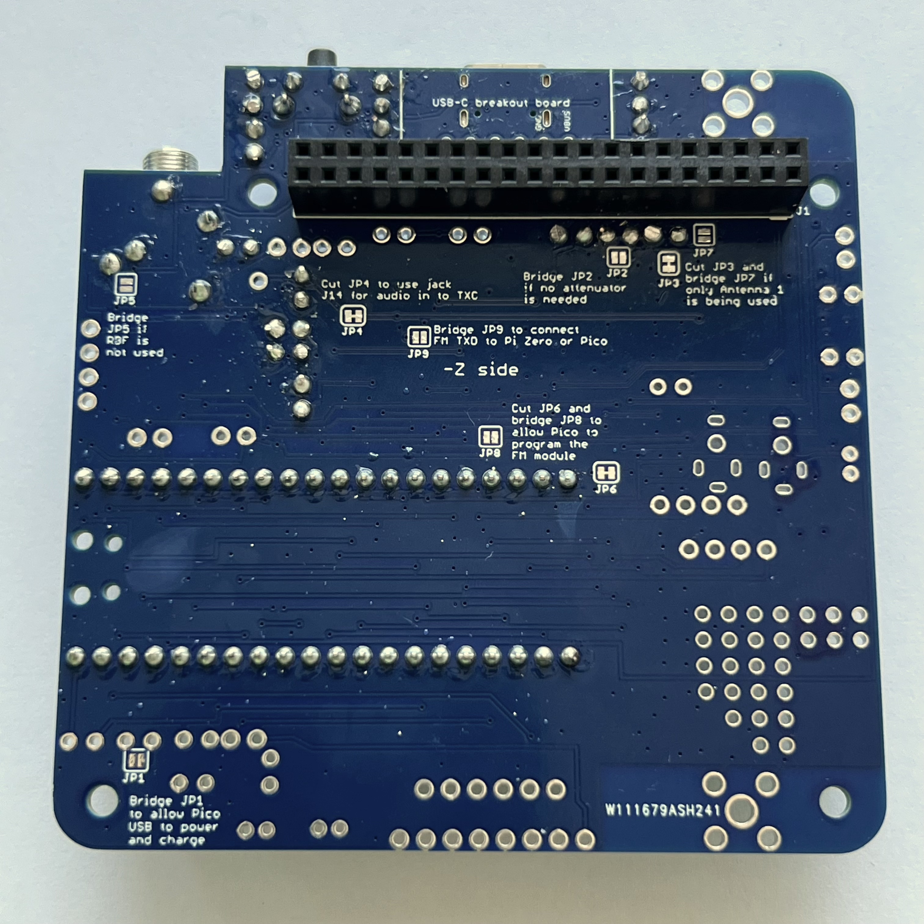
If the blue LED doesn’t illuminate, it might mean there is a problem with the blue LED LED4 or resistor R8 or the CubeSatSim software. If it only illuminates once, it might mean that the Low-Pass Filter is not detected by the presence of either resistor R1 or R2 - check this resistor.
Transmit Test
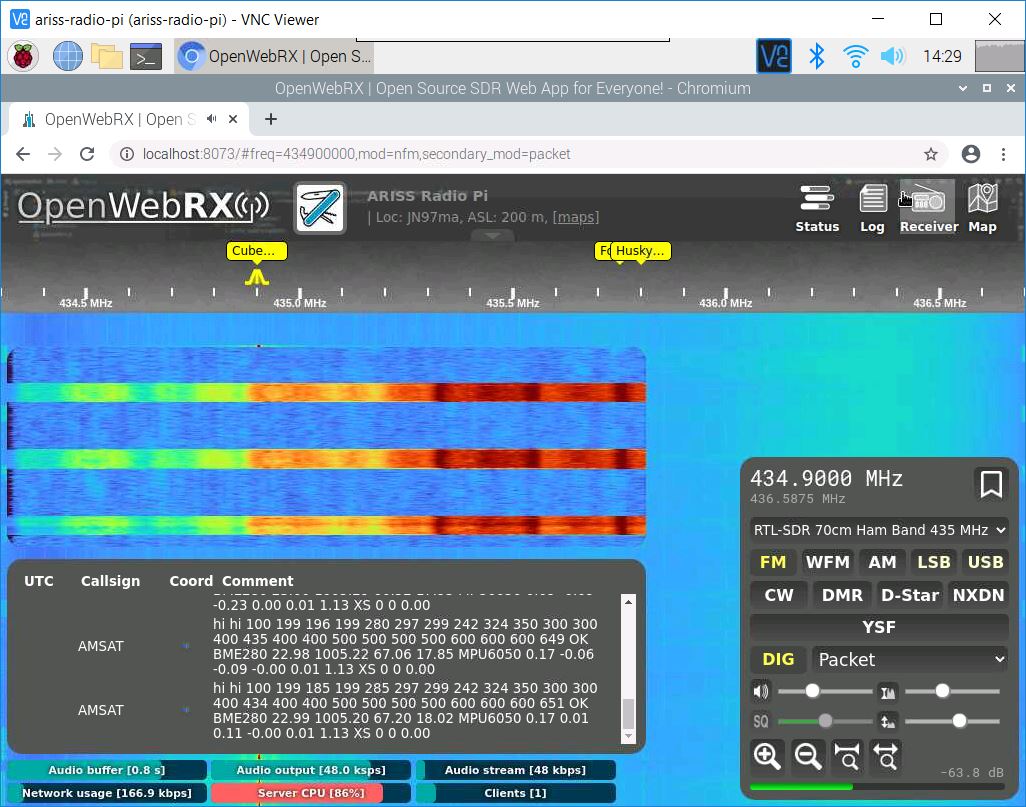
If the blue LED is illuminated or blinking on and off, you can tune your radio or SDR to 434.9 MHz (+/- 15 kHz) to see and hear a carrier signal. You don't have an antenna yet, but a close by radio will pick it up. If you have your FoxTelem ground station working (the Ground Station instructions are here), you can try to decode frames in FSK mode.
If your blue Transmit LED is illuminated but you don't see a signal, check your antenna on your radio or SDR, and the gain and frequency on your SDR or radio. Or there may be a problem with the CubeSatSim software, in particular the rpitx library.
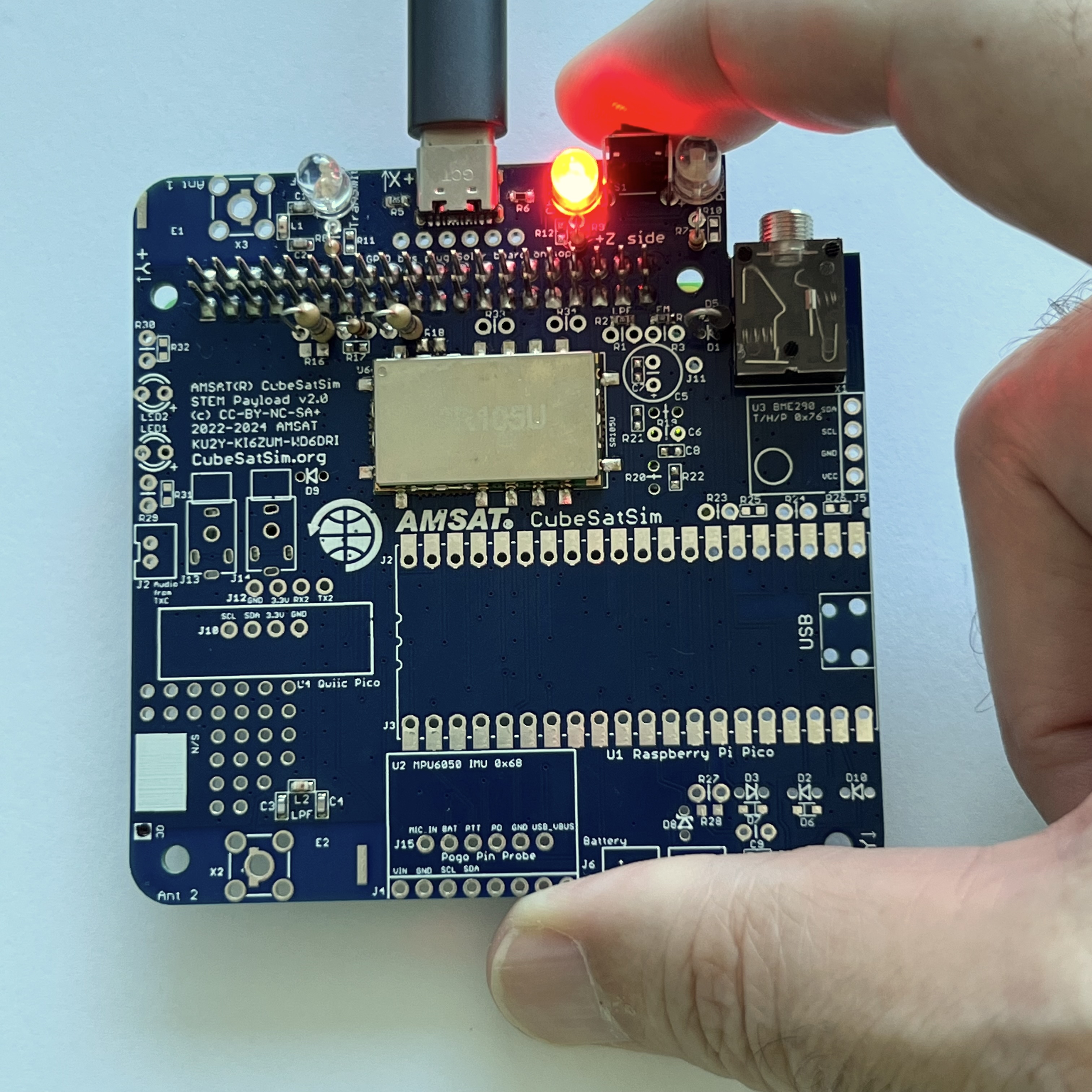
Push Button Test
Press and hold the pushbutton. The green LED will blink once, then twice, three times, four times, then five times, then it will blink three times slowly. Immediately release the pushbutton when it blinks slowly and the Pi Zero 2 computer will shut down and the transmissions and the blue LED will stop blinking.
RBF Switch Test
After completing the Push Button Test, insert the RBF pin. Only the red LED will be illuminated.
Unplug the RBF pin and the Pi Zero 2 will boot up and eventually the green LED will turn on the blue LED will start blinking. Hold down the push button again until the Pi Zero 2 shuts down. Then put the RBF pin back in.
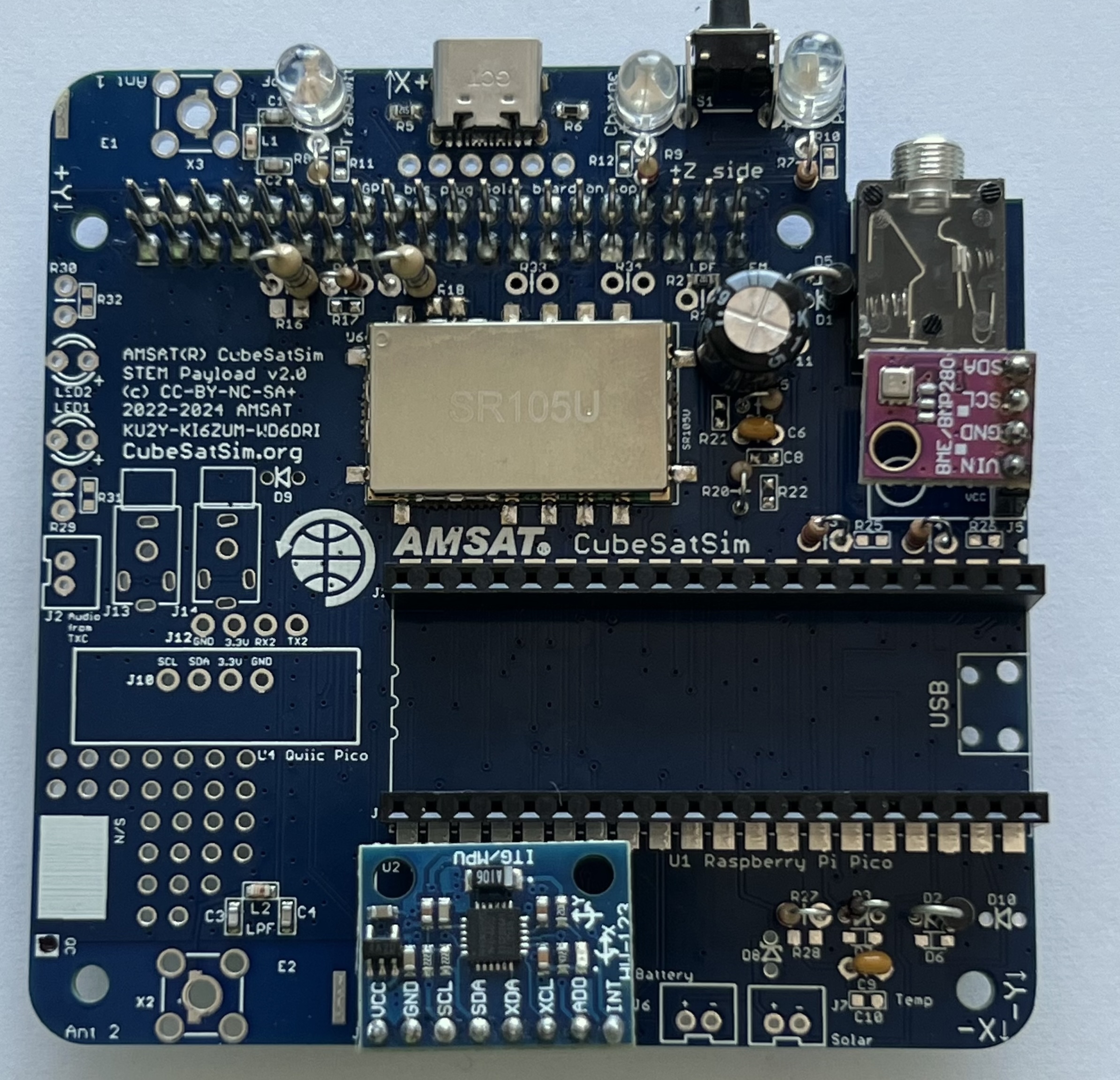
4.2 Build
Video
Here is a video of this step.
If all your test results are "nominal" (expected results), you can continue your build after shutting down the Pi as described in the Power Button Test (by holding the push button until the green LED blinks slowly then releasing) and unplugging the Pi from the board.
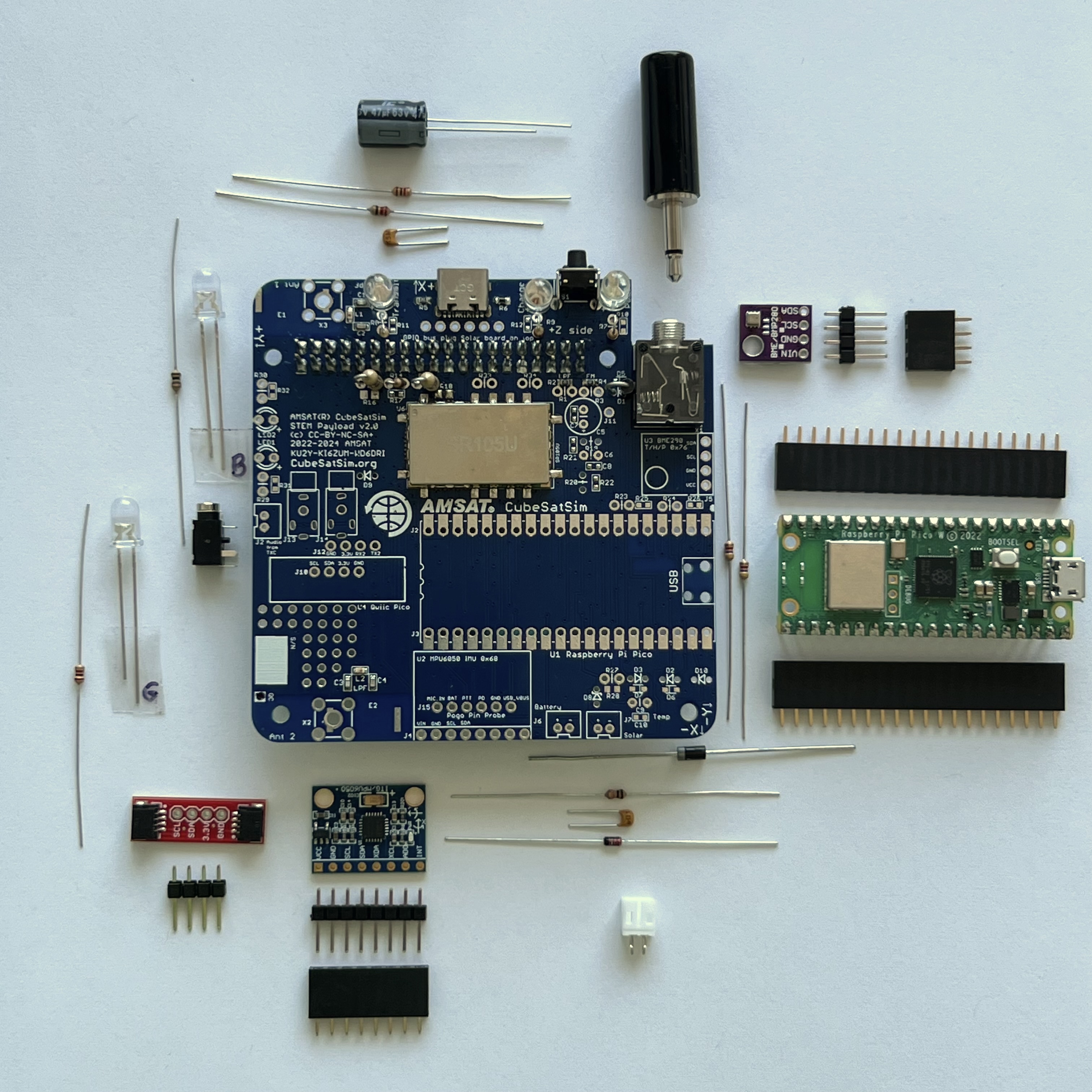
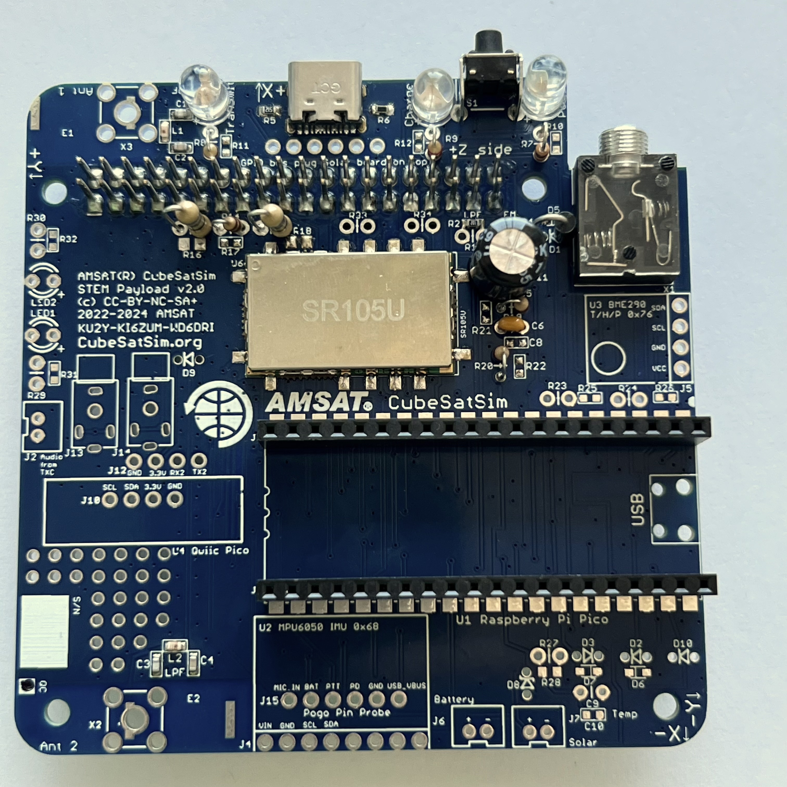
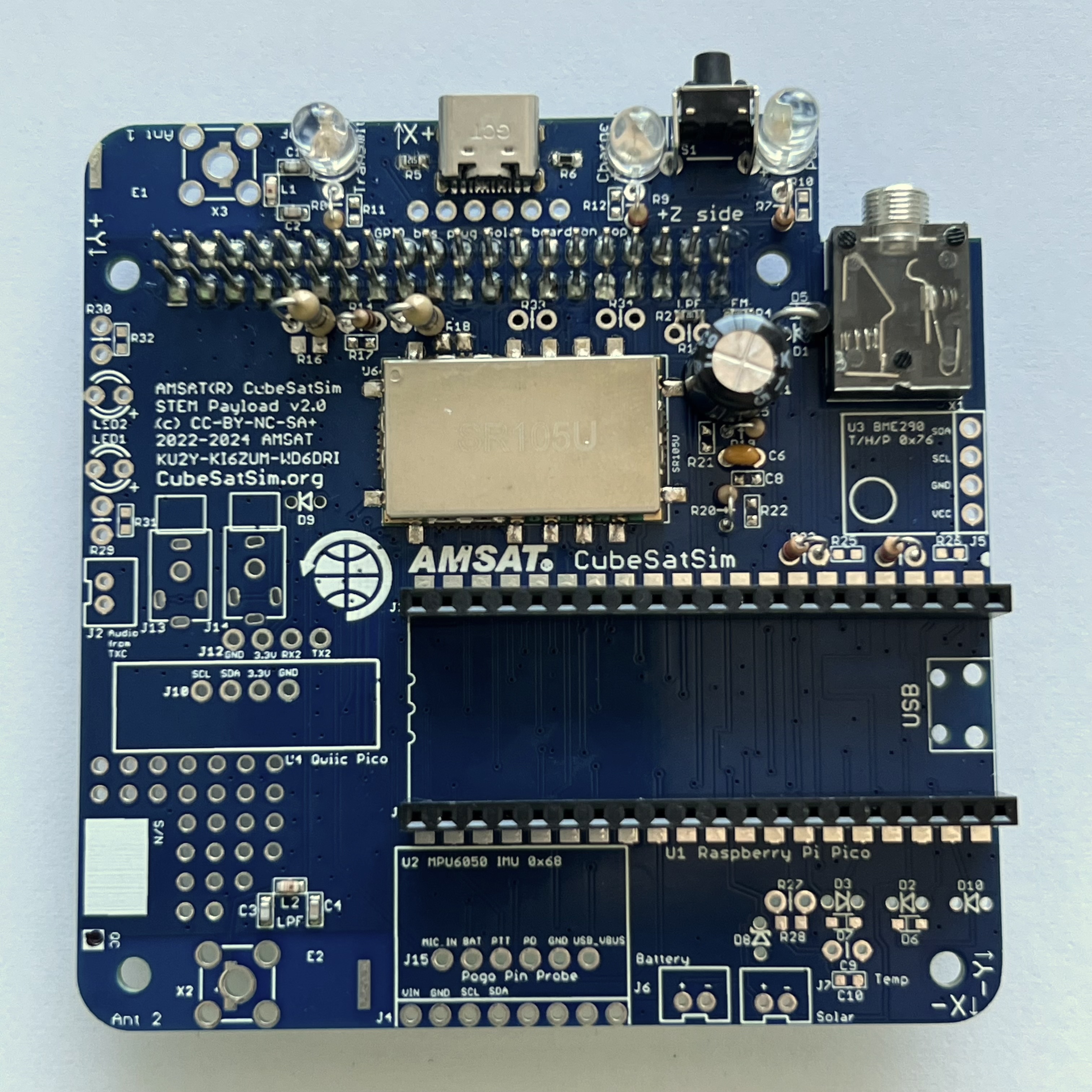
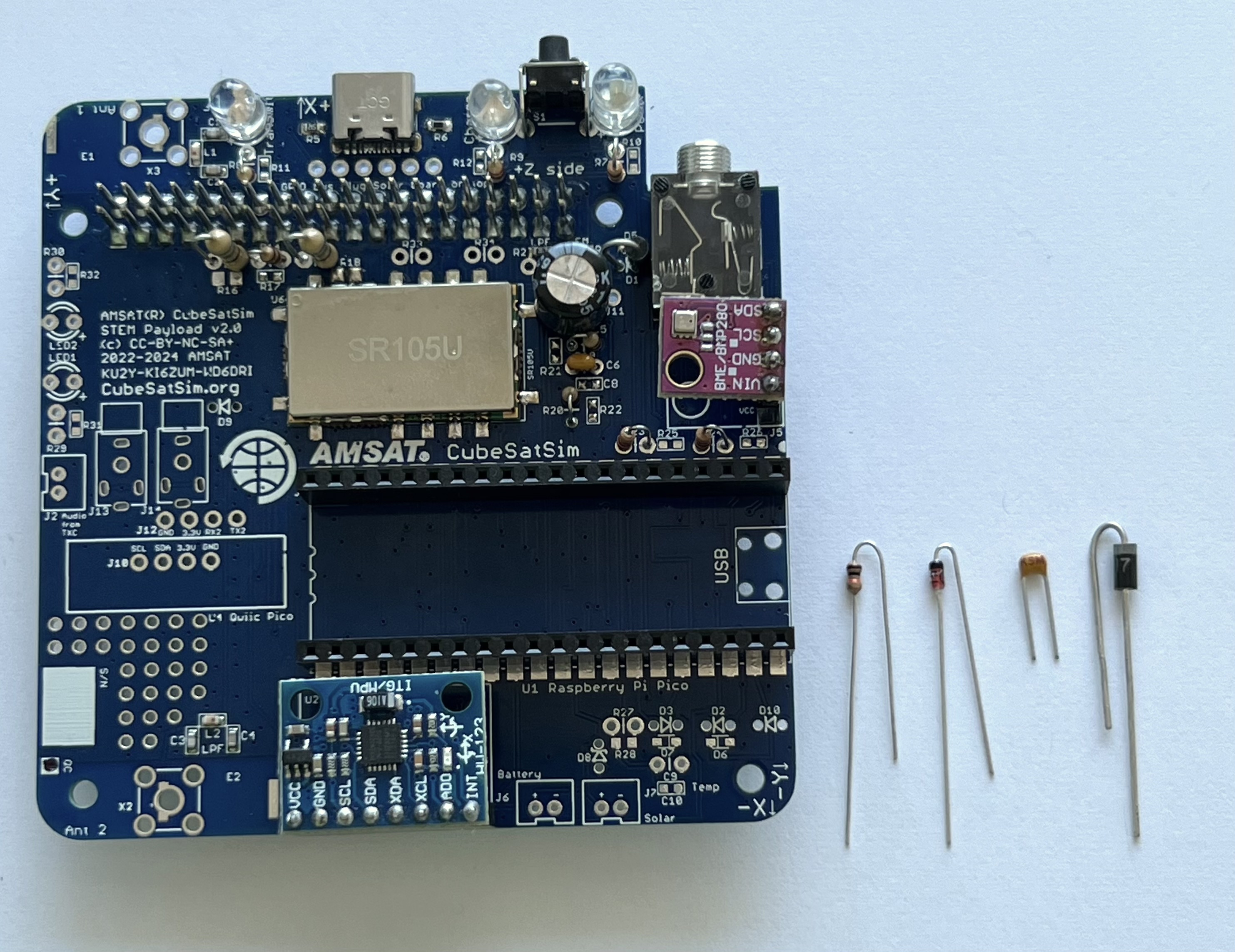
Here are components installed in this step, as described in the BOM https://CubeSatSim.org/bom
You should unplug the Pi Zero 2 from the board before continuing with the assembly.
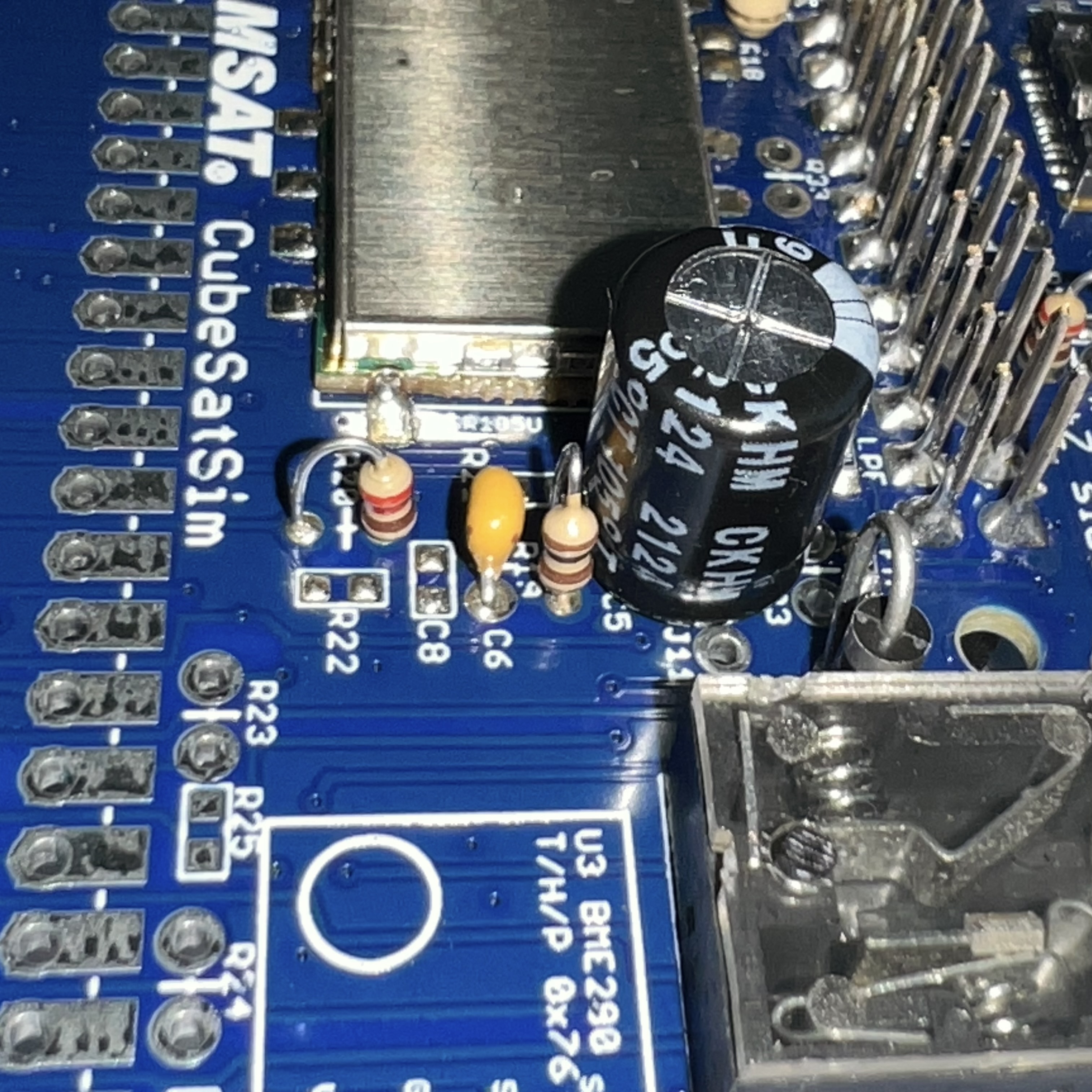
First, install the audio low pass filter that feeds the PWM (Pulse Width Modulation) audio signals into the FM Transceiver module with 47uF capacitor C5 (can), 100nF capacitor C6 (small yellow capacitor), 220 Ohm resistor R20 (color bands red red brown) and 100 Ohm resistor R19 (color bands brown black brown):
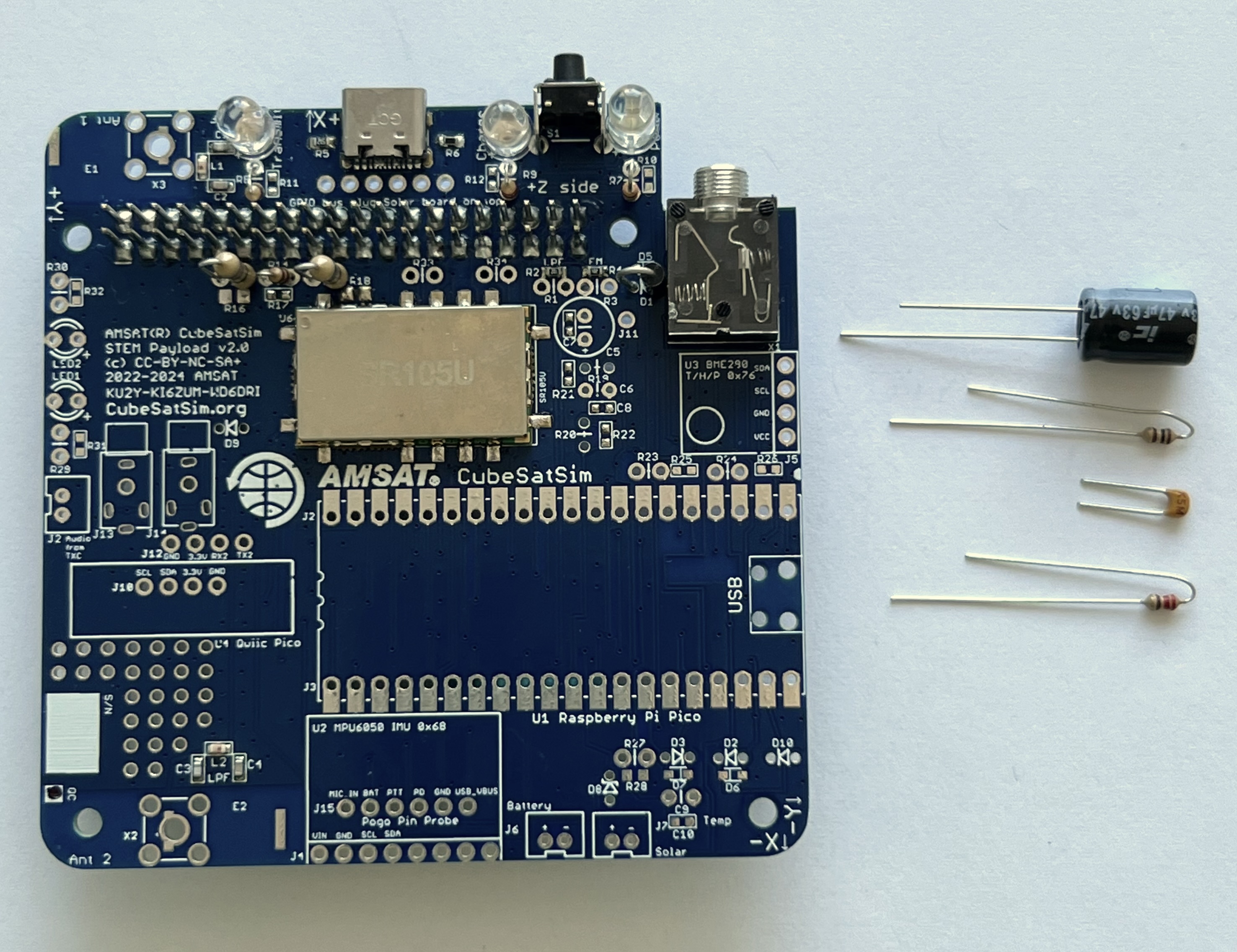
The electrolytic capacitor C5 has polarity - the negative lead (the shorter one in the photo) is marked with a white -. In the photo above and on the PCB, the positive side is marked with a +.

Here is a closeup showing the parts:
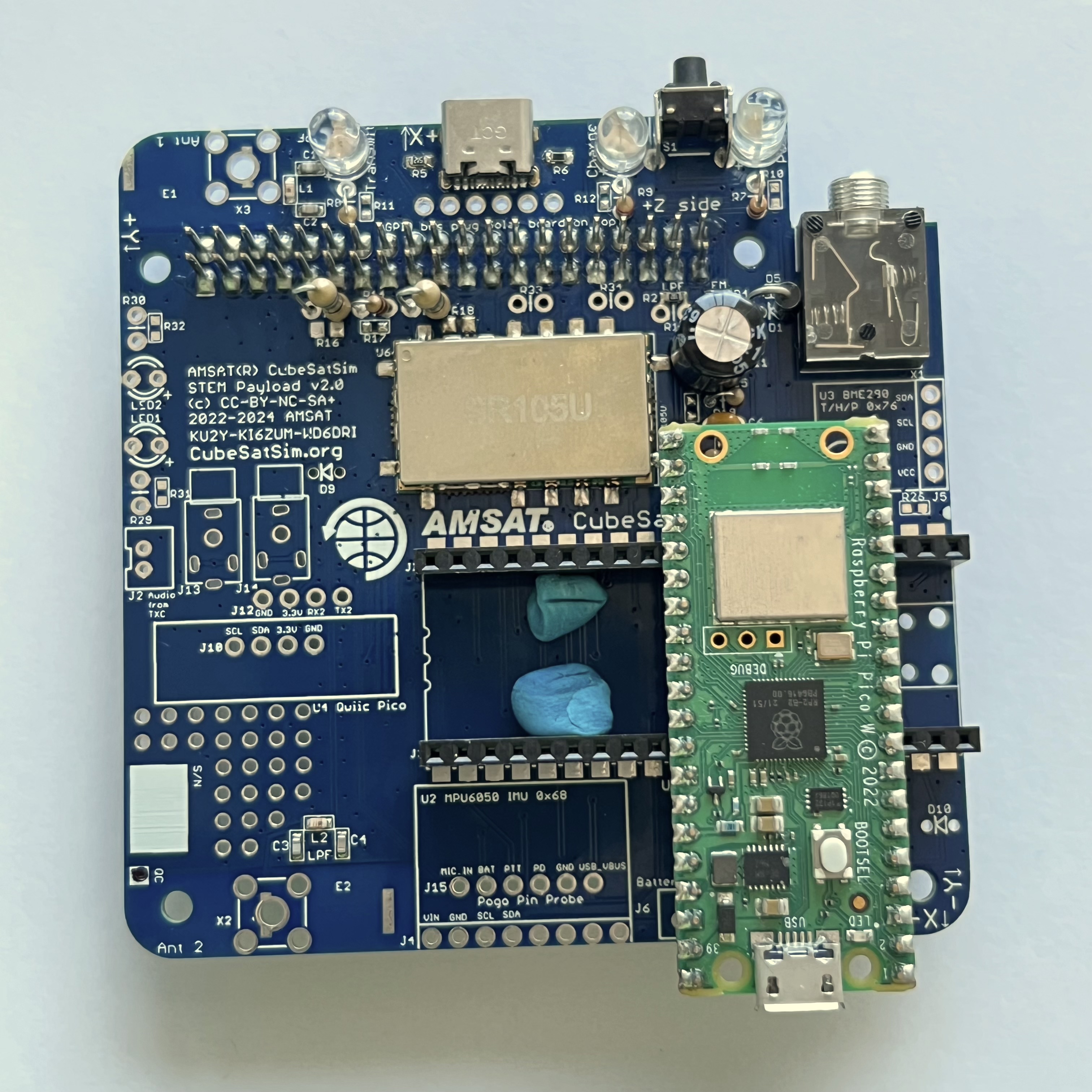
Next, we will install the female sockets J2 and J3 used to mount the Raspberry Pi Pico microcontroller U1. If your Pico doesn't have the male pin headers installed, you will need to solder them in.
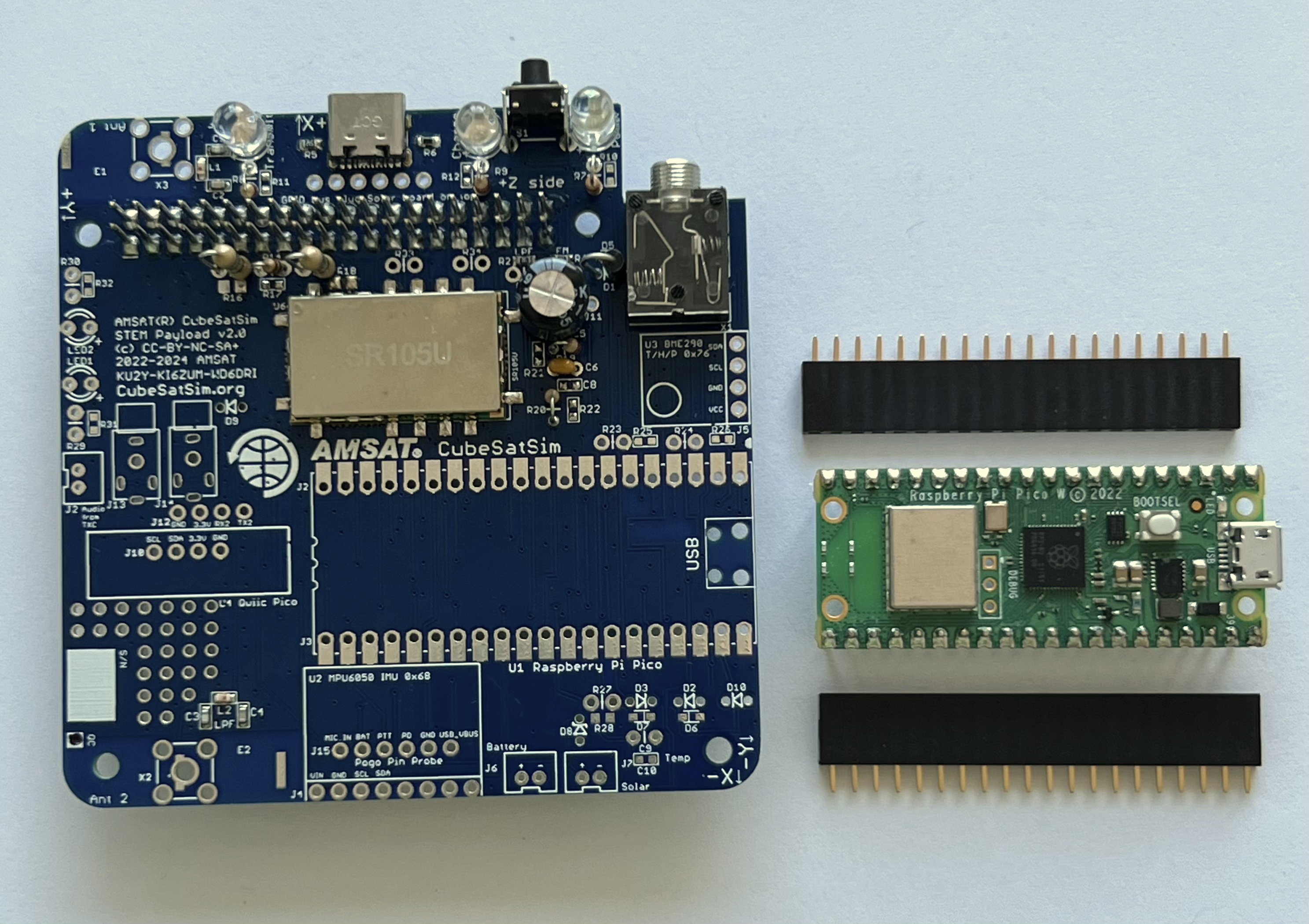
The spacing and alignment of the female sockets is important, otherwise the Pico won't plug in. You can use the Pico itself at right angles to ensure they are spaced correctly and at right angles to the PCB, or you could use the 1x8 pin header from the MPU 6050 board J4.
First solder only one pin on each header and double check to make sure it is installed correctly. Look at it sideways to make sure there is no gap - this photo shows a tiny gap which is fine:
Here is the bottom of the PCB with all the pins soldered:
Here is the board with the headers installed ready to plug in the Pico:
The FM modes can now be tested with the help of the Pi Zero 2 with a programmed SD card. If you haven't completed these steps, you can find them here: Pi Zero 2 and Pico Software Install Instructions

Plug the Pi Zero 2 into the bottom of the PCB. Plug in the powered USB-C power cable and the Red charging LED should illuminate. The Green Power LED will illuminate after a few seconds. Then the Blue LED will illuminate and go on and off:

Push Button Test
With the Pi plugged into the main board and the power cable plugged into the Pi micro USB port, after booting, the CubeSatSim software will run. When the push button is pressed and held, the green LED should blink rapidly in this sequence: 1 quick blink, 2 quick blinks, 3 quick blinks, 4 quick blinks, 3 slow blinks. Releasing the button after one of the quick blink sequences will put the CubeSatSim in that mode, and the green LED will stop blinking. For example, in this video, the push button is released after the 3 blinks, so the CubeSatSim is in Mode 3. http://countingfromzero.net/amsat/v1/blink.MOV The modes are: 1: APRS, 2: FSK, 3: BPSK, 4: SSTV, 5:CW.
- When pressed and immediately released, the Pi should reboot after about 30 seconds.
- When pressed and held until the green LED starts to blink slowly (see above for the LED blink sequence), the green LED will then blink slowly three times, then the Pi will shutdown (the green Power and blue Transmit LEDs will go out, then the tiny green LED on the Pi will flash rapidly for about 10 seconds then go out). You can release the button as soon as the LED starts blinking slowly. This video shows the button shutting down the Pi: http://countingfromzero.net/amsat/v1/shutdown.MOV After the Pi is shutdown (no LEDs are on or blinking), you can safely disconnect the USB power cable and unplug the Pi from the board to continue the build.
If the green Power LED doesn’t blink, there might be a problem with the push button switch S1 or with the pi-power-button software.
If you don't hear anything or see anything for the FM modes (APRS, SSTV, and CW), try listening on 450.000 MHz for the signal. If you hear the signal there, it means the FM Transceiver module hasn't had its frequency set to 434.9 MHz by the Pi Zero 2 software. Try powering down everything and then powering up again.
Continue Build
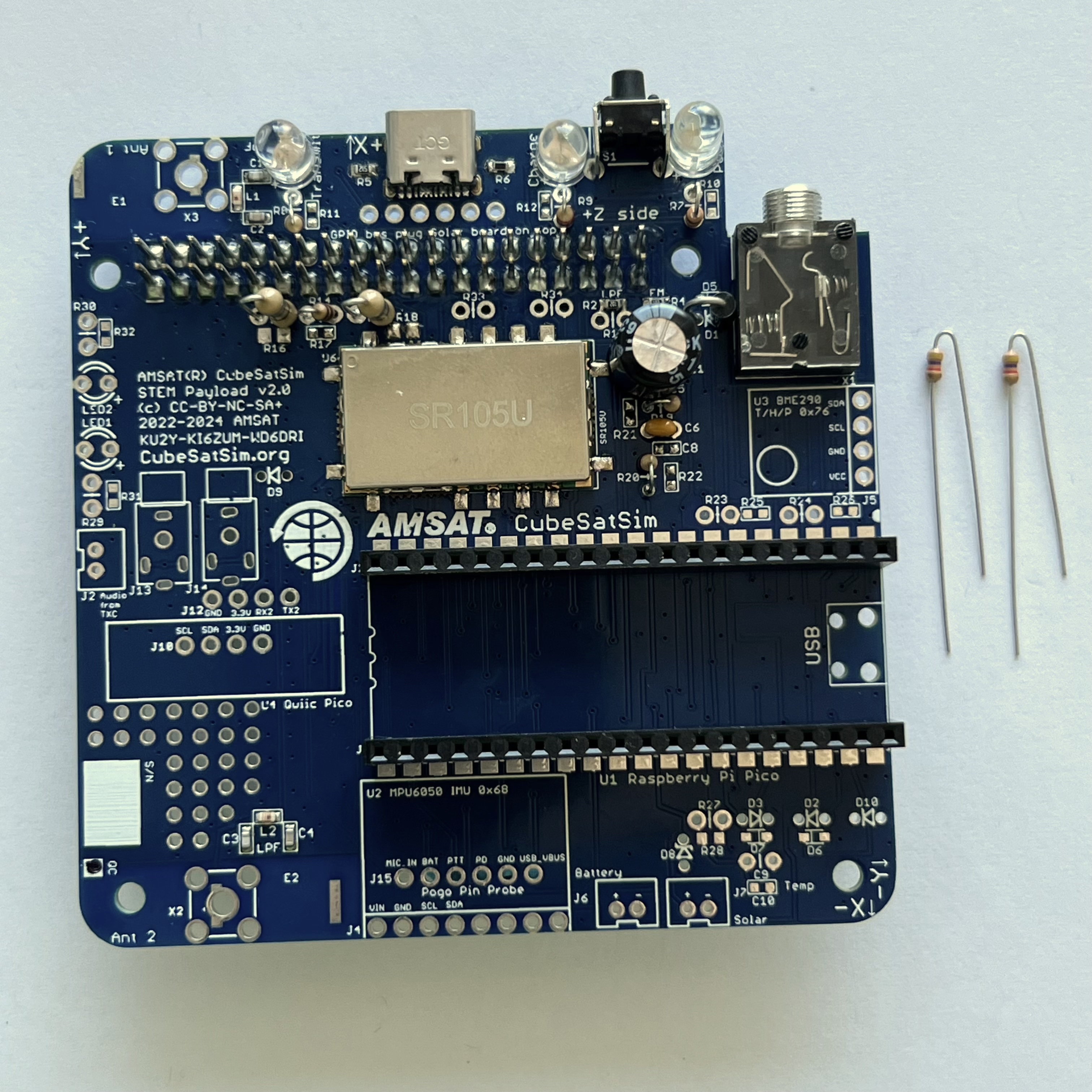
Then mount the two 4.7k Ohm resistors R23 and R24 (yellow violet red color bands):
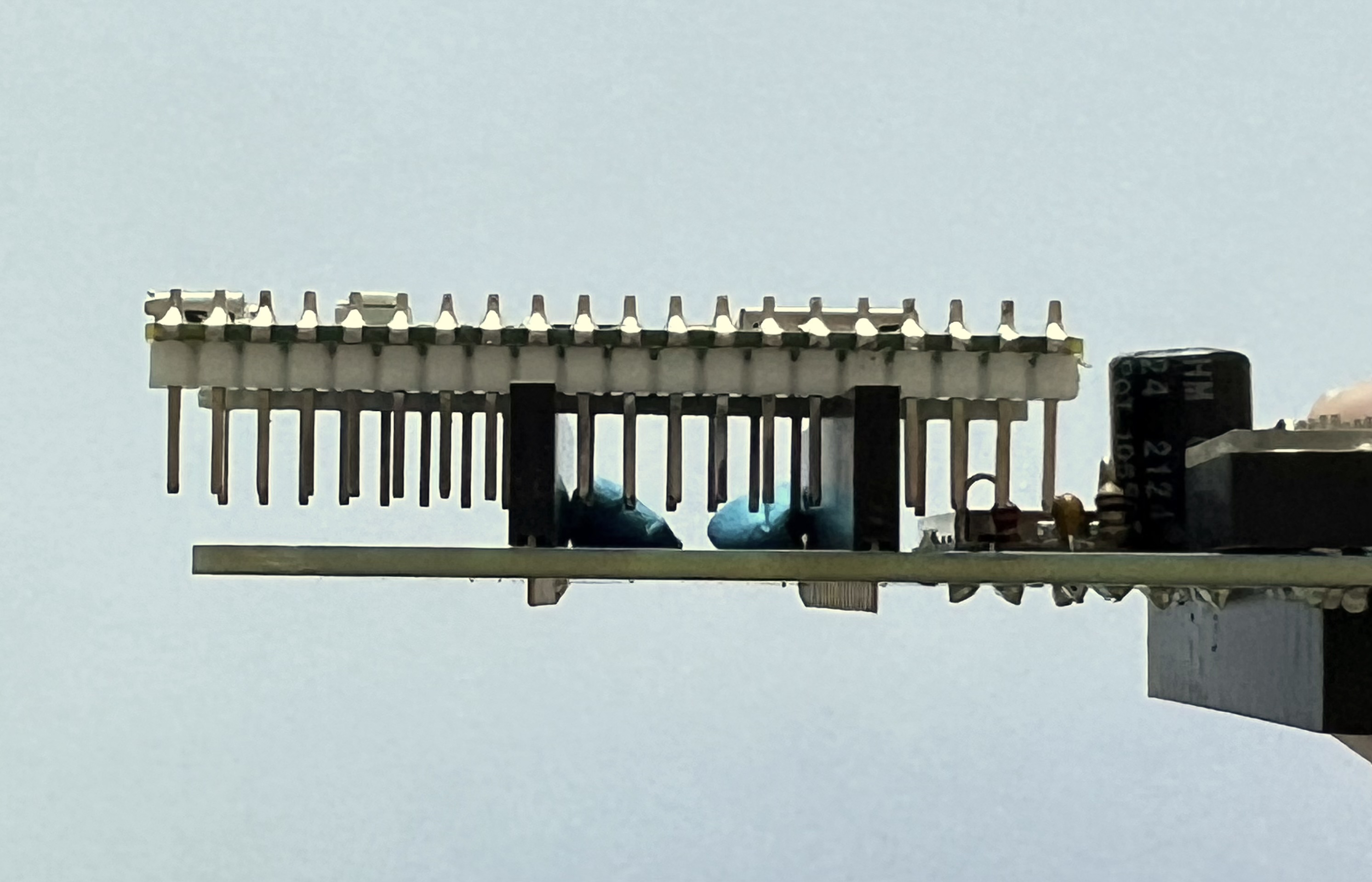
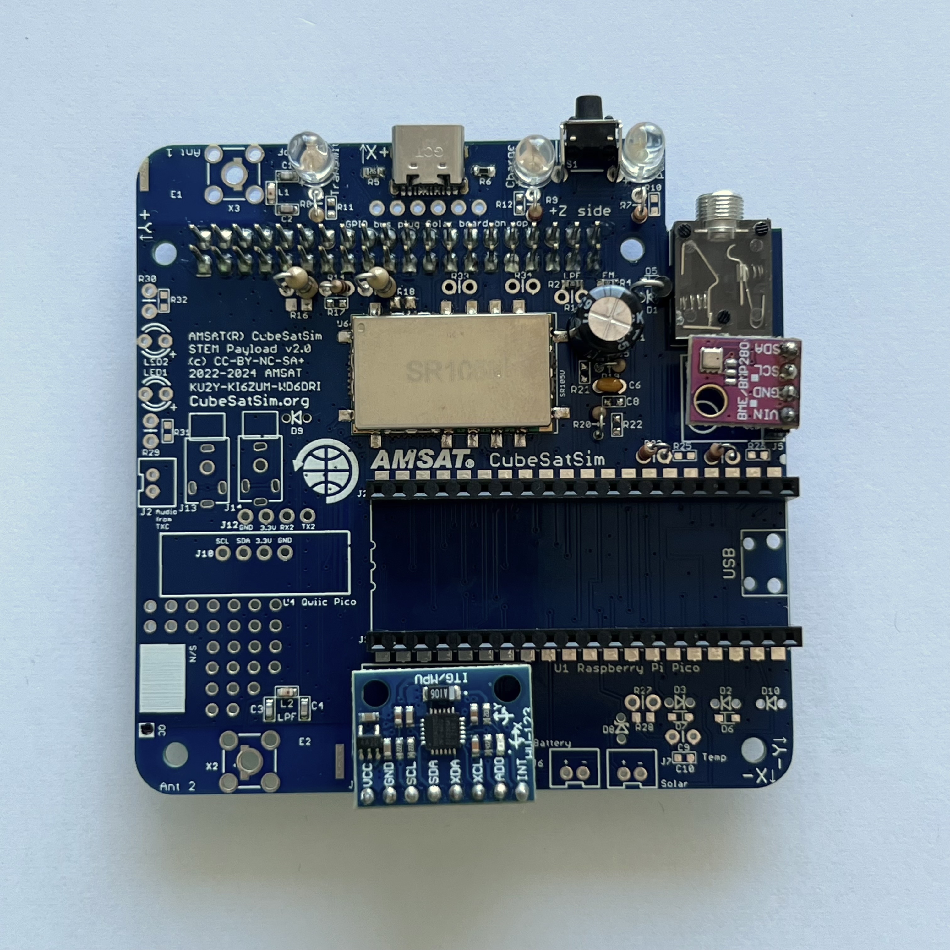
Next we will mount the BME280 sensor (small purple board) J5 and the MPU6050 Gyro and Accelerometer sensor (larger blue board) J4. They can be mounted directly on the board or on female sockets for more flexibility.
They are mounted with female sockets:
First solder the female sockets, making sure they aren't tilted. Blue putty can be used to hold them in place during soldering.
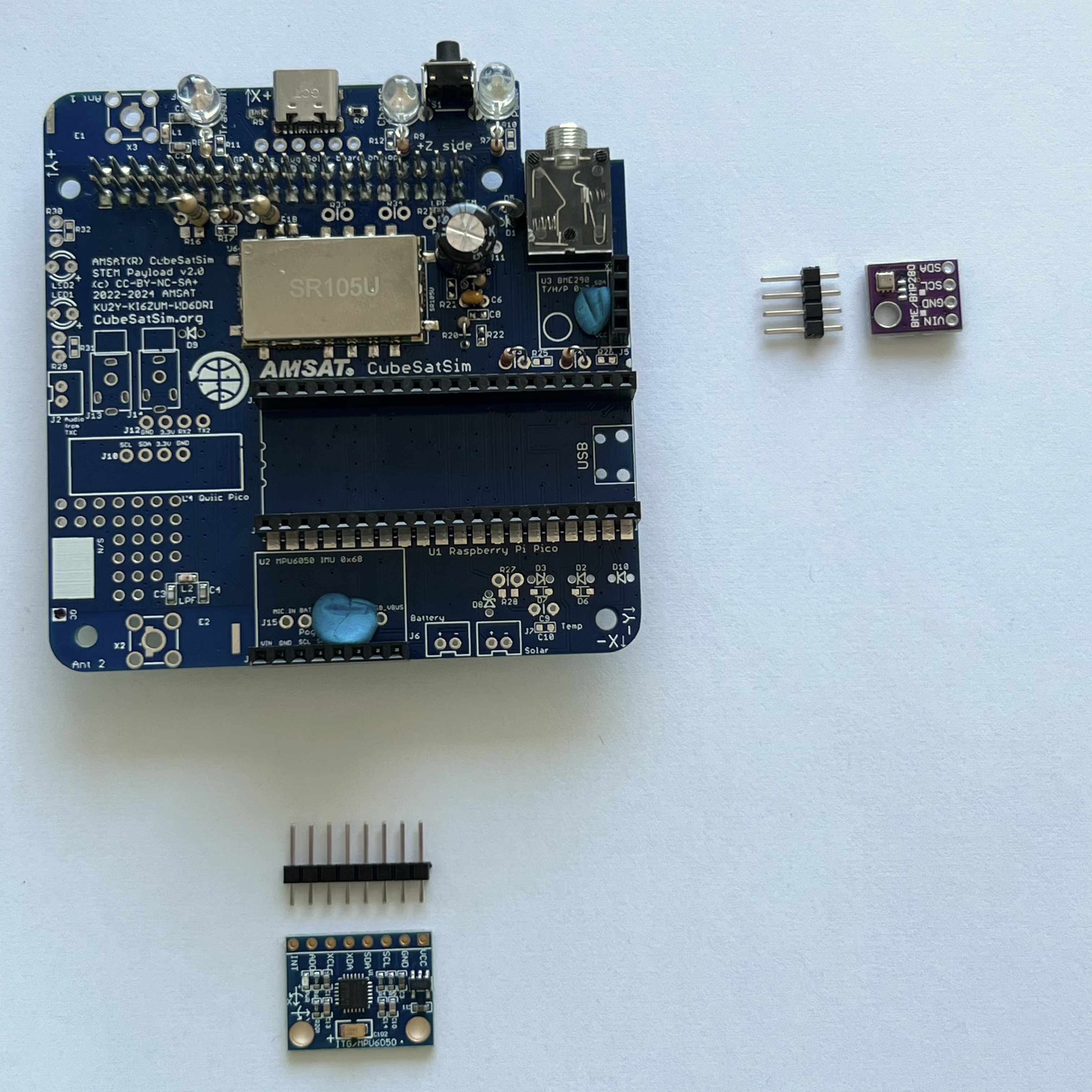
Solder one pin on each socket, double check, then solder the rest.
Insert the pin headers into the sockets, long pins into the sockets, then place the sensor boards on top. Blue putty can be used to hold them horizontal to the board.
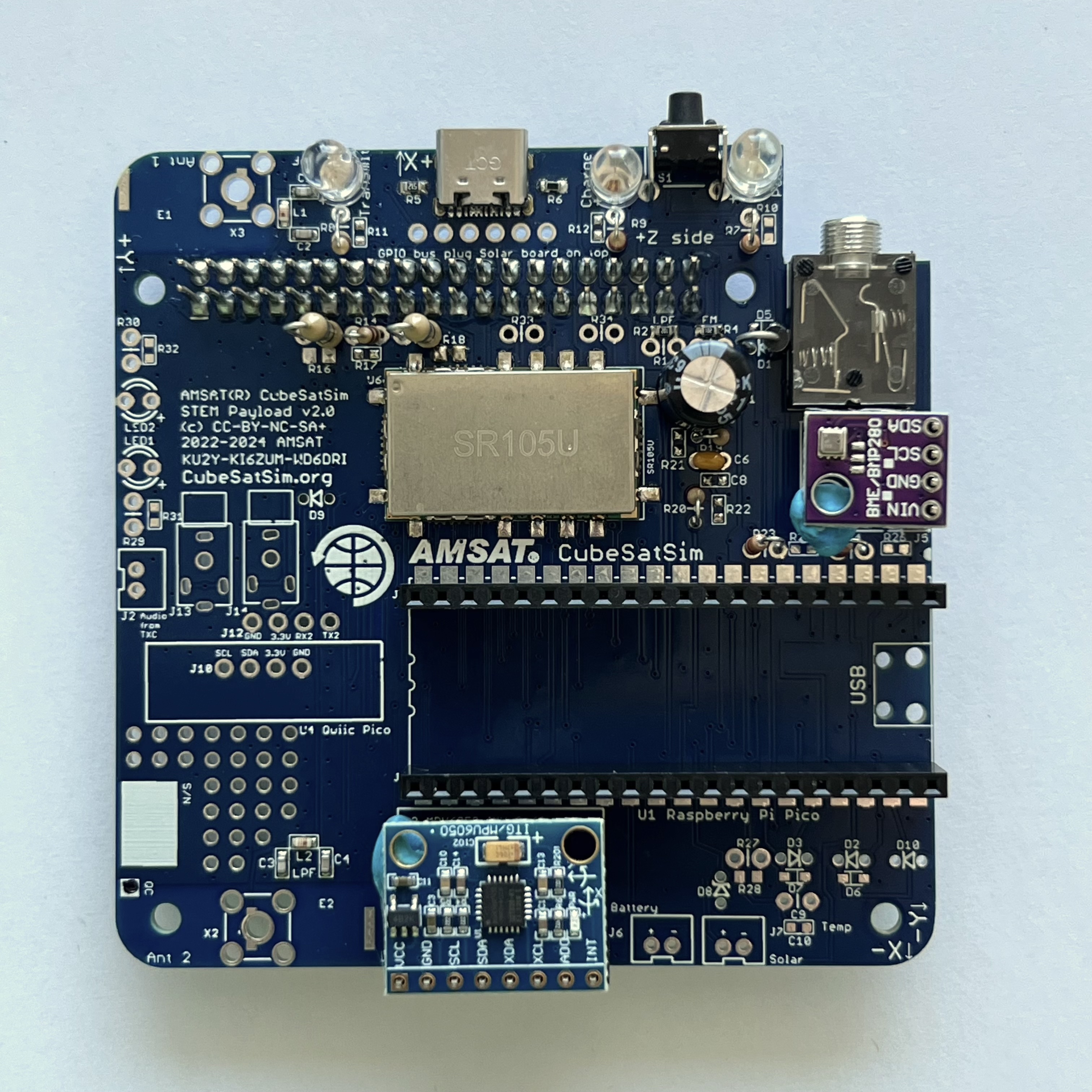
IMPORTANT: make sure the purple BME280 is not upside down. The top has the BME sensor chip (small metal can). The circular hole in the board should be to the left.
Solder the pins:
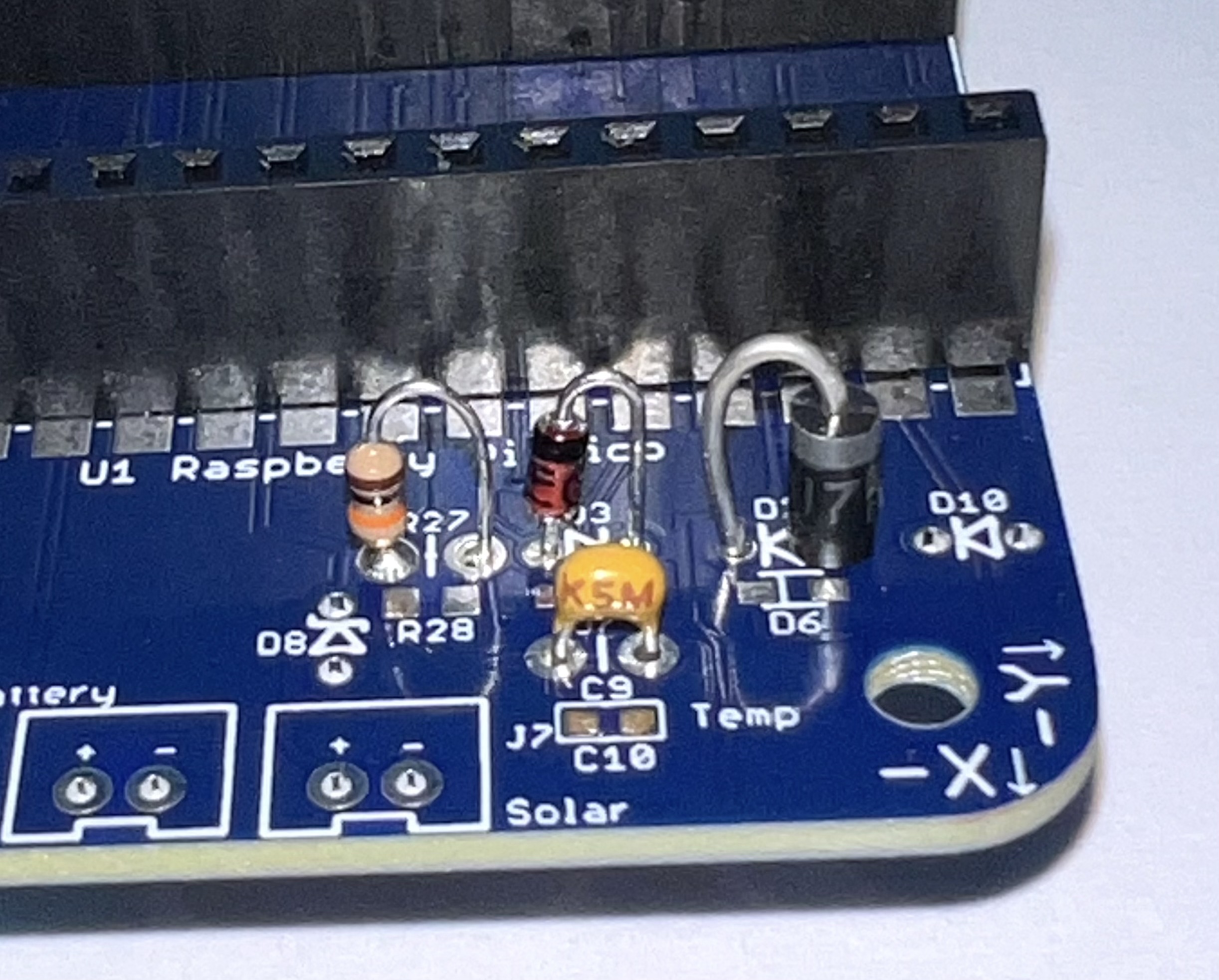
Next, solder these four components on the bottom right of the PCB:
- 10k resistor (brown black orange color bands) R27
- 100nF capacitor C9 (small yellow capacitor)
- 1N5817 diode D2 (black device with a white band on one side to mark polarity)
- 1N4148 diode D3 (has a glass case with the numbers "41" and "48" written on it and a black band to indicate polarity
Here's the polarity of the diodes:
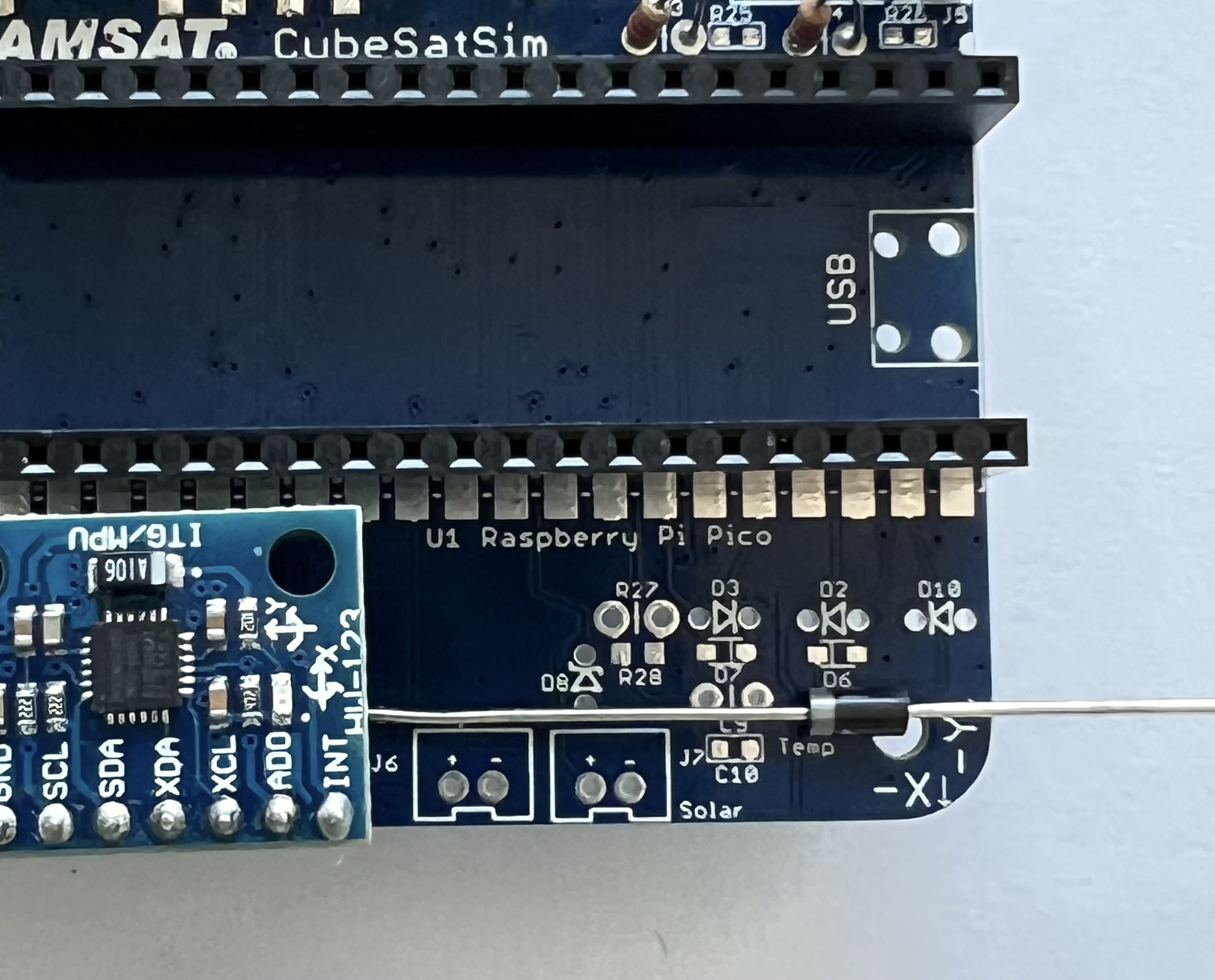
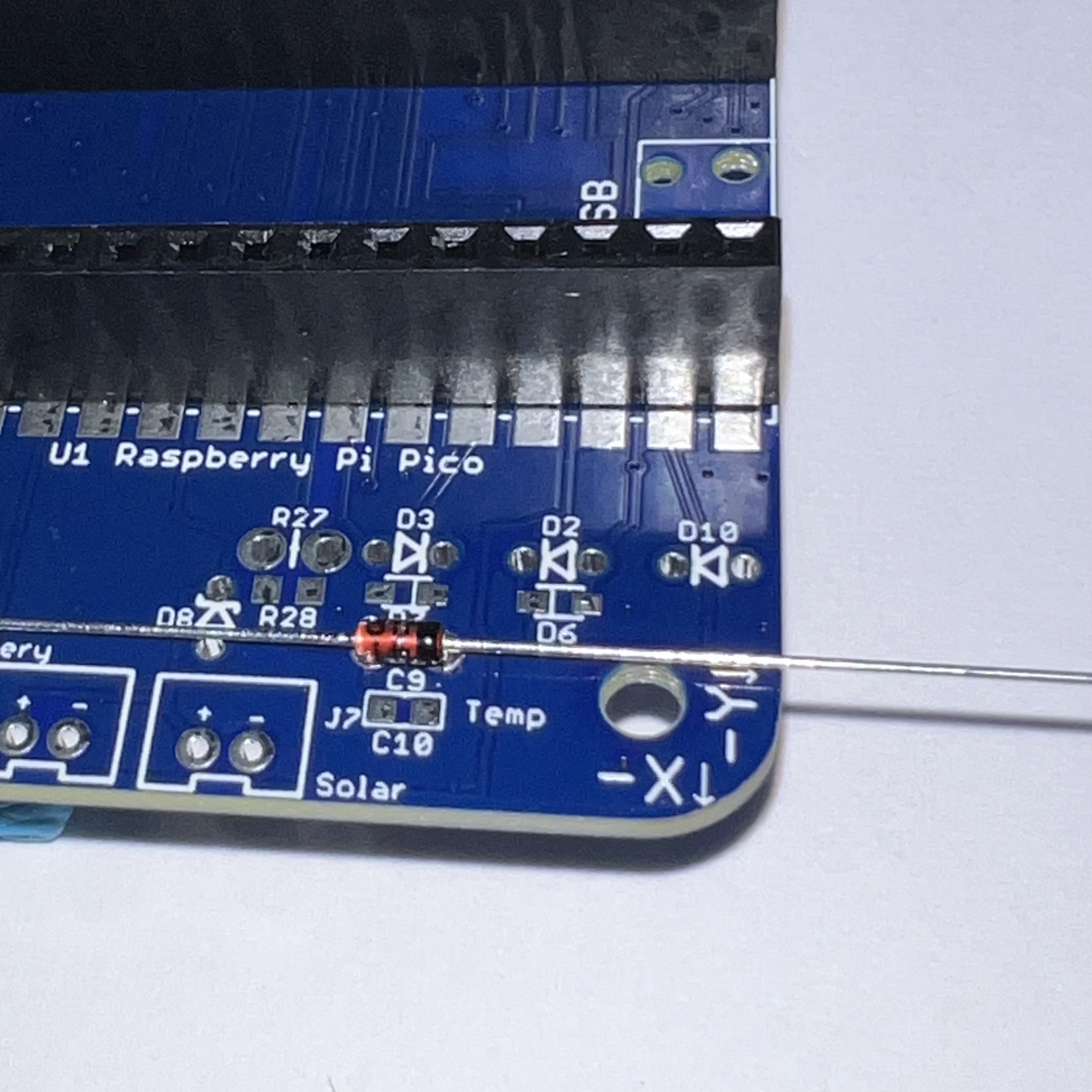
All the diodes, along with all the resistors on the board are mounted vertically. Bend over one lead on the diode and insert, making sure the polarity of the diodes is correct before soldering them.
Here's all four parts ready to install:
Solder the leads on the bottom of the PCB.
Then trim the leads, being careful to wear safety glasses and putting your finger over the end so it doesn't go flying.
Here's after they are installed:
Here is a closeup:
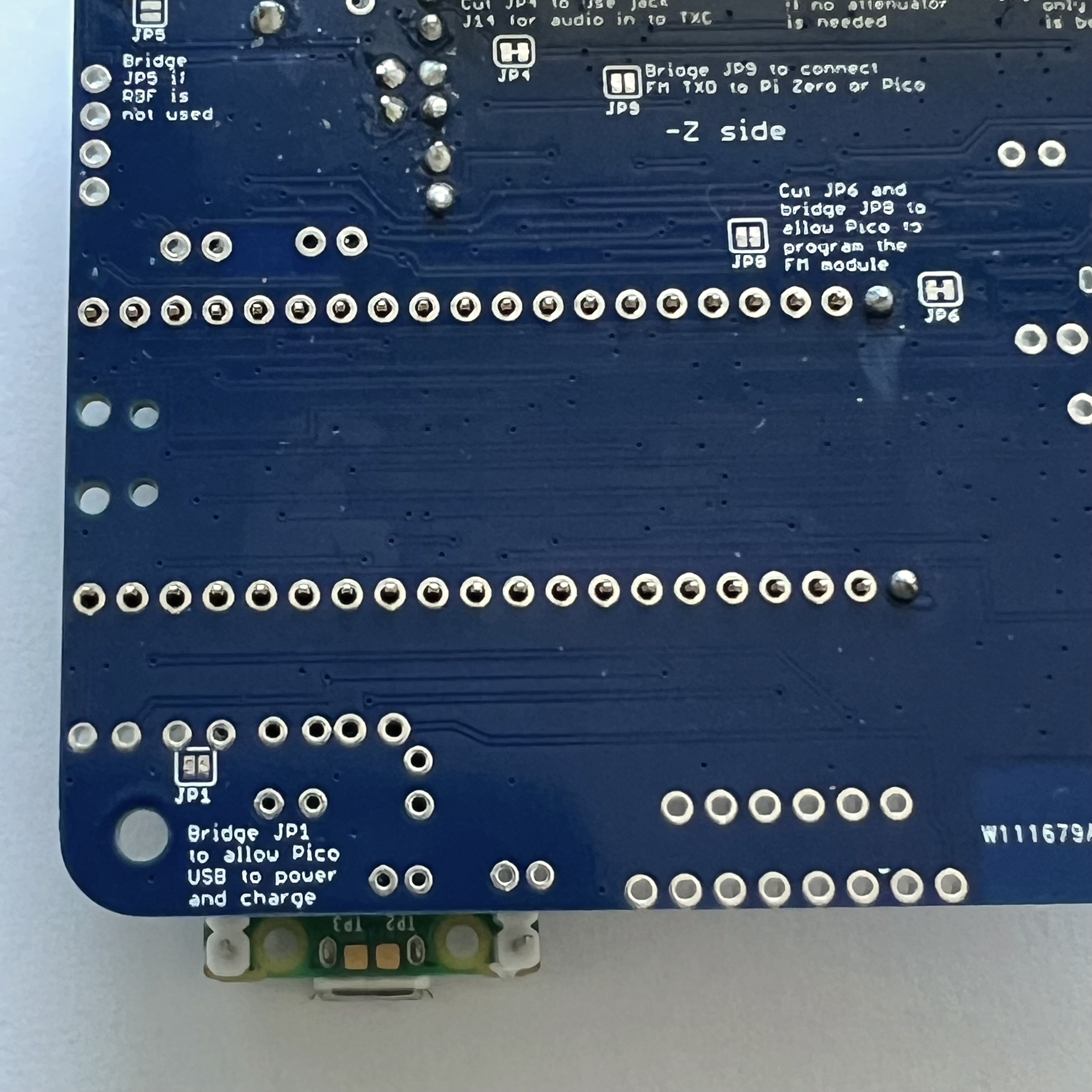
Install the JST connector J7 which is labeled "Solar" since the JST jumper cable will connect it to the Solar Board. The other JST connector J6 labeled "Battery" is used if no solar panels are used and the Battery Board will be connected here.
Here is a closeup showing that the slot should face the edge of the PCB for correct polarity. Some JST connectors snap into the board. If yours do not, then I recommend a drop of super glue gel or other adhesive prior to soldering:
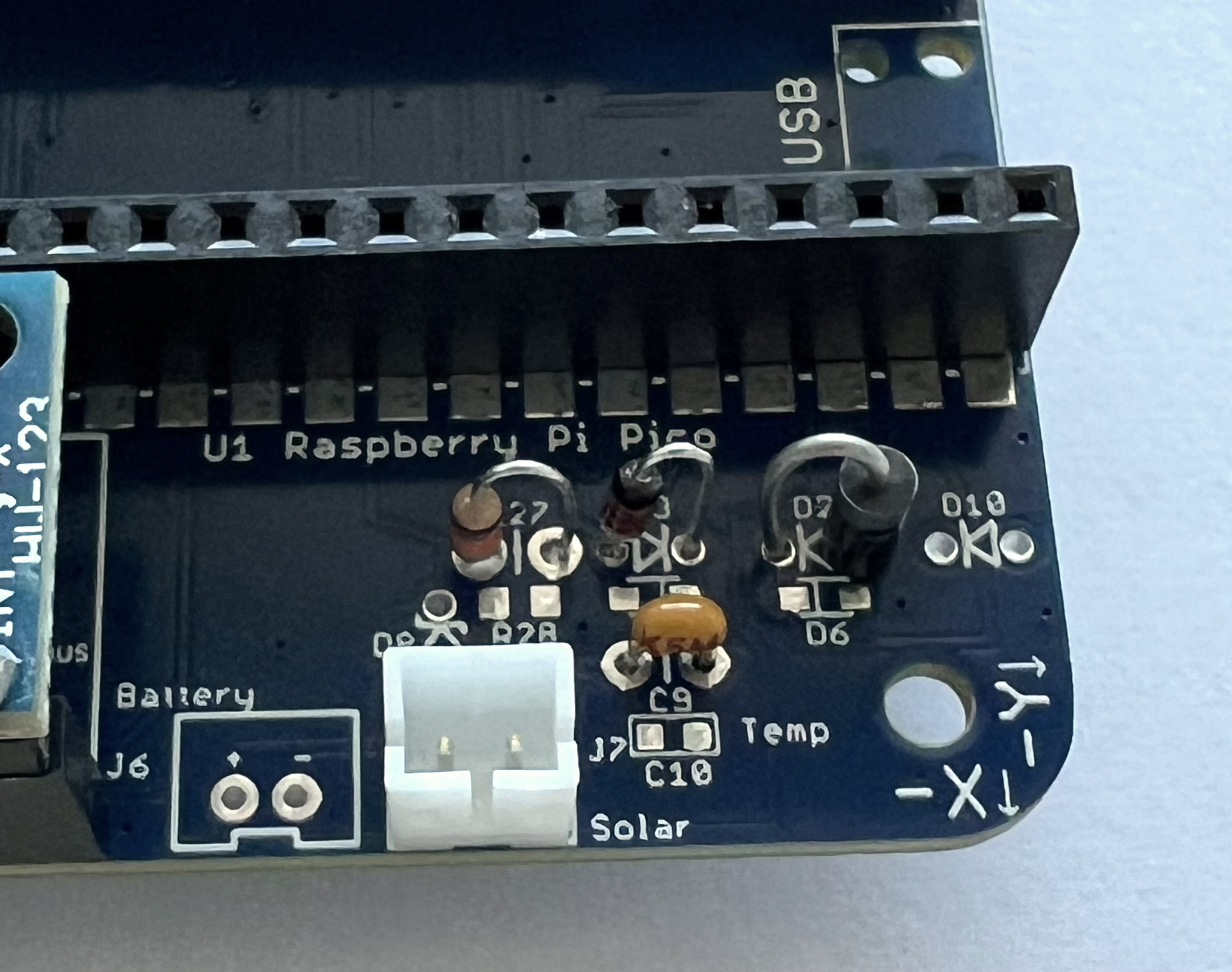
Here's how it looks installed:
Then install the white LED2 and 1k Ohm R30 (brown black red color bands). LEDs need to be installed with the correct polarity (one lead is + polarity and the other lead is - polarity) or it will not illuminate. The longer leg on the LED is the '+' lead and should be away from the edge of the PCB. Also, if you look at the LED lens from the top, it is circular but there is a flat side that marks the '-' side. So the flat side of the LED should be towards the edge of the PCB.
The longer lead of the LED is the positive and matches the '+' on the PCB. This LED and the yellow one next to it are turned on and off by the microcontroller.
Then install the yellow LED1 and 1k Ohm R29 (brown black red color bands). The longer lead of the LED is the positive and matches the '+' on the PCB.
Here are all the resistors and LEDs installed:
Next, install the Qwiic connector (red board) and 1x4 male pin header J10 for adding more I2C sensors to the board:
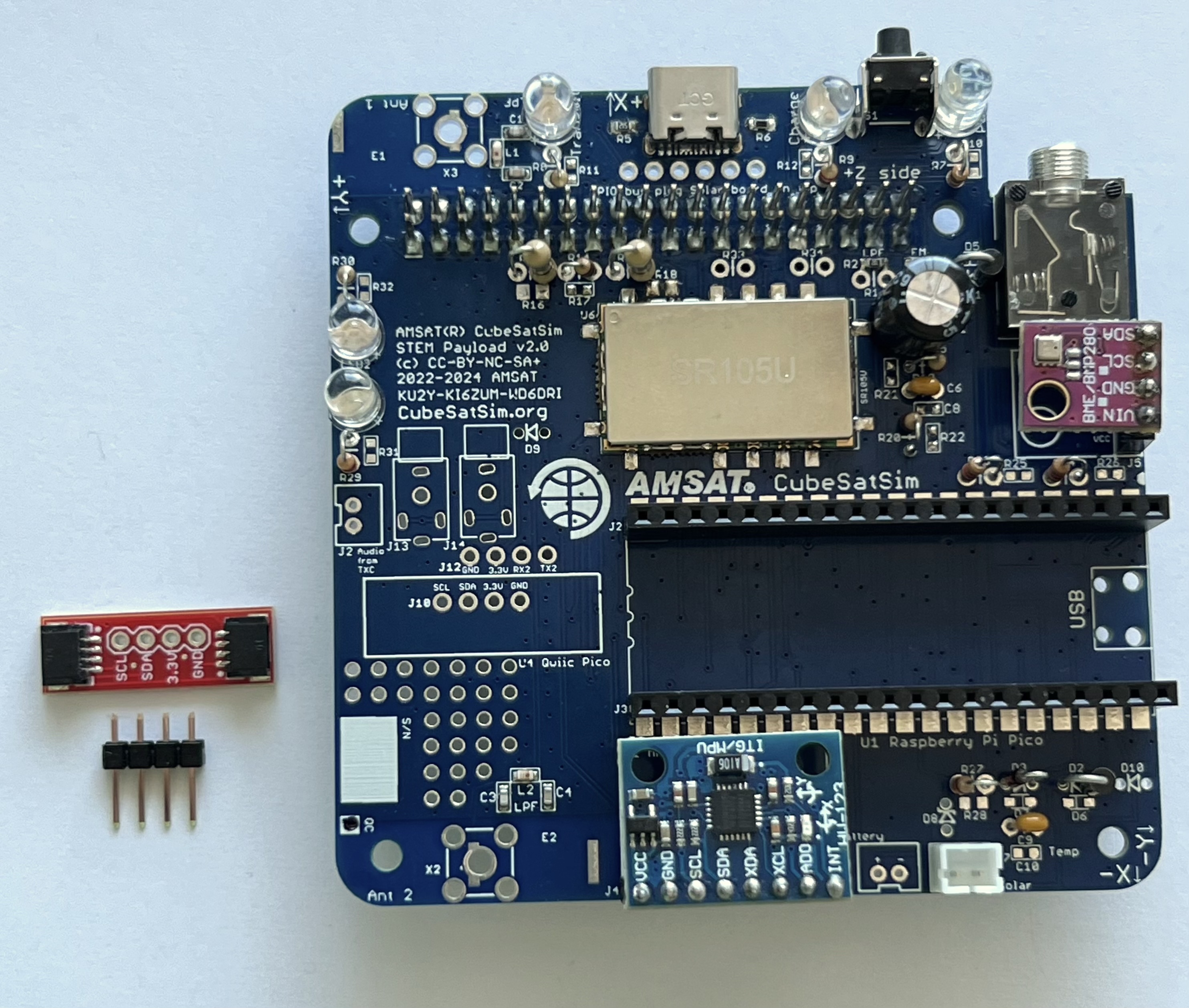
First install and solder the four pin male header J10, long pins down:
Then, install the connector, using blue putty to hold it level:
Next, install the 2.5mm jack J13.
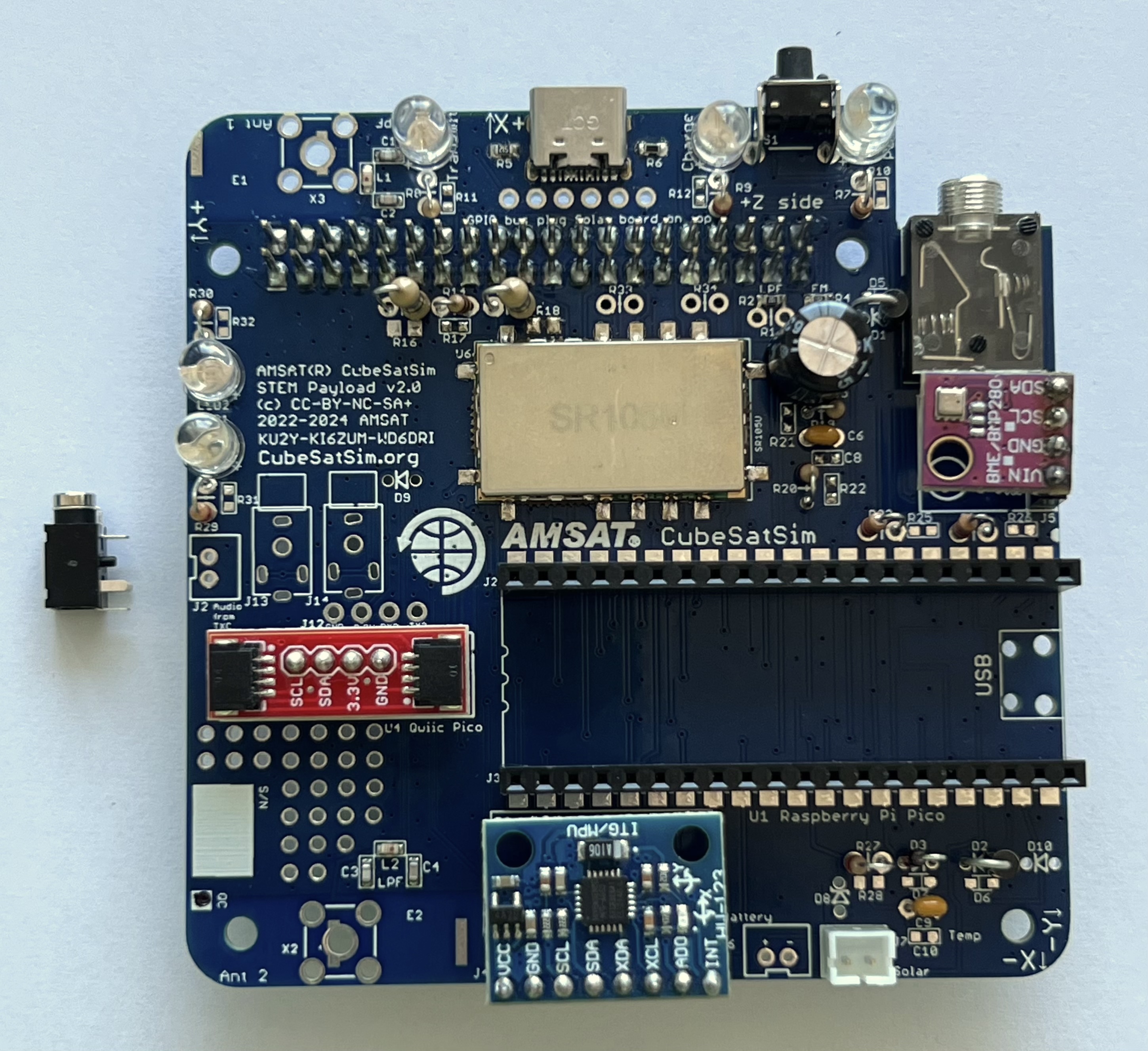
Solder it in place:
If you have an older PCB version and don't have a hack J13, you can still add a 3.5mm connector on the Main Board.
Now, insert the Pico and Pi Zero 2, and you are now ready to test the board.

4.3 Antenna Install
You have a choice of antenna. You can build a SMA antenna (left), a tape measure dipole (center), or two tape measure monopoles (right) as shown here:
SMA Antennas
To connect antennas using SMA connectors, you just need to solder two SMA connectors onto the Main board.
This part takes a lot of heat, so make sure your iron is set to high heat. You might also want to apply liquid flux to the pins to help solder it.
Which gives this:
You will connect SMA coax cable and a rubber duck antenna to each SMA connector when you put the frame together.
Tape Measure Dipole Antenna
Alternatively, you can make a tape measure dipole or monopole (vertical) using these parts:
-
1/4" Tape measure (3/8" and larger ones work too)
-
Two metal M2.5 screws (nylon will not make electrical contact)
-
Two M2.5 nuts, nylon or metal since it is just a spacer to keep the tape measure from touching the PCB.
Extend all the tape out of the measure before cutting or the remaining tape will retract inside and you will need to break open the case. Be careful of sharp edges, and put electrical tape over the cut edges immediately.
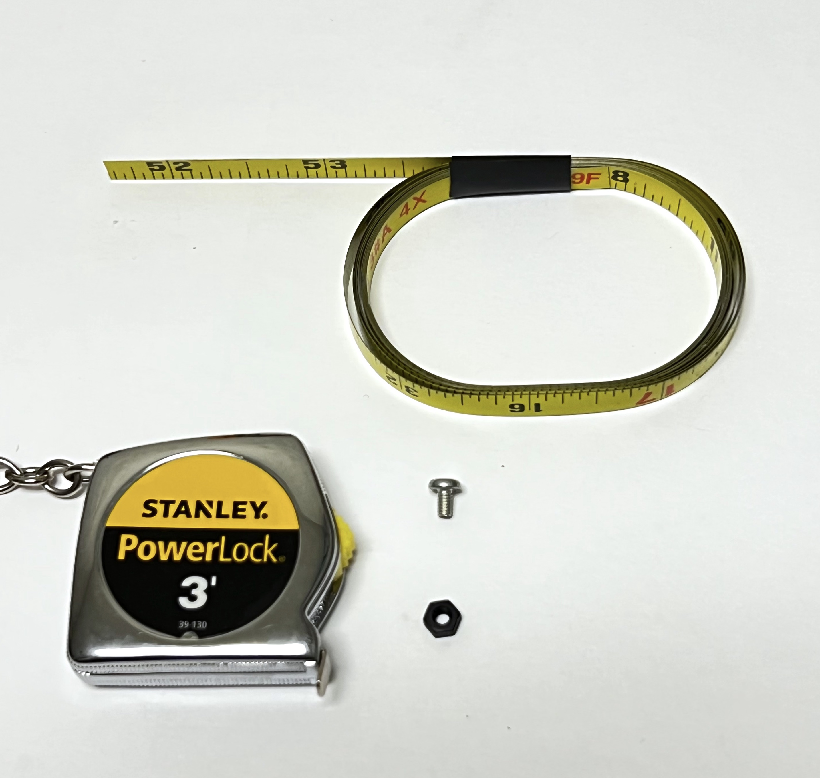
For the dipole antenna, you will need two 1/4 wavelength lengths of tape measure, each with a hole drilled in it. Drilling the hole can be tricky, so drill the hole first, then cut the tape to length. Also, using a punch or small screwdriver to dent the tape in the middle can help prevent the drill from moving around. Also, start with the smallest drill bit you have, ending up with a 3/32" drill bit. It doesn't matter if the hole is slightly off center. Using sand paper or emery cloth, remove the paint from the tape around the hole on the bottom (no numbers) side of the tape measure. Cut to length after you have successfully made the holes, approximately 6.5 inches:
Put the screw through the hole in one of the tape lengths. Then screw the nut onto the screw but don't tighten it all the way.
Press down with the screwdriver as you screw the screw into the PCB and the screw will cut threads into the center hole of the antenna connector as shown. It can be easier to start the screw in the hole without the tape measure at first to begin cutting the threads.
The two tape measure antennas will go through the gap between the solar panels in the frame.
Tape Measure Monopole Antenna
To build the monopole, you need to cut two lengths of tape measure to the same length as the dipole, approximately 6.5 inches long. You need to bend the tape measure next to the hole to a right angle, but don't fold it as it will break off
Screw the screw into the board so the monopole antenna goes vertical. There will be a slot in the top frame piece for the tape measure antennas to stick out.
4.4 Testing
Video
Here is a video of testing the Main Board.
Payload Sensor Testing
You can now test that the Raspberry Pi Pico can communicate with the two sensor boards. Your Raspberry Pi Pico should already have the software installed from Step 2. If not, go back to Step 2 and install the software.
Plug the Pico into the Main board, making sure the micro USB connector is to the edge of the PCB. If the Pico is programmed and functioning correctly, the small green built-in LED should blink once every second.
Connect a micro USB to the Pico and to your computer which has the Arduino IDE installed.

In the Arduino software, open the Serial Monitor by clicking on the magnifier icon in the top right of the window. In the Serial Monitor window, make sure 115200 baud is set in the lower right. You should see a response displayed similar to this:
OK BME280 24.89 1003.96 77.61 21.13 MPU6050 -0.85 -2.48 -1.09 0.19 -0.15 1.02 XS 0 0 0.00
The OK is the status response. The four numbers after the BME280 are the temperature in Celsius, pressure in hPa, altitude in meters, and humidity in percentage read from the purple BME280 sensor. The six numbers after the MPU6050 are the X, Y, and Z axis angular rotation in degrees per second and the X, Y, and Z axis acceleration in g. If you get a series of zeros after a sensor, it means it was not successfully read by the Pro Micro. The three numbers after XS are extension sensor fields that you can set in the code by setting the Sensor1, Sensor2, and Sensor 3 variables.
If you get all zeros for a sensor, you need to determine if it is a hardware or software problem. Running an I2C bus scanner program will tell you if the sensor can be accessed on the I2C bus.
The blue MPU6050 should be at address 0x68 while the purple BME280 should be at address 0x76. If neither device is present on the I2C bus, make sure resistors R1 and R2 are soldered in and are 4.7k in value. If one sensor shows up but not the other, it might be due to soldering on the sensor pins or due to a bad sensor board.
If both sensors show up on the I2C bus but you get zeros in the Serial Monitor, this indicate a software problem.
Gyro Calibration
While at rest (not moving or rotating), the three gyro rotation readings should be close to zero (in the range of -0.2 to 0.2). These are the first three numbers after MPU6050, shown in the red box below. If they aren't, the gyro needs calibration.
With the micro USB cable connected to the Pico and to your computer which has the Arduino IDE installed, open the Serial Monitor by clicking on the magnifier icon in the top right of the window. In the Serial Monitor window, make sure 115200 baud is set in the lower right. In the text box at the top, type the letter c and then click Send to do the calibration. You will see a series of messages scroll by:


Now the gyro rotation readings will be close to zero, as shown in the red box.
Complete Payload Test
When the Pi Zero 2 is plugged into the Main board, the Pi will read the sensor data over the UART and report the data in telemetry. Connect the USB-C power cable into the Main Board and remove the RBF plug to power it up.
(TBD photo showing Pi Zero 2 plugged into the bottom of the Main board powered through the USB-C cable)
When the CubeSatSim software is running, you should see the built-in LED on the Pico blink once, then twice, then repeat.
In APRS (AFSK 1200) mode, the sensor string will be added to the end of the data.
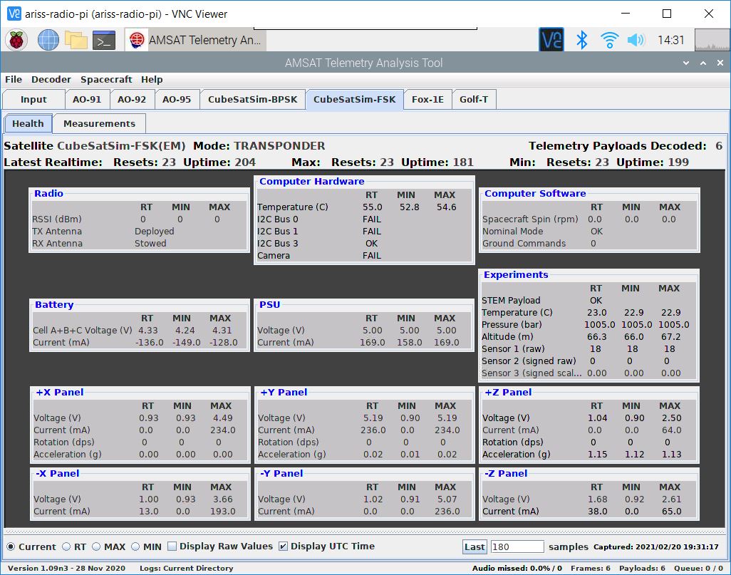
In FoxTelem, in DUV/FSK mode, under the CubeSatSim-FSK tab Health tab, Experiment box, you should see STEM Payload OK and numbers for the other fields. In addition, the rotation and acceleration will also be displayed under the +X, +Y, and +Z boxes.
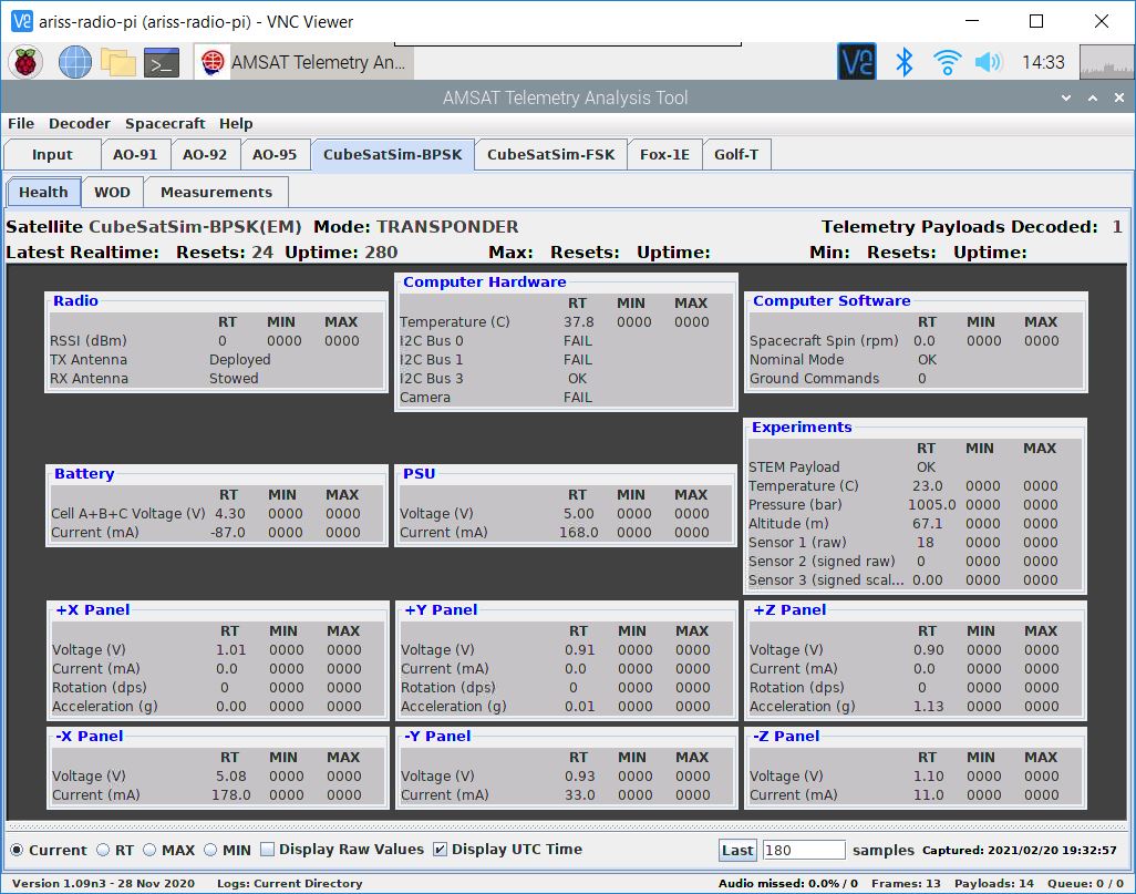
Using the pushbutton, you can switch the CubeSatSim to BPSK mode by pressing and holding the push button until it blinks rapidly three times. Then, if you run FoxTelem in BPSK mode, you can look under the CubeSatSim-BPSK tab and see:
On the spinning turntable, you should see 7-10 degrees per second of rotation and the yellow LED1 on the STEM Payload board illuminated. If the CubeSatSim is accelerated greater than 1.2g, the white LED2 will illuminate on the STEM Payload board.
Payload Serial Connection Troubleshooting
If you see the right output in the Serial Monitor in the Arduino IDE, but you don't see the payload data in the APRS packet or FoxTelem says STEM Payload FAIL, here are some things you can check.
Login to your Pi and type these commands:
cd
CubeSatSim/log | grep ayload
The use of ayload instead of payload will give you the log entries for Payload and payload.
You can also send commands over the serial port like you did with the Arduino IDE using these commands:
sudo apt-get install -y minicom
sudo systemctl stop cubesatsim
minicom -b 115200 -o -D /dev/serial0
Now you should see the same output you saw in the Arduino Serial Monitor.
To exit, you have to type Control-A then z then x then hit Return.
Adding Additional Sensors
Here's how to add more sensors to your Main board.
Additional Sensor Info
The BME-280 Temperature Humidity Barometric Pressure Sensor (small purple board):
https://lastminuteengineers.com/bme280-arduino-tutorial/
Here is some code that displays all the values:
https://github.com/alanbjohnston/CubeSatSim/tree/master/stempayload/bme280test
The MPU-6050 (GY-521) 3-Axis Accelerometer and Gyro (larger blue board with red or green LED):
Here is some code that displays all the values:
https://github.com/alanbjohnston/CubeSatSim/tree/master/stempayload/GetAllData
The next step is to build the Battery board.