1. Main Board 1 - alanbjohnston/CubeSatSim GitHub Wiki
If the images on this page fail to load, you can download a PDF of the page here.
1. CubeSatSim Main Board Assembly Part 1
In these steps, you will start building your Main Board.
These steps are used to build a v2.1 CubeSatSim shown here:

To do this, you will need the parts in the BOM and these tools:
- Safety glasses (to protect eyes while soldering or trimming leads)
- Soldering iron and solder (I use lead-free solder, but leaded solder is easier to work with)
- Needle nose pliers (to bend leads and hold parts)
- Side cutters (to trim leads)
Other tools that are helpful:
- Blue mounting putty (to hold components in place while soldering)
Video
Here is a video showing this assembly step.
Checklist
Here is the Bill of Materials (BOM): https://CubeSatSim.org/bom This board is the first set of parts labeled "Main Board"
The BOM has a sheet "By Steps" which lists the parts needed for each step in order. If you have a Google account, you can make a copy of this spreadsheet ("File" then "Make a Copy") and check off each part as you install it.
For example, here is the checklist for this step:

Main Board Instructions
If you don't have the ability to do SMT soldering, you can instead use an external Band-Pass Filter with SMA connectors. For example, this BPF works quite well https://www.amazon.com/gp/product/B07R8Y1PM4/. For the USB-C connector J9, you can use J8, the Sparkfun USB-C breakout https://www.sparkfun.com/products/15100. And instead of the 1k SMD resistor R2, you can install a through hole 1k resistor in R1.
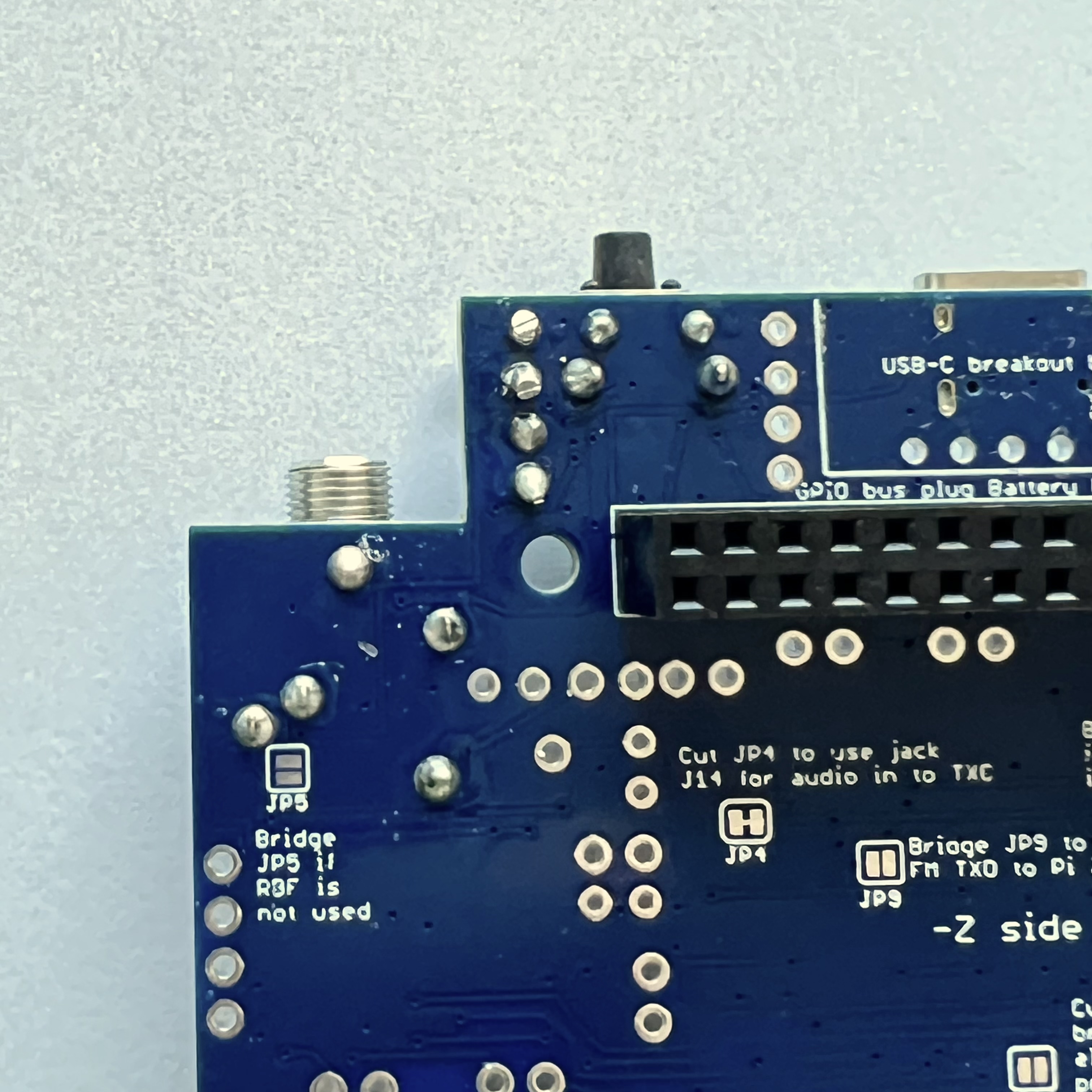
Here is the PCB with the SMT components installed:

If you aren't good with SMT soldering, you can make a board with just the Low Pass Filters and the FM Transceiver module as SMT, with the USB-C and other components as through-hole soldering. Here are the steps to install the SMT components. (The SMT parts are in the BOM in the SMT Parts tab).
Here's the v2.1 PCB:


Schematic
Here's the schematic for the v2.1 Main board for reference:
Assembly
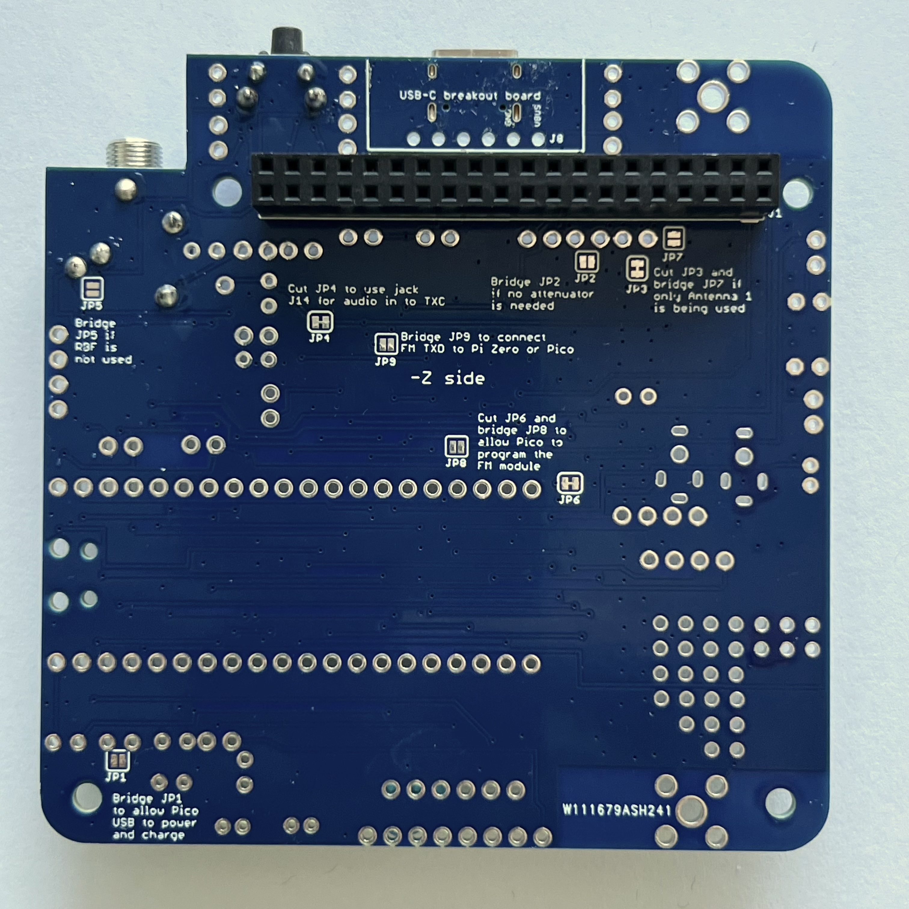
The printed outlines on the board indicate that a part should be installed on that side, with the pins soldered on the other side. For components with multiple pins, solder just one pin first, then flip the board over and verify that it is flush with the board and straight. It is a lot easier to fix this with only one pin soldered than with multiple pins. It is also one last check to make sure you are mounting it on the right side. For some parts, such as resistors or diodes, mounting on the wrong side won't matter. For others, such as LEDs and switches and connectors, mounting on the wrong side will make it more difficult to mount the solar panels. But other parts, such as a the stacking GPIO headers or the INA219 boards, must be mounted on the correct side, so double check carefully.
This photo shows the set of parts to be mounted in the next steps on the PCB:

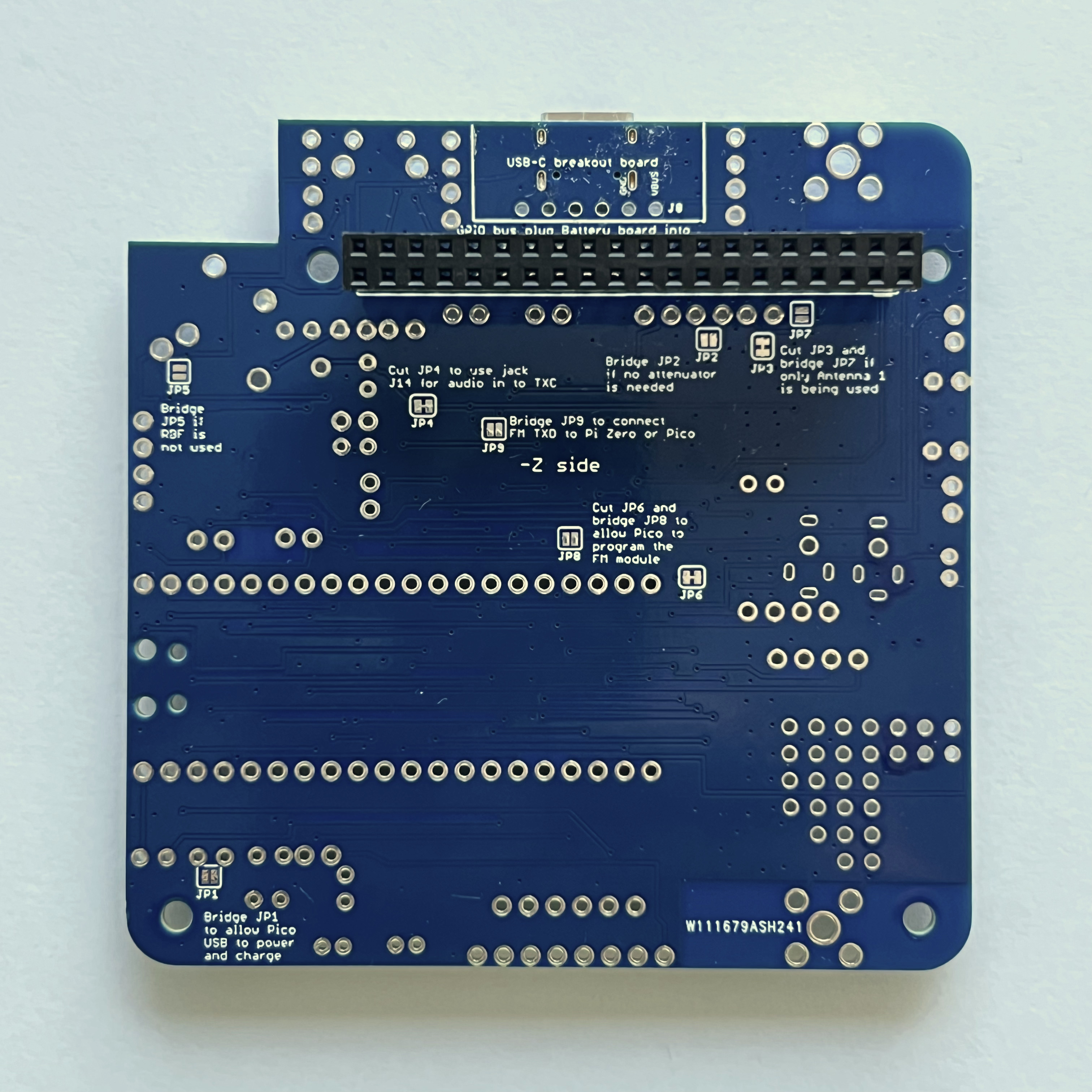
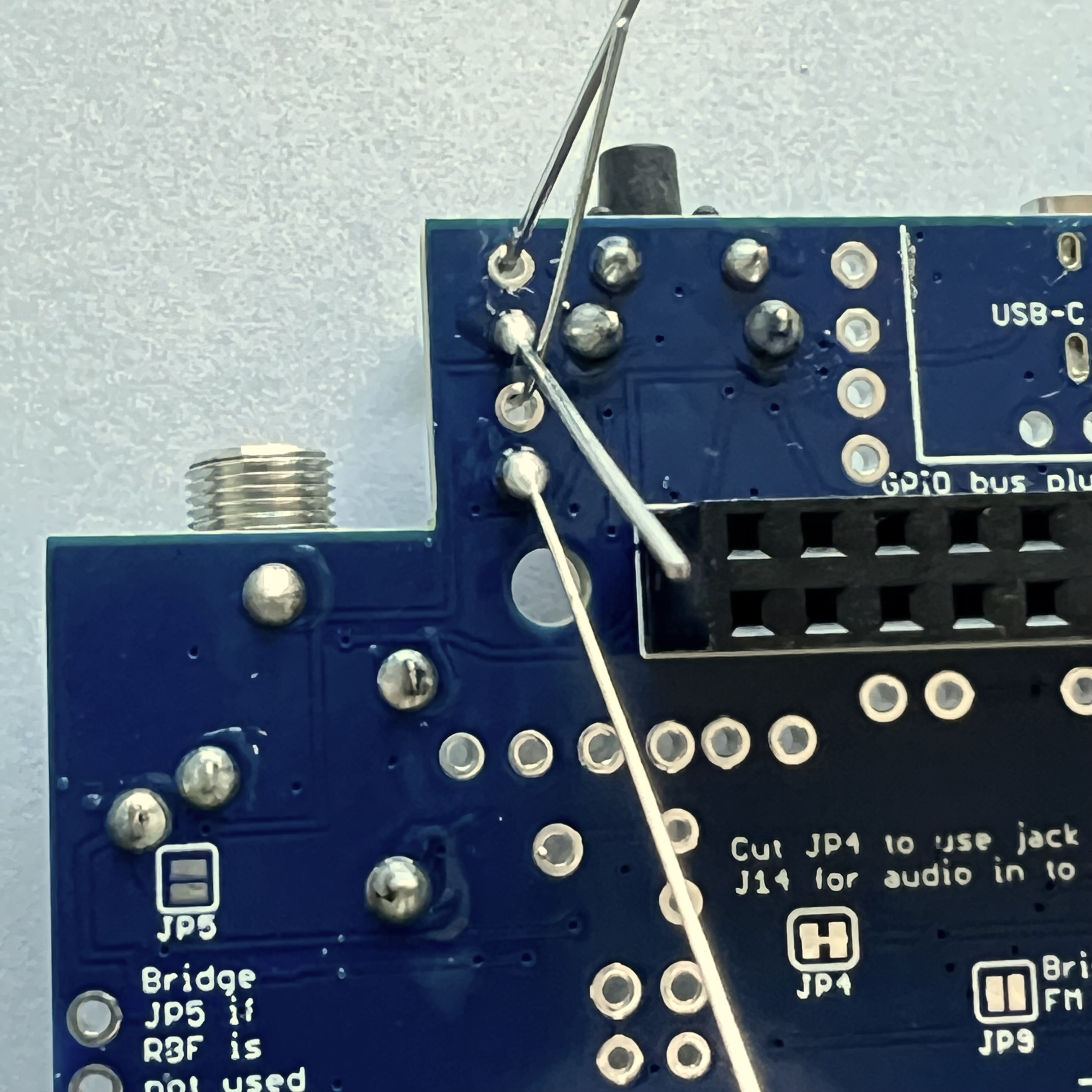
Start with the stacking GPIO header J1. We use the Raspberry Pi GPIO as our spacecraft bus, and it connects the Pi and the three boards together. We will insert the stacking GPIO header on the bottom of the PCB and solder the pins on the top of the PCB.
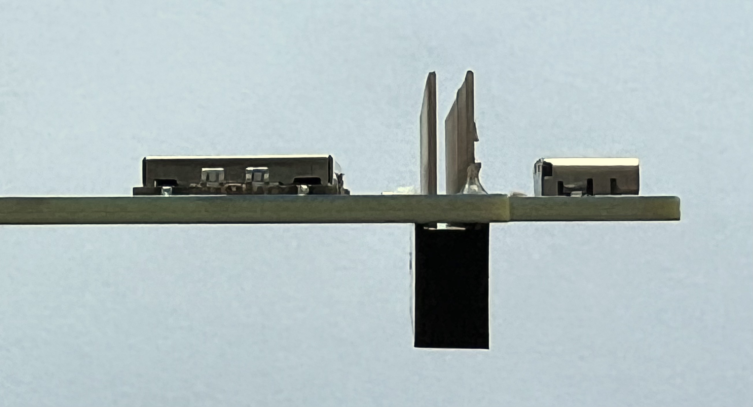
IMPORTANT: Do not trim the leads on this stacking header, since the long leads are needed to plug the next board on top! It is also important that you don't get excess solder on the top of the GPIO pins or it might be hard to plug then next board in.
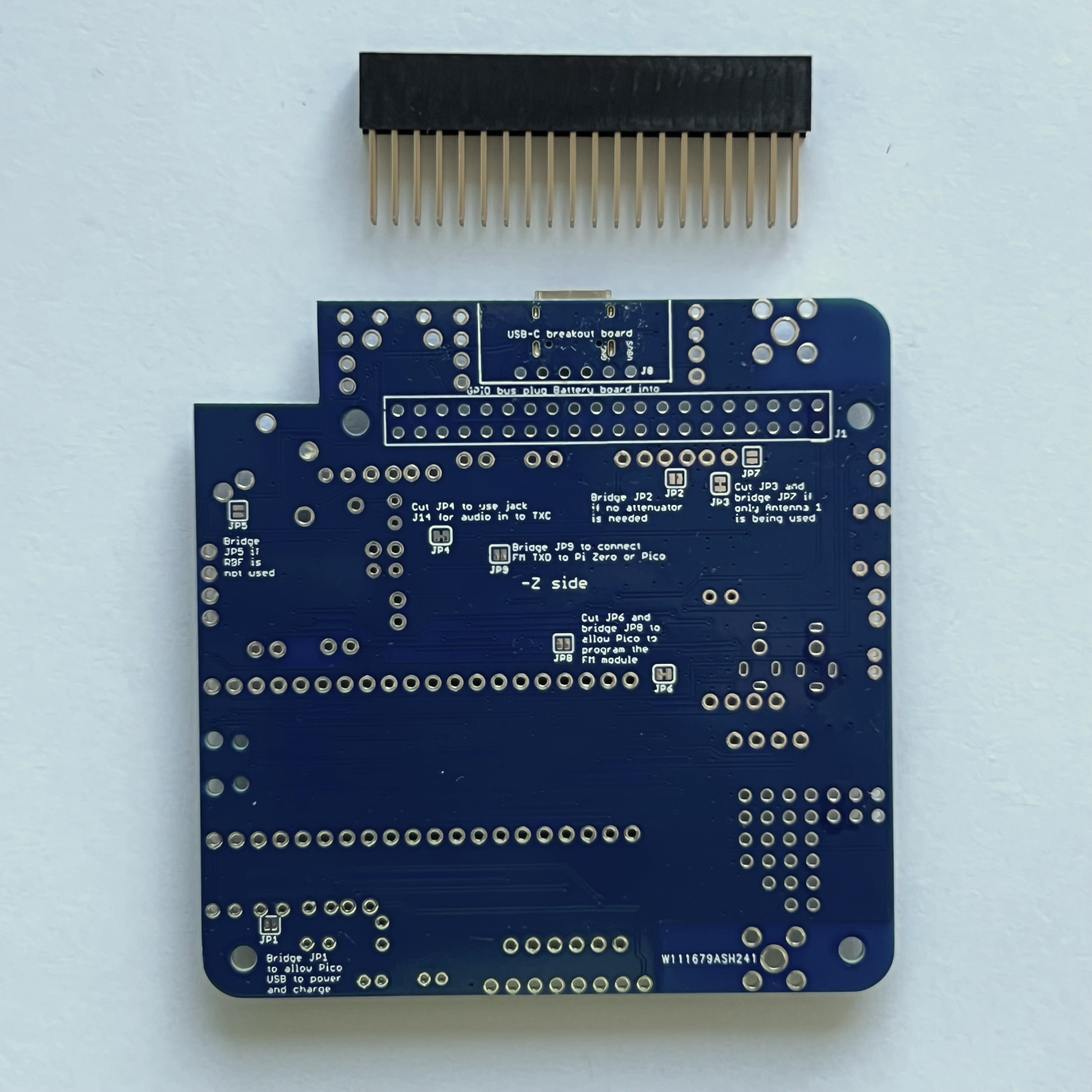
Flip the PCB upside down and insert the GPIO header:
Flip the PCB to the top to get ready for soldering. To make it easier solder, the PCB has enlarged pads making it easier to apply heat.
If you place your soldering iron on this pad touching the pin, you should be able to get heat to both the pin and pad to solder it.

Solder only one pin on the corner of the connector:

Double check that it is pressed down all the way and straight before going back and soldering any other pins:
If everything is good, solder one pin on the other corner and check to make sure it is straight and flush with the PCB. Check the connector again carefully. If it looks good, go ahead and solder one row of pins. Here's how it looks on the top of the PCB with one row soldered in:

Then solder the 2nd row. The solder should fill the pad but not go up the pin or it will be difficult to insert another board into the connector.
The rest of the components are inserted in the top of the PCB and soldered on the bottom of the PCB.
Next is the push button switch S1. This momentary push button switch is used to change modes or shutdown when it is running:

Insert the switch in the top and solder the four leads on the bottom of the PCB:

Here's how it looks up close:

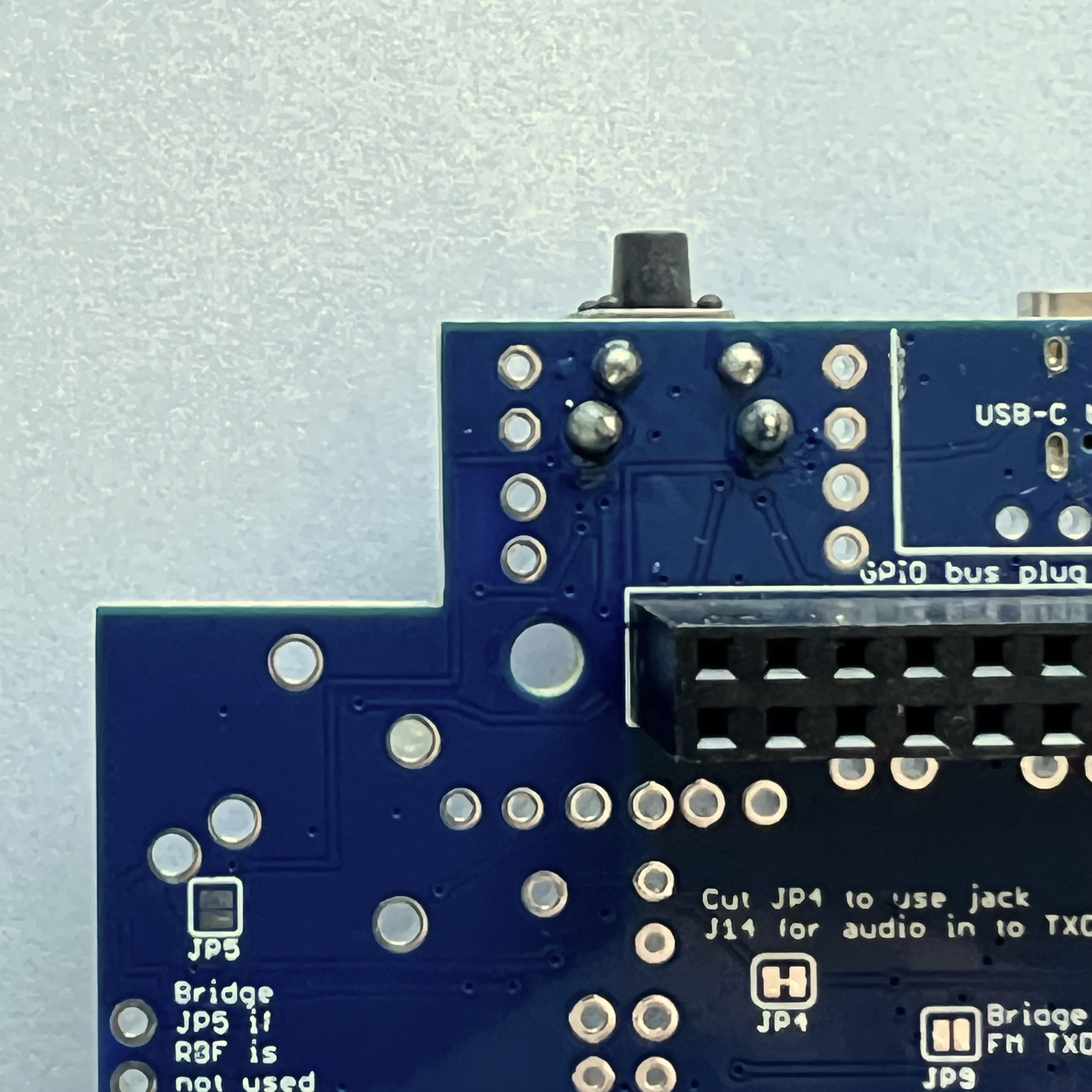
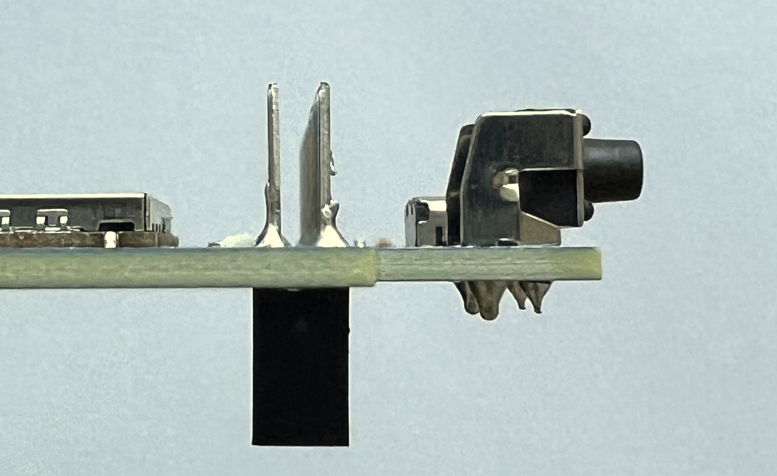
Then, solder X1 the 3.5mm audio jack, which has a contact switch (you can see the contacts with the springs if you look through the clear cover) for our Remove Before Flight (RBF) switch. This switch disconnects power from the CubeSatSim for transporting or storage, or, on a real CubeSat, prior to launch.


Flip the PCB over and solder the 5 leads:
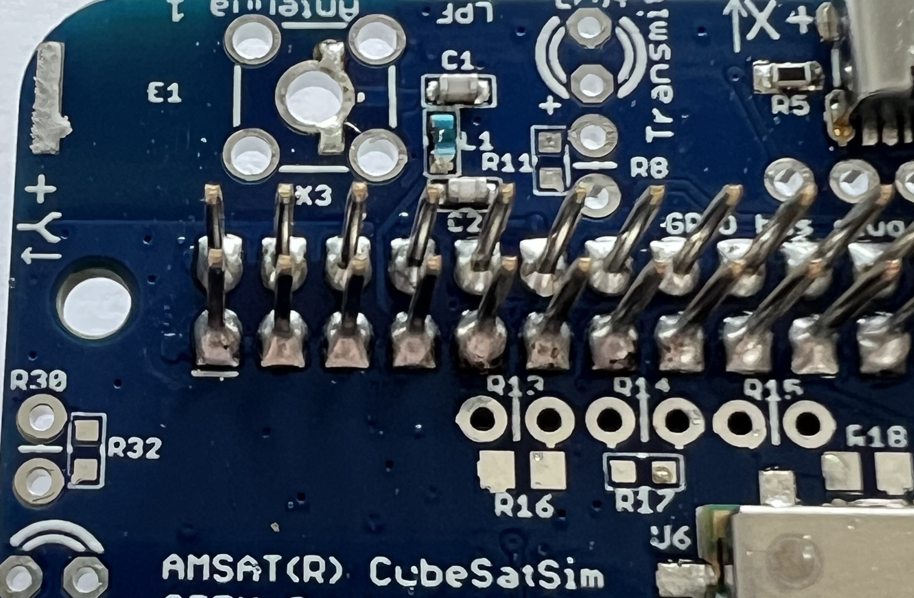
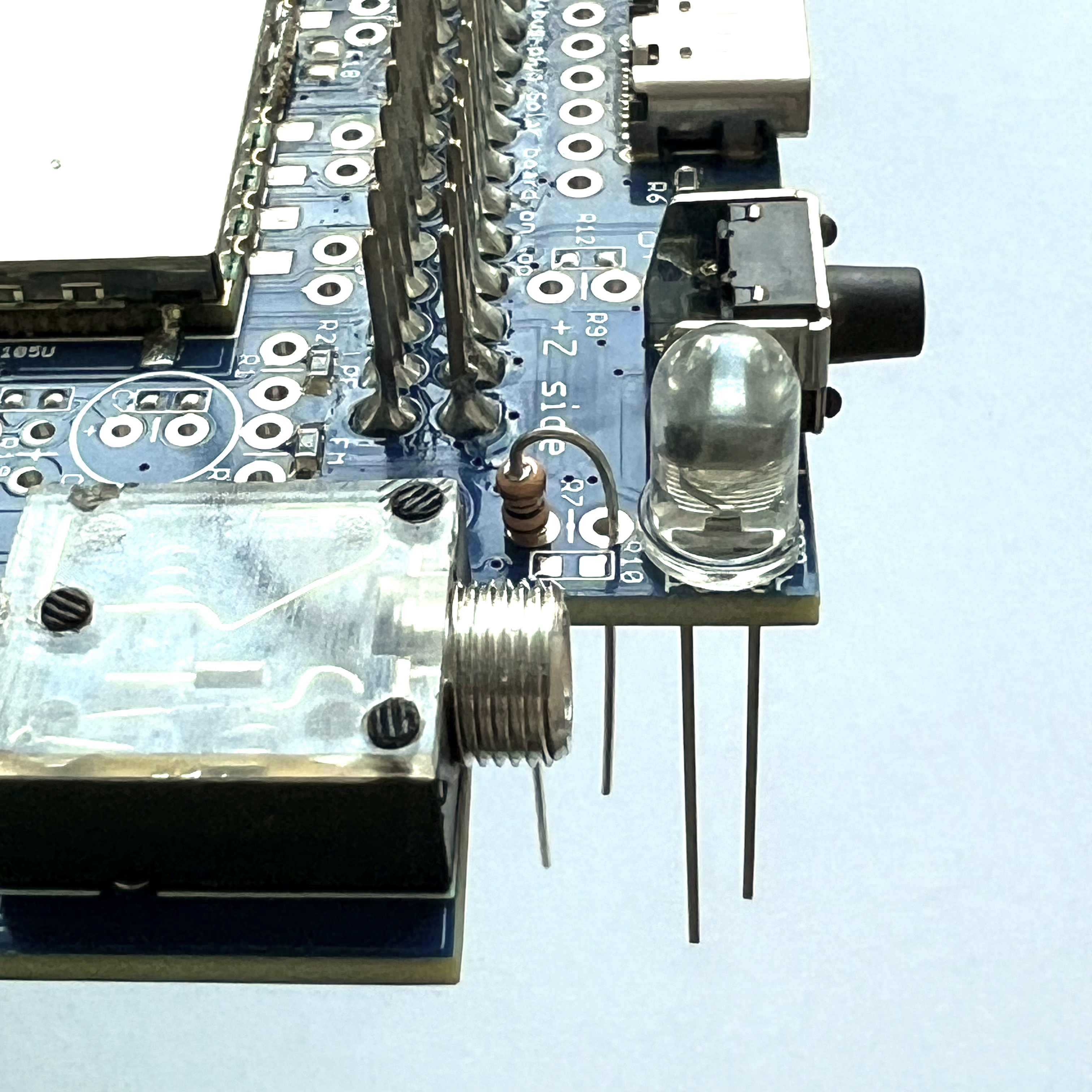
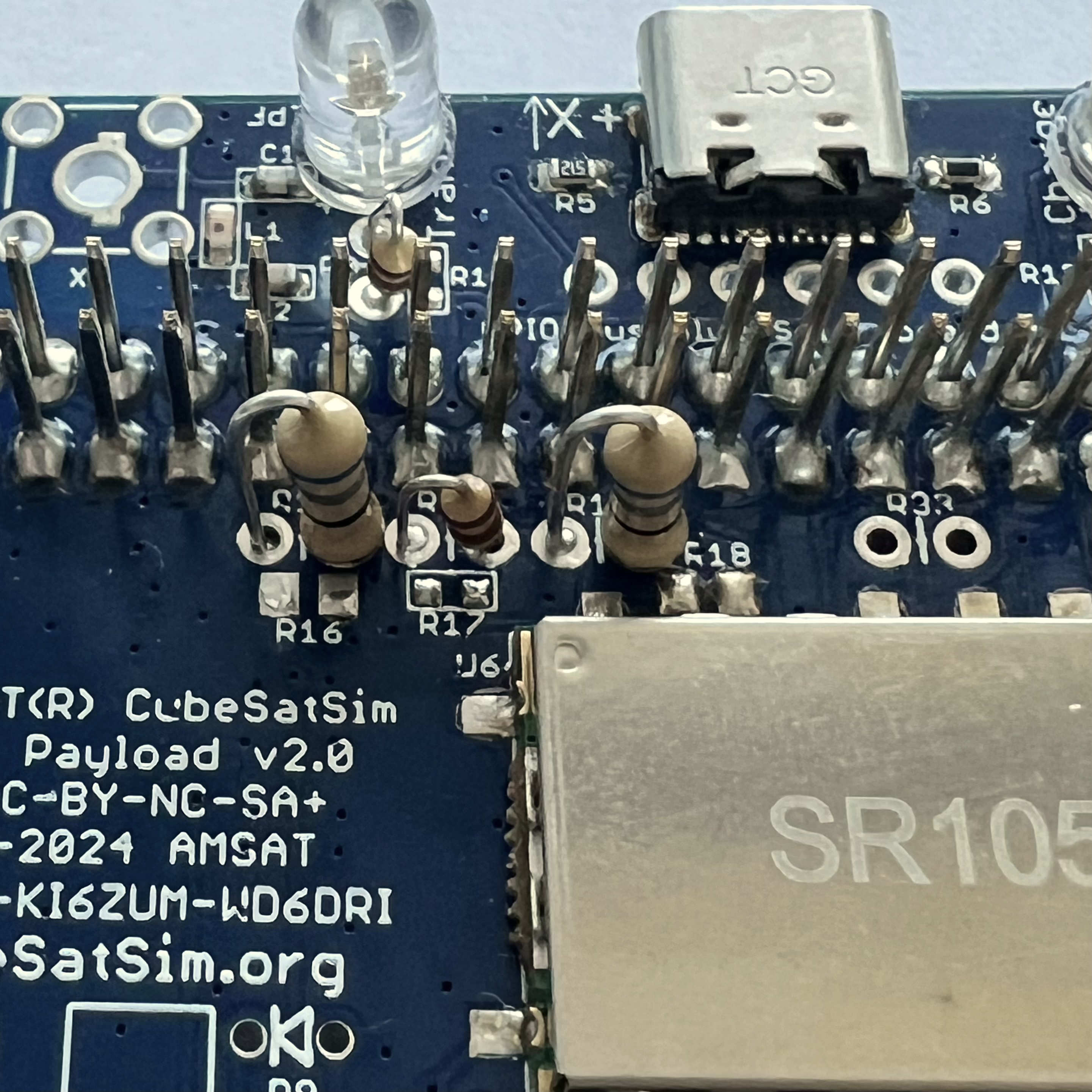
Next we will solder the resistors R7, R8, and R9, and the three LEDs LED3, LED4, and LED5. If you are using clear lens LEDs, be careful not to mix up the colors! If you are not sure, test them with 3.3V and resistor R11 to see what color it is. LEDs need to be installed with the correct polarity (one lead is + polarity and the other lead is - polarity) or it will not illuminate. The longer leg on the LED is the '+' lead and should be away from the edge of the PCB. Also, if you look at the LED lens from the top, it is circular but there is a flat side that marks the '-' side. So the flat side of the LED should be towards the edge of the PCB.
To save space on the PCB, all resistors and diodes are mounted vertically, so you have to bend over one of the leads to get a U-shape, allowing it to be inserted into the two closely-spaced holes. This photo shows the green Power LED3 and 1k Ohm resistor R7 (the color bands on the resistor are brown black red - see https://en.wikipedia.org/wiki/Electronic_color_code for details) which are about to be inserted next to the RBF switch. Note the longer plus lead of the LED is on the bottom here:

Insert the LED and resistor then flip the PCB upside down. Bend the leads slightly so the part is held in place. Solder one pin on each part:
Make sure the parts are straight and inserted all the way into the PCB:

Solder the other pins, then trim the excess leads with side cutters.
Here's how the resistor and LED leads look after they have been soldered on the bottom of the PCB and the excess leads trimmed:
Next, install the red Charge LED5 and 220 Ohm resistor R9 (color bands red red brown),

Then install the blue Transmit LED4 and 100 Ohm resistor R8 (color bands brown black brown):

Next install the diodes D1 and the PTC F1. If you have the Main v2.0 board which does not have F1 marked, see the note below.
Diodes have polarity marked with a band on one side. In this photo, the white band on the diodes is to the left which matches the symbol markings for D1:

Diodes are mounted vertically like the resistors. Note the band is on the upper side in this photo:

Here's a closeup of the diode and PTC installed:

If the diode is backwards, when we plug in the USB-C power cable, the Red LED will illuminate but the board will not power up!
Note that if you have the Main v2.0 board that has two diodes D1 and D4, you can still install the new diode BYW27-400 as D1 and the PTC as D4 like this:

Next install the two 68 Ohm resistors R13 and R15 (big 1/2 Watt resistors with color bands blue gray black) and the 180 Ohm resistor R14 (color bands brown gray brown) in the attenuator circuit:


We can now test the Red LED using the USB-C connector.

Plug your USB-C cable into a power plug or a computer, then plug it into the USB-C connector on the PCB and the Red LED should illuminate.

If it doesn't, check LED5, resistor R19, and the USB-C connector.
The rest of the LEDs need the Raspberry Pi Zero WH programmed and plugged in, which is our next step!
You have completed Part 1 of building the Main board. Here's how the board looks so far:
Next step is to Install the Software.