fpsoc hardware description project - UviDTE-FPSoC/Zynq7000-dnn-inference GitHub Wiki
A project with a hardware description for ZedBoard has to be created in order to perform inference of any DNN. This page will guide you through the creation of this project step by step. If you don't want to go through all the process, there is a copy of the file you need in order to configure PetaLinux in this link. The essential hardware block, in order to be able to implement DNN onto the ZedBoard, is the DPU (Deep Learning Procesing Unit), which is an IP block created by Xilinx. This IP block can downloaded with the DPU target reference design (TRD) v3.0 here.
An newer version of the block can be downlownloaded in the Xilinx Vitis-AI repository. At the moment of writing this guide, the newes DPU version is v3.2. The reason to be using v3.0 is that the newest version is not compatible with the DNNDK v3.1 package, as the compiler generates a kernel that targets the DPU version 1.4.1, while DNNDK is only compatible with version 1.4.0.
This TRD has been created by Xilinx to use the DPU with the ZCU102 board, which has a Zynq MPSoC UltraScale+ chip. Therefore, the only part that is needed from the downloaded file is the DPU IP block, which is going to be imported into the project created for ZedBoard.
Before starting building you Vivado project, make sure you have correctly installed all the Vivado tools as described in the Software Installation page.
- Create a Vivado Design Suite Project
- Import DPU IP into the project
- Import and Interconnect all necessary IP blocks
- Assign register address for the design
- Generate the bitstream
Open the Vivado tool. One easy way to do this in Ubuntu 18.04 LTS would be to open up a terminal window and type in Vivado. Once the software has booted, follow the isntructions:
- Press the
Create Projectoption.
- Give a name to your project, for example ZedBoard_DPU_2019_2. Select a directory to save the project at. In this, case the directory doesn't have to be saved to any special location.
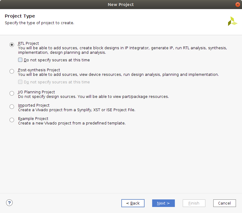
- Select an RTL Project
- Click next in the
Add SourcesandAdd Constraintswindows. - In the
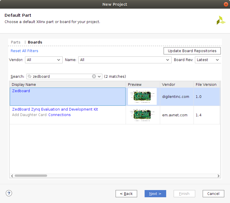
Default Partwindow, select the boards option and look for ZedBoard in the 'Search' menu, as shown in the image. Once you have selected ZedBoard, click next.
- Once you are in the project summary, click
Finish.
The easiest way to proceed would be to download the DPU TRD v3.0, available at the AI Developer site.
Now, within the downloaded archive, enter this directory.
cd <dpu-trd_donwload_directory>/pl/srcs/
In this directory there is a folder named dpu_ip. This is the folder which contains the DPU IP block that is necesary to import into the previously created project. It is not mandatory, but recommended, to copy this folder into the ZedBoard_DPU_2019_2.ip_user_files folder project. Open up a terminal in the directory which is shown above and enter the following commands.
cp dpu_ip /media/arroas/HDD/MinhasCousas/EEI/Mestrado/2_Curso/TFM/vitis-dnn/ZedBoard_DNNs/ZedBoard_DPU_2019_2/ZedBoard_DPU_2019_2.ip_user_files/
It is possible to now go into the Vivado project and press the Tools scroll-down window. Press on the Settings option, which will open a new window.
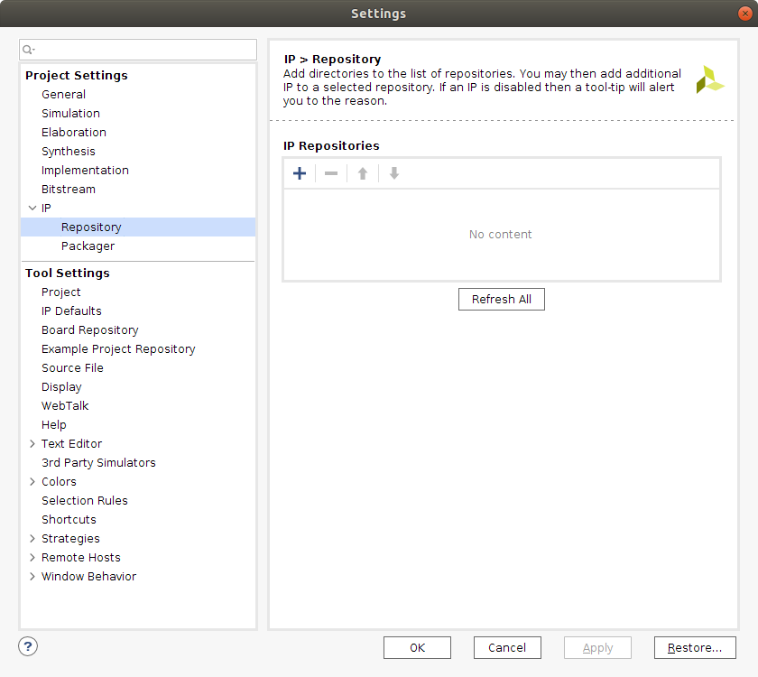
In this window, press the IP >>> Repository option. You can now press the add + option and search for the directory the dpu_ip folder was copied to. After this, press the Select button.
This action will import the DPU IP block into you IP cathalog, allowing you to introduce it into an IP Design.
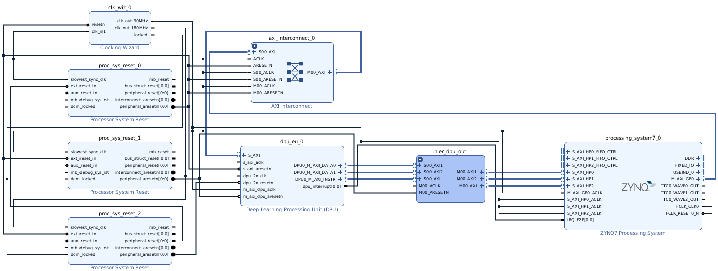
The implementation of DNN inference into the ZedBoard requires a hardware description that contains not just the DPU IP block. In this section, an IP Block Design will be created, including in it all the necessary IP blocks and interconnecting all of them in order to create a hardware description file which will be used to run the DNN inference on ZedBoard.
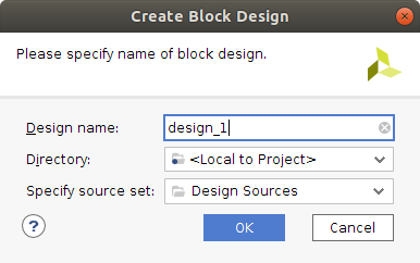
With the Vivado project ZedBoard_DPU_Config opened, go to the Project Manager, at the left side of the Vivado software window and press Create Block Design, under the IP INTEGRATOR option. A new window pops up, which allows giving the block a name, ZedBoard_DPU_HW, and specifying a directory and source set for the design. This options shall be left as default.
The IP Block Design is now created. In order to import a new block, right click in the diagram window and press the Add IP option. This action enables a window where it is possible to type in the name of each of the IP blocks which have to be imported. Include the following ones:
This is the IP block which describes the ZedBoard XC7Z020-1CLG484C Zynq-7000 AP SoC. The configuration of the Processing System (PS) is now described.
First of all, double click the Zynq block that was just imported into the project. Once the Re-costumize window pops up, click on the Presets option and select the ZedBoard preset. The preset will therefore be applied, which will enable the most common periferics of the ZedBoard such as the UART port.
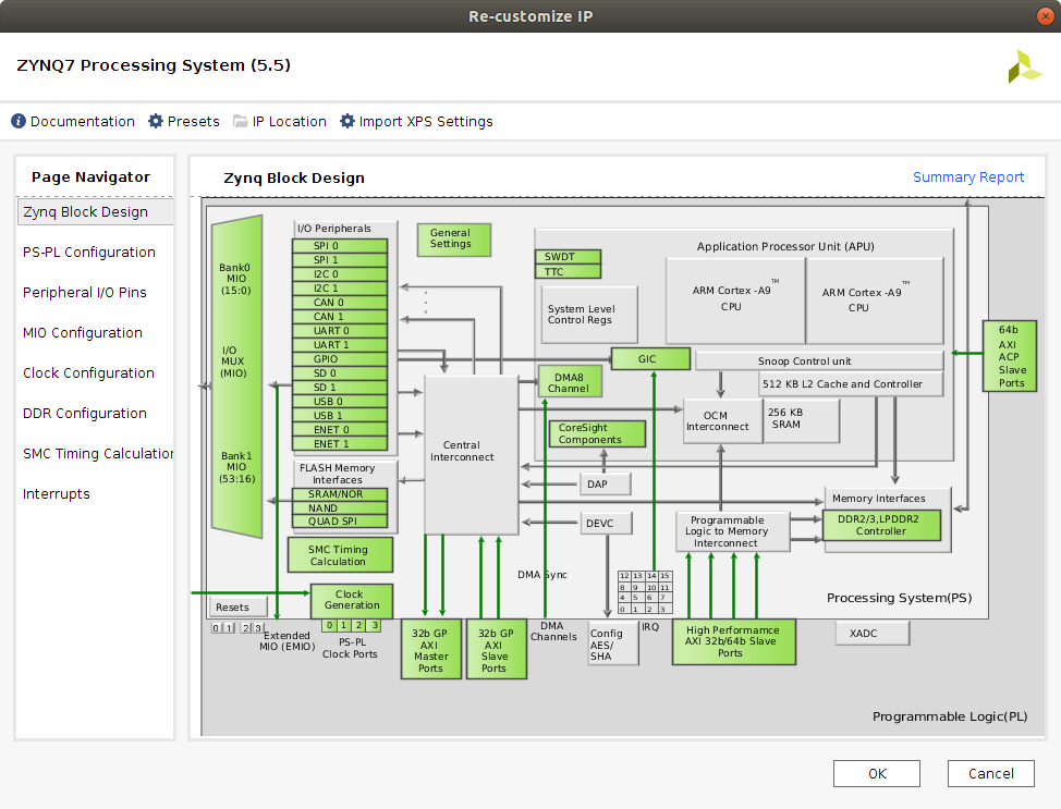
The preset sets up several signals that will be needed later on in the DPU configuration, but we will indicate the process of activating them all.
-
FCLK_CLK0. This signal creates a 100 MHz clock signal needed for the DPU register configuration. This signal is a low frequency signal, as the registers are only configured at the beginning of any DPU task.
-
FCLK_RESET0_N. Reset signal of the generated FCLK_CLK0 clock signal. It is generated automatically when enabling the previous signal. -
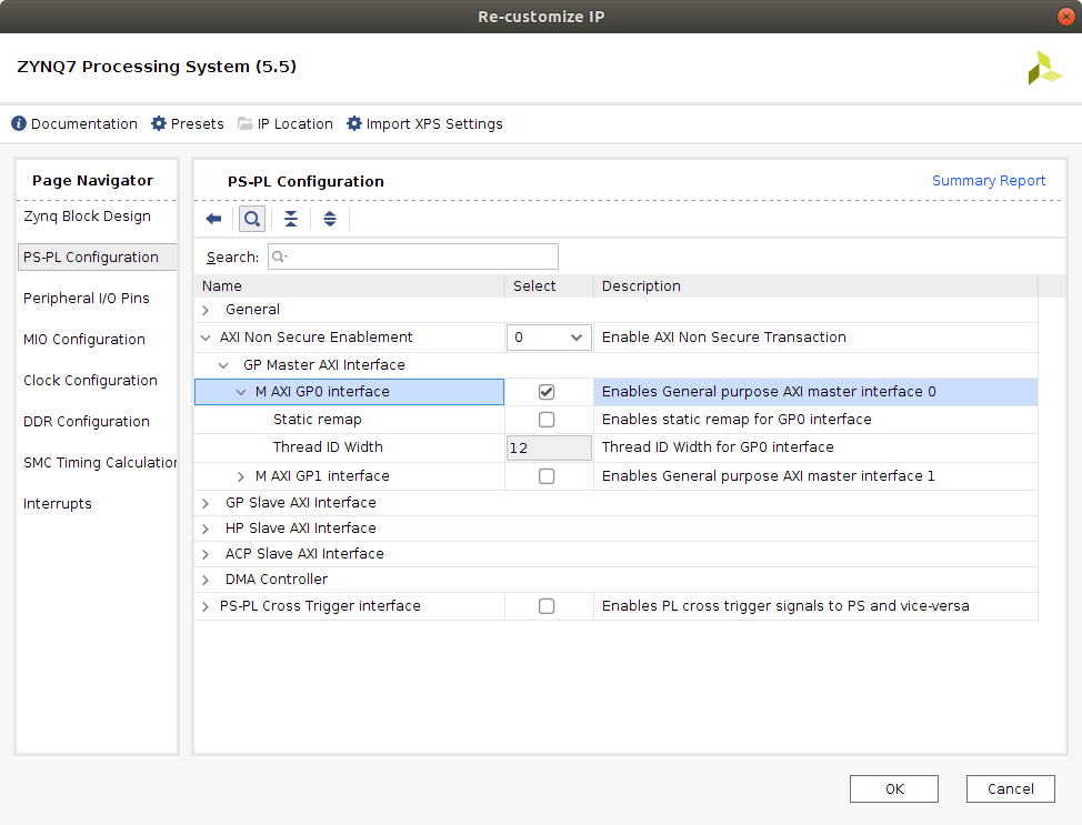
M_AXI_GP0. The PS communicates with the Programmable Logic (PL) through the 32-bit General Purpose AXI interface to the DPU in order to control the configuration registers of the IP block.
-
M_AXI_GP0_ACLK. When selecting the M_AXI_GP0 port, the aclk signal is added as default. This signal has to be connected to a clock signal that generates the frequency at which the DPU registers have to be configured. This rate would be the one created byFCLK_CLK0. -
IRQ_F2P[0:0]. Interrupt input port of the PS which enables the PS to receive the interruptions generated by any core of the DPU.
-
S_AXI_HPx. It is necessary to add three High Performance AXI interfaces to the processor in order to communicate data and instructions with the DPU. The picture shows how to set up three of the four available ports. The data communicating ports have to be 64 bits, and the instruction port can be 32 bits. Boards with 128-bit support for the AXI interface should use this option as the DPU data ports can work with 64 or 128 bits of width. Once these three ports have been added, two signals for each of the ports are created as well.

-
S_AXI_HPx_FIFO_CTRL. Signal that is not going to be used. -
S_AXI_HPx_ACLK. Frequency signal at which the DPU is going to exchange instructions and data with the PS. Has to be connected to the same rate as the data controller clock of the DPU.
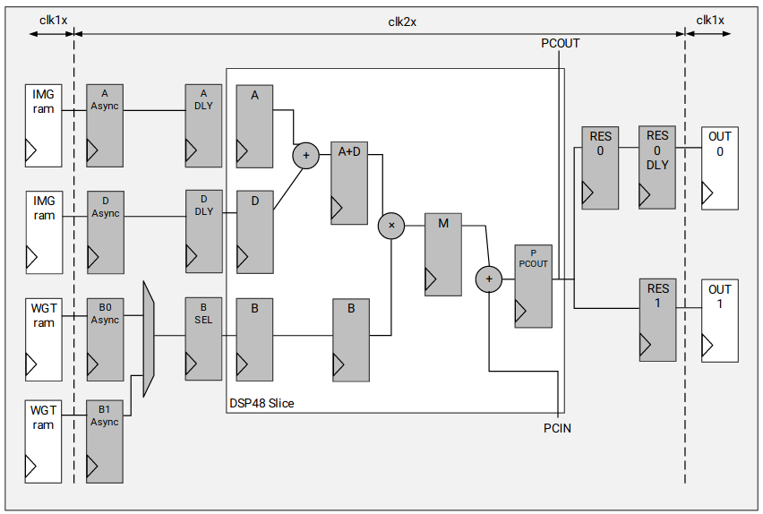
Inference of the DNN on the ZedBoard is going to be executed in the programmable logic of the device through an IP block created by Xilinx, the Deep Learning Processing Unit (DPU) v3.0. This block is a programmable engine optimized for Convolutional Neural Networks. It includes a scheduler module, a hybrid computing array module (which acts as the convolutional engine), an instruction fetch unit module and a global memory pool module, as shown in the figure. The figure has been retrieved from the Xilinx DPU IP Product Guide, page 12.

The DPU fetches instructions from the off-chip memory to control the operation of the computing engine, that consists in a deep pipelined design where the deep learning algorithms are executed. This instructions are generated by the DNNC compiler, which is a tool of the DNNDK package that parses the neural network models to an intermediate representation, which is then optimized in order to generate the DPU instructions. On-chip memory is used to buffer input, output and intermediate data such as the weights, biases and activation bits of the models. The processing elements (PE), which conform the structure of the computing engine, integrate multiplier, adder and accumulator IP blocks, as seen in the figure below. The figure has been retrieved from the Xilinx DPU IP Product Guide, page 13.
The DPU block implements the double data rate (DRR) technique, thus the computational clock can have twice the frequency of the data controller clock, speeding up the execution of the neural network layers.
The ability to configure this block enables variations on the amount of resources it demands, such as digital signal processing slices (dSP) or RAM blocks. There is eight possible types of architectures for the convolution engine, which require more or less resources. Each of them can also implement up to three cores, which can be executed in parallel, improving execution performance. Never the less, the memory bandwidth limit of FPSoC devices might not allow to simultaneously use the cores at their full speed. Hence, the flexibility of the device is increased depending on the size of the CNN an application is created for, enabling the sacrifice of execution time performance in favor of flexibility to implement other tasks or vice-versa. Each DPU architecture can also implement up to 3 cores, increasing even more the amount of resources it needs, which might be key when accelerating large CNNs. The DPU’s layer operation features are:
- Convolution and de-convolution
- Depthwise convolution
- Max pooling
- Average pooling
- ReLU, ReLU6 and Leaky ReLU
- Concat
- Elementwise-sum
- Dilatation
- Reorg
- Fully connected layer
- Softmax
- Batch normalization
- Split
All layer operations that aren’t compatible with the DPU IP would have to be executed in the CPU of the FPSoC device, handling the data transfer between DPU and CPU kernels with the DNNDK API libraries. One of the cases this methodology has to be applied is when implementing a Softmax layer with a Xilinx Zynz-7000 family SoC, as the DPU's softmax utility needs to implement a 128-bit bus for data transfer, width not available by any of the AXI ports of the Zynq-7000 devices.
Regarding the structure of the DPU IP block, the internal representation its variables is performed with 8-bit signed integers. Therefore, the executed models have to be quantized, which consists in modifying its weights, biases and activation bit width 32-bit floating point to 8-bit fixed point. The task can be performed with the DNNDK package, which includes a quantization tool that can be used to compress the models targeted for the DPU.
This IP block uses a specialized instruction set, for which the DNNDK v3.1 package provides easy to use APIs. The combination the DPU and the DNNDK APIs erases the biggest drawback of using a FPSoC device for inference, the time consumed in creating the programmable logic programs, while maintaining the flexibility of the device, as the resources that are not used by the the DPU structure can be destined for any other applications.
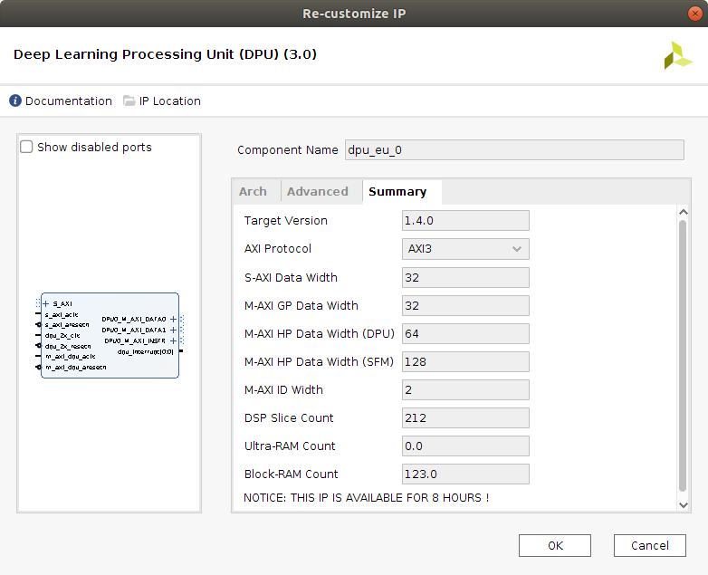
The configuration applied now to the DPU IP block is targeting using the highest amount of available resources, in order to enable the block to perform as good as possible with high computational demanding DNNs. Therefore, the selected architecture is the B1152, with low RAM and high DSP48 usage, as seen in the next two figures. This architecture's peak operations per clock cycle would be 1152 and its theoretical performance for the Z7020 is 230 GOPs.
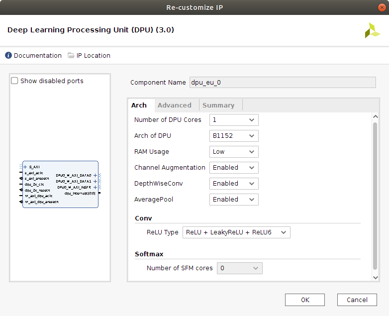
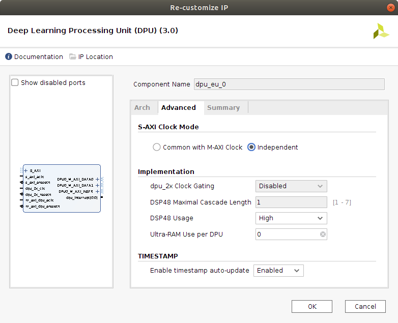
The channel augmentation (increases the efficiency of the DPU when the data input to the DPU doesn't use all the parallel channels of the block), the depthWiseConv layer and the Average Pool layer are also enabled. The depthWiseConv is very important, as it is the main layer implemented by the mobilenetv1 and mobilenetv2 convolutional neural networks, which we run inference on in the Inference of AI Model DNNs with the DNNDK package page. Without this layer, both models cannot be executed. The AveragePool layer enables execution of this layer in DPU rather than CPU, with kernels from 3x3 up to 8x8.
Next figure displays a summary of the features implemented in this project for the DPU IP block.
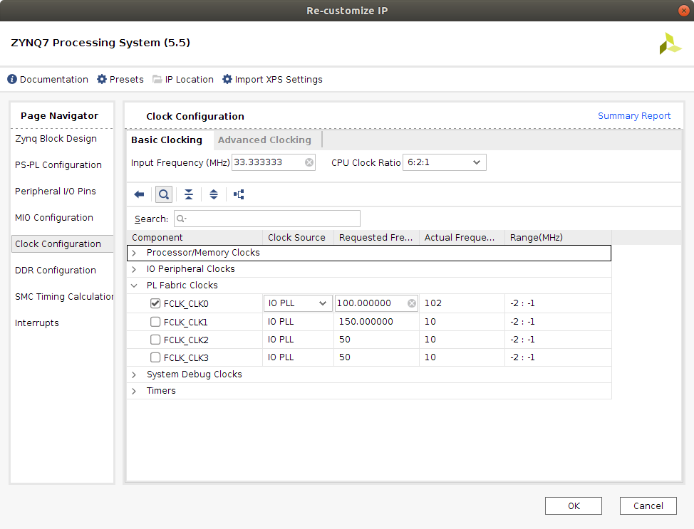
The clock wizard helps creating the circuit for the DPU clock frequencies needed in the design.
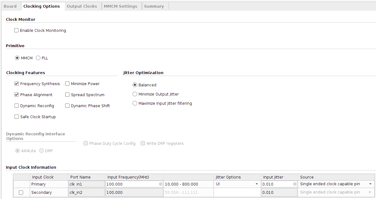
The established DPU configuration works with three different clock rates.
-
Register Clock: this clock is used to for the DPU register configuration before a DPU task is executed. Its rate can usually be lower than that of the other clocks. Xilinx recommends to set it to 100 MHz.
-
Data Controller Clock: with this clock it is possible to control the data transfer between a external memory and the DPU. This is the clock used to send the input data of the DNN that is being executed to the DPU, as well as retrieving the DNN's last layer execution results from the DPU. Depending on the target device the DPU is deployed on, this frequency rate can be different. ZCU102 board can work with a rate up to 325 MHz at least, while a optimal frequency for ZedBoard is 90 MHz.
-
Computational clock: rate at which the DSP blocks are controlled in order to execute the DNN layers of the models. This rate has to be twice as high as the data controller one, due to the use of the DDR technique in the DPU. Its frequency is therefore established to 180 MHz.
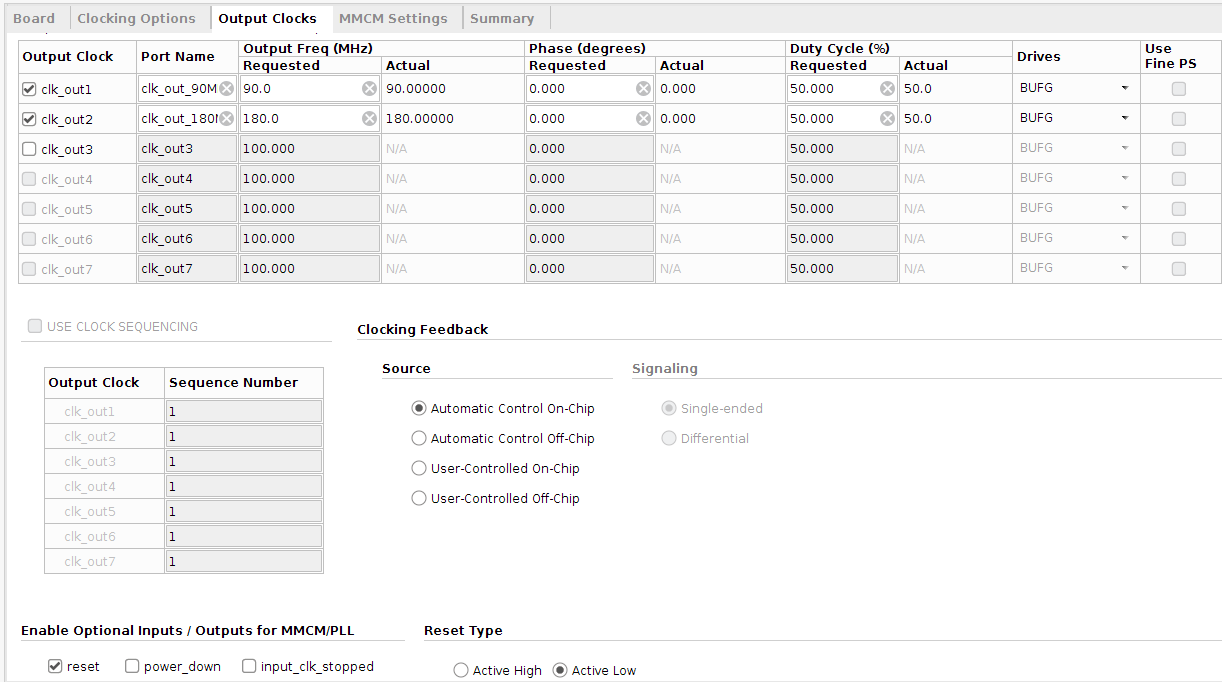
The 100 MHz clock is generated with a PL fabric clock, and the others using a clock wizard with these clock as input.
Each clock rate generated for the DPU needs its own reset, which must be synchronous to the clock it belongs to. Lack of synchronism can create malfunctions in the DPU block. It is recommended to implement the three resets using one Processor System Reset IP block for each.
The AXI Interconnect IP block core allows any mixture of AXI master and slave devices to be connected to it. The DPU IP can be connected to the processing system (PS) with an AXI Interconnection IP as long as the DPU can correctly access the DDR memory space. Generally, when data is transferred through an Interconnect IP, the data transaction delay will increase, reducing DPU execution time performance. Xilinx recommends that each master interface in the DPU is connected to the PS through a direct connection rather than through an AXI Interconnect IP when the AXI slave ports of the PS are enough. When the AXI slave ports of the PS are insufficient for the DPU, an AXI interconnect for connection is unavoidable.
In this case, we have chosen perform the connections using the AXI Interconnect IP, as it is the most commonly used in related works to better handle clock reset activation during data or instruction transfers. In future work it will be considered getting rid of this blocks to see if it has a significant improvement in the execution results of DNNs.
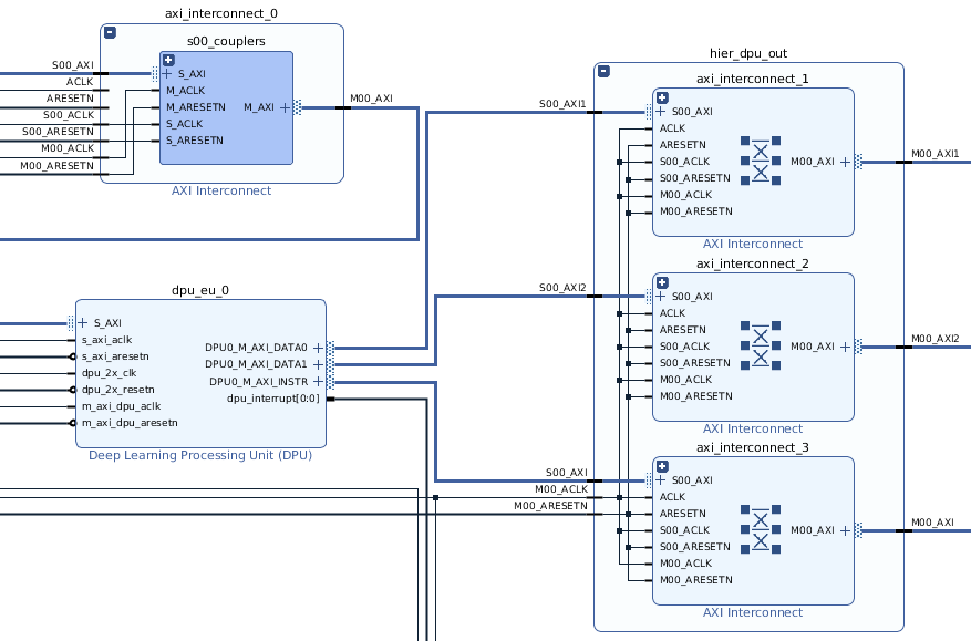
The final block design interconnections is shown in the next figure.
We now mention the connections that have to be taken care the most:
- The DPU AXI slave is connected to the General Purpose interface of the processor through a AXI interconnect block
- DPU data and instruction buses are connected to the High Performance processor AXI interfaces through three AXI interconnect blocks.
- The High Performance bus clock rate of the DPU has to be 90 MHz, the same as the one used for the controller data clock for the DPU
- All the blocks that have any of the clock rates as input should have their reset as input as well, but for the Zynq processor.
The total board resources used by this implementation can be checked in the next figure.
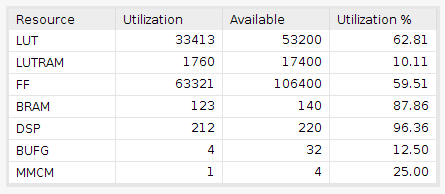
Where:
-
LUT: look-up tables -
LUTRAM: RAM look-up tables -
FF: flip-flops -
BRAM: block RAM -
DSP slice: digital signal processing slice -
BUFG: global clock buffers -
MMCM: mixed mode clock manager
Once all the blocks have been imported and interconnected in the design block, it is necessary to assign an address for the DPU register AXI interface.
Click on the Address Editor window in the project manager, and select auto-assign addresses, which is the option that is right under the Address Editor name.
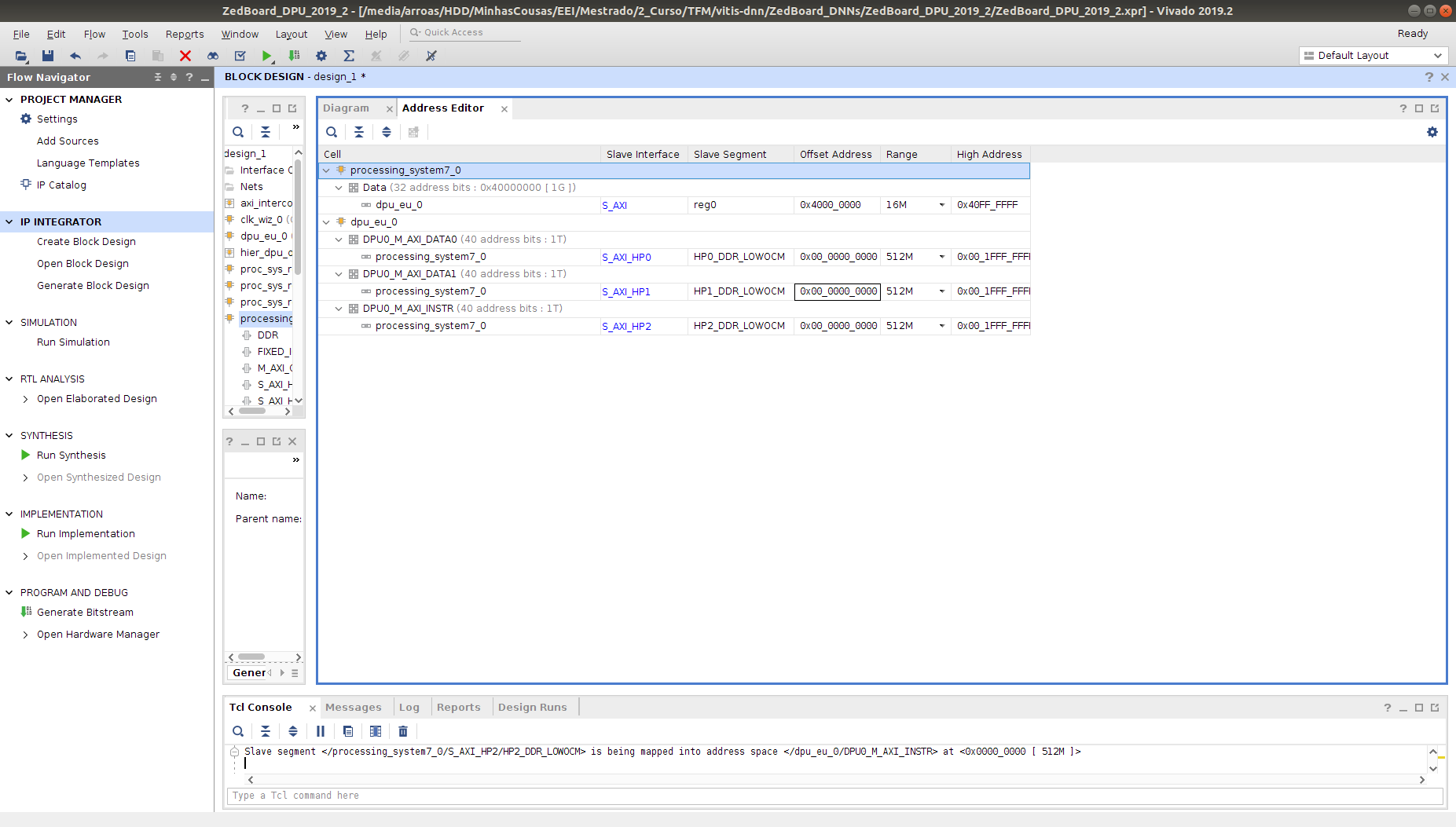
When the addresses have been assigned, it is important to take note of several information in order to, later on, configure the DPU drivers for the DPU. Therefore, check the following data in the Vivado Project:
-
DPU Base Address: The DPU base address can be checked out in the address editor. In this case, the offset address of the DPU is
0x4000_0000, and the high address is0x40FF_FFFF. -
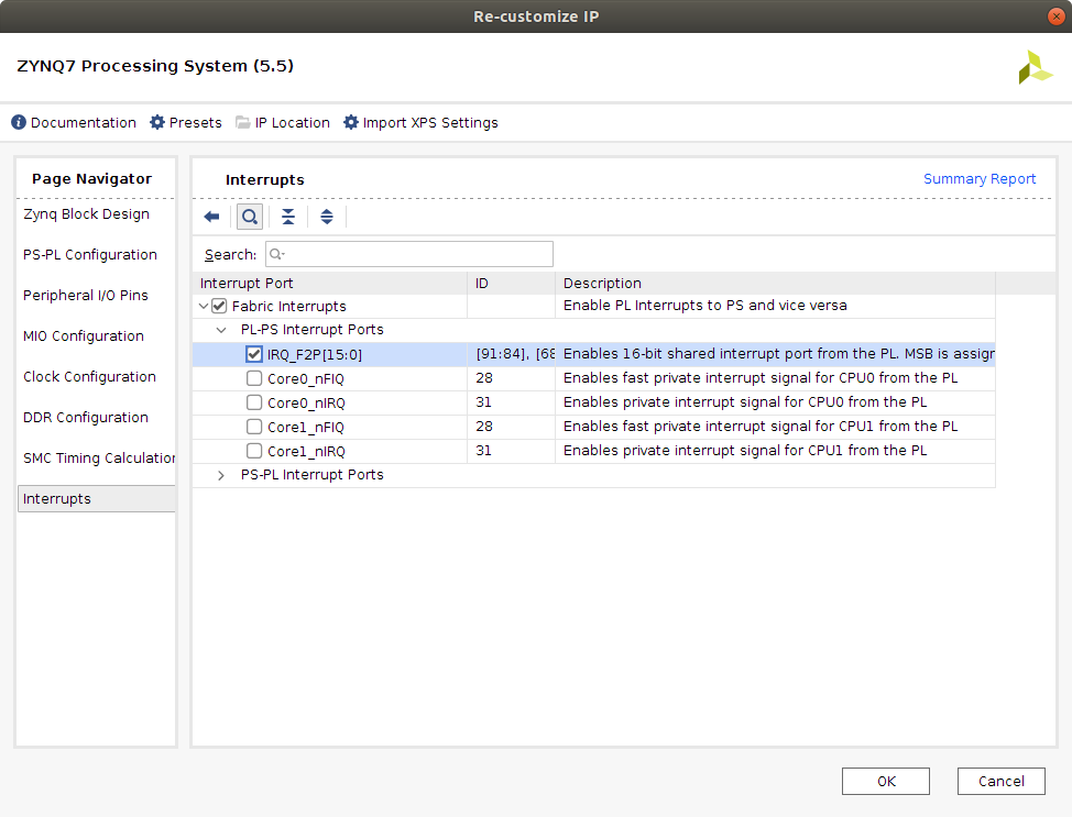
IRQ number: This number is needed for the Linux device tree description. In order to obtain it, it is necessary to obtain the
GIC IRQnumber and subtract 32 from it. The number can be checked in the following image.
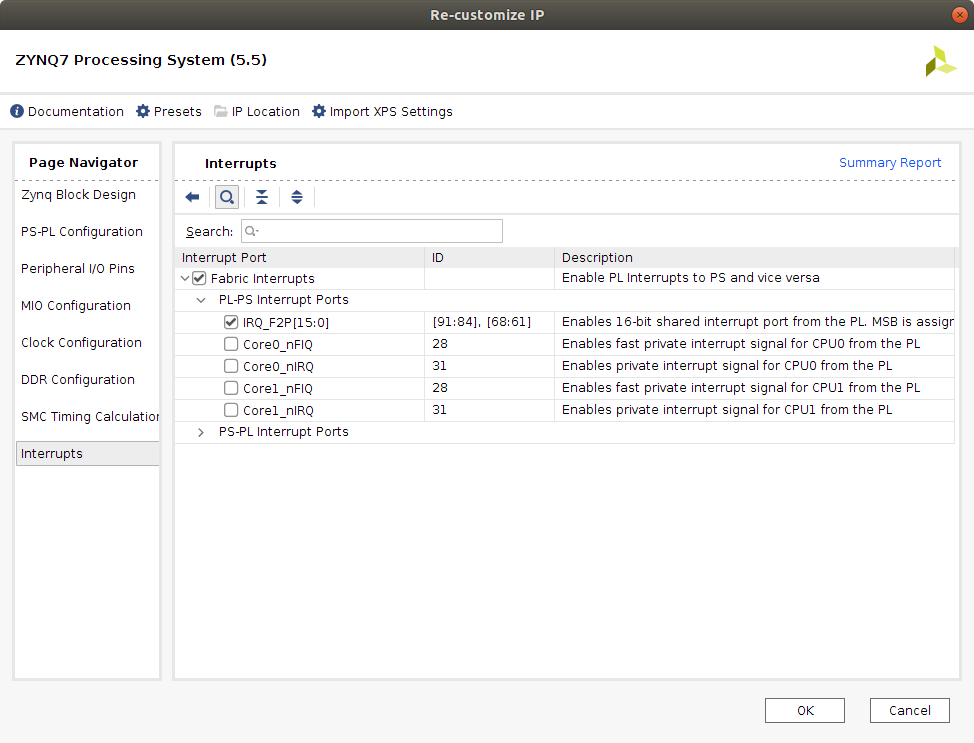
In this image we see that [91:84] and [68:61] correspond to each of the 16 interrupt signals that can be attached to the PS. Therefore, as there is only one interrupt signal for the one core of the DPU, the corresponding signal would be IRQ_F2P[0]. It's GIC IRQ# would therefore be 61. This can be checked out in table 7-4 of the UG585 Zynq-7000 SoC Technical Reference Manual, page 231, which is shown in at the top of the following image. A copy of the document has been uploaded to this repository.
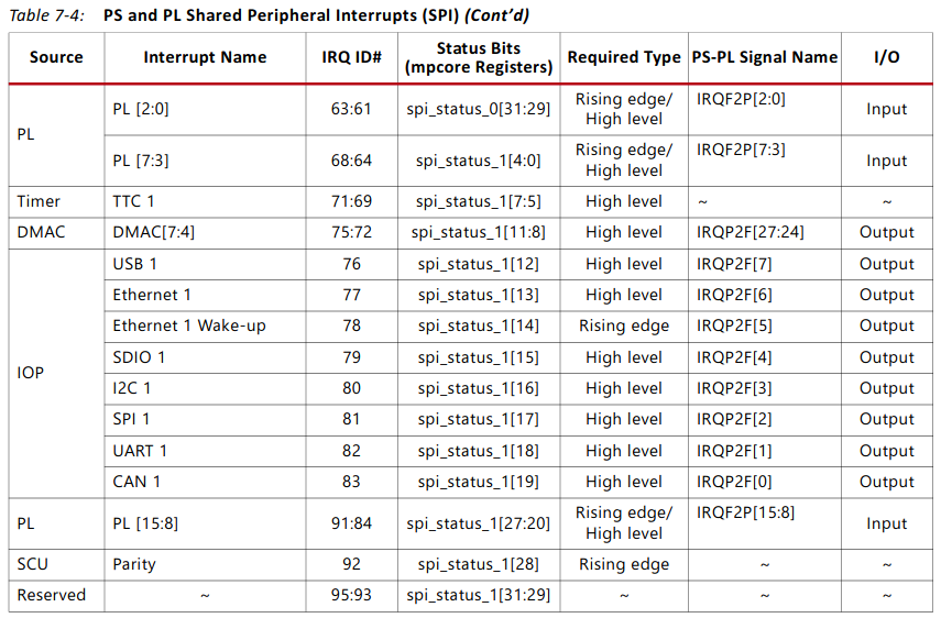
The number the DPU interrupt is connected to would be IRQ_F2P[0], which corresponds to 61 - 32 = 29. This is the number that is needed for the Linux device tree description.
First of all, it is necessary to validate the IP design.
- Right click on the
Block Designworkspace and select the optionValidate Project.
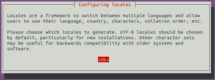
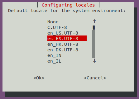
If you are using the keyboard layout es_ES.ud8, you might get the following error printed in the console.
Tcl error in validate procedure while setting value '250.000' on parameter 'CLKOUT1_REQUESTED_OUT_FREQ'. unexpected "," outside function argument list in expression "1000.000 / 2,155".
Tcl error in validate procedure while setting value '450.000' on parameter 'CLKOUT2_REQUESTED_OUT_FREQ'. unexpected "," outside function argument list in expression "1000.000 / 2,155".
This error is being triggered if your keyboard layout has established the , as a decimal separator, rather than the .. The problem can be solved by changing this configuration in the es_ES.ud8 file. Now, open the file:
sudo atom /usr/share/i18n/locales/es_ES
Find the following section of the script, between LC_MONETARY and END LC_MONETARY, change mon_decimal_point to . and mon_thousands_sep to ,. This changes the separators for currency. Now, repeat the operation between LC_NUMERIC and END LC_NUMERIC, changing decimal_point to . and thousand_sep to ,. These section of your file should end up looking as follows.
....

LC_MONETARY
int_curr_symbol      "EUR "
currency_symbol      "<U20AC>"
mon_decimal_point    "."
mon_thousands_sep    ","
mon_grouping         3;3
positive_sign        ""
negative_sign        "-"
int_frac_digits      2
frac_digits          2
p_cs_precedes        0
p_sep_by_space       1
n_cs_precedes        0
n_sep_by_space       1
p_sign_posn          1
n_sign_posn          1
END LC_MONETARY

LC_NUMERIC
decimal_point        "."
thousands_sep        ","
grouping             3;3
END LC_NUMERIC

....
Finally, actualize the modification in the system by executing this command in the terminal.
sudo dpkg-reconfigure locales
- Press
enter.
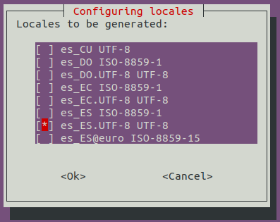
- Press
enter.
- Press
enter.
Now we have to create the HDL wrapper.
- Click the sources tab under the project manager.
- Select the
Hierarchytab at the bottom.
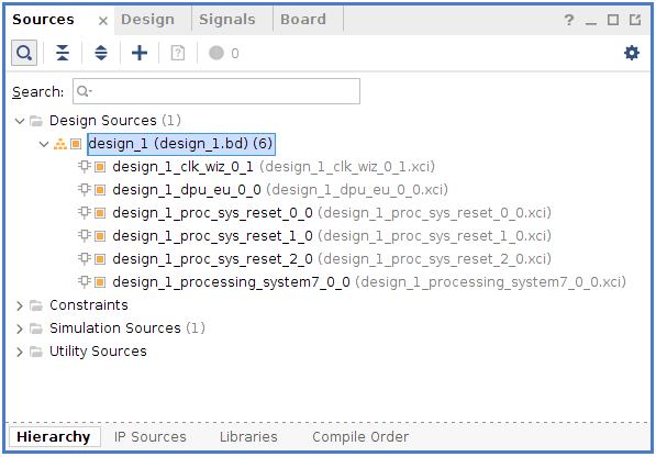
- Under the design sources, right click
desing_1, and select theCreate HDL wrapperoption.
The result of this operation should leave you with a top wrapper with the following name.
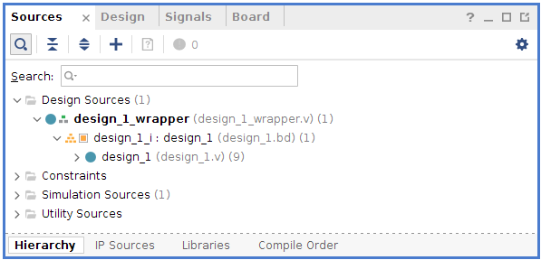
The next step would be to right click design_1_i, and select the Generate output products option. A window will pop-up where the values shown in the following image should be selected.
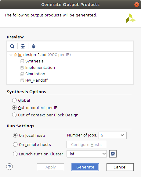
The number of jobs selected will determine the amount of resources your machine uses to perform this operation. Choose a number as high as possible, making sure the machine will be able to handle it.
Finally, click Generate. This step builds all required output products for the selected source. For example, constraints do not need to be manually created for the IP processor system. The Vivado tools automatically generate the XDC file for the processor sub-system when Generate Output Products is selected.
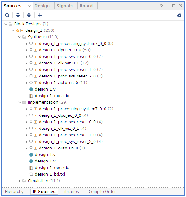
In the sources tab, by clicking IP Sources, next to Hierarchy, the output products generated can be checked.
Now, to finish the generation of the bitstream, follow the next steps.
- Click the
Run Synthesisoption. - Click the
Run Implementationoption. - Click the
Generate bitstreamoption.
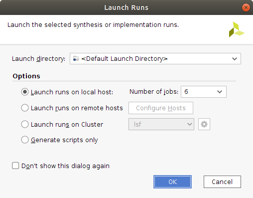
Three windows such as this one shall appear when executing the previous three steps.
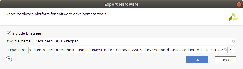
Once the bitstream has been generated, export the model to a .xsa format file.
- Click
File - Click
Export - Select
Export Hardware
Make sure the Include Bitstream option has been checked.