testing - rfrht/FT991A-PAT GitHub Wiki
Testing
Troubleshooting
If your board does not work right off the bat, do not panic. It happens - yes!
In my case, it was because of forgetting entirely to solder the other side of a component, wrong orientation, shorts, insufficient soldering.
How to track the problem?
Start with the basics - Power. Do you have power at the fuse input and output? And the 9V pad? And the 3V pad?
Moving along, check the sw test pad - that's the the RF switch control. You should have no voltage in that line during RX mode. Conversely, it is expected to have around 3V in that test pad when 9V is applied in the TX9 test pad.
Next step, use your VNA as a signal generator (it generates a signal when running its sweeps) at, say 30 MHz, for example (this is the max. frequency that some antenna testers can do and older 'scopes can view too).
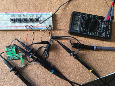
Revision U - Lite in Debug Mode. Click to enlarge
If you have a oscilloscope - use the probe tip ground spring, in order to provide a way cleaner output to your Oscilloscope. Use the ground plane holes to anchor the coil. Use the scale around 200 mV in your scope.
The 1000 pF caps are your friends - They easy to identify, access and are only involved in RF stages. Inject the signal in the IF_IN port and follow it in the first 1000 pF cap, before the RF switch - you should have a strong signal here. That's your reality check. If it is not, you have a problem with your U.FL connector or the signal generator.
So, sanity check done - got the signal, start following it. Start with the 1000 pF cap right after the IF port. Then, the cap right after the RF switch.
To test the J310, remove the 1K resistor near the NCP553 regulator - And then test the left side of the 1000 pF cap between the 2SC5086 and the J310. If you have signal at the left side of the cap, it's your BFR193 soldering. Happened to me, a number of times.
After you got this working, then try the upper side of the 1000 pF cap next to the 82 nH inductor - that's the final DC isolation prior to the SDR out.
Performance
Prior to integrate the panadapter with the radio, besides the obvious testing, I wanted to compare how did the new board performed against the initial Revision I board.
And here are the results!
Equipments
Besides the obligatory multimeter, it helps a lot to have an VNA and knowing how to run it in S21 mode - This is how you can measure the gain and ensure that you have a working board.
Power
The MC78L09A provides max. 100 mA when regulating from 13.8V to 9V - And the NCP553 provides max. 80 mA current to the 3V lines. Expect the 13.8V current draw to be less than 20 mA.
Revision I Board Current Draw Test
RF Performance
Board gain
The panadapter board provides around 7 dB gain around 69.450 MHz:
FT-991A Panadapter RF Gain - Revision U, Lite version
Isolation
The below chart depicts the isolation level between the SDR output and the IF Tap point when the TX9 signal goes high. This chart was obtained while enabling TX9 signal during the VNA sweep. The chart is erratic due to the lack of VNA dynamic range - yet providing a hefty ~ -60 dB signal isolation.
Insertion Loss
This is the board insertion at the input level loss when the TX9 signal (or DIS in full version) is on:
FT-991A Panadapter Insertion Loss. Revision R, Full Version
Previous versions gain figures
BFS17 Gain
Revision I board used G4HUP's LPF design, rolling down around 80-90 MHz. This design was used up to Revision K.
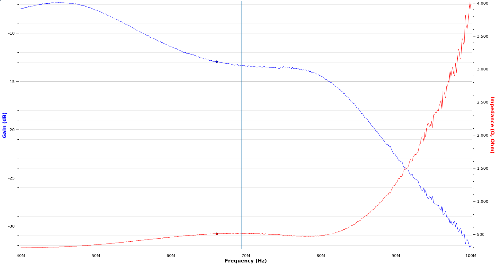
This is the gain figure from Revision I board, using J310 in tandem with BFS17 and G4HUP's LPF:
Revision I gain figures. Frequency of interest in the blue vertical line.
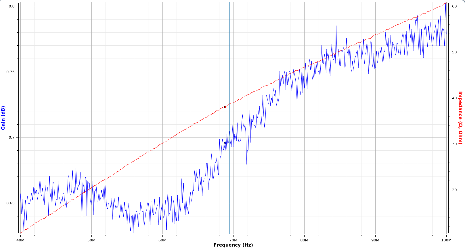
Starting in Revision N, I have removed the original G4HUP LPF. That caused to move the needle from a -11.3 dB gain (well, loss :-P), to some actual gain:
Revision N Gain Figures using BFS17 LNA - Frequency of interest in the blue vertical line.
W00t: 0.7 dB of gain - A lot of improvement when comparing with the previous design!
2SC5086 Gain
Remember, BFS17 was the low noise amplifier in use in the original design by OE2DOR. However, I tried my luck (and my eyes, because it is TINY) with a 2SC5086 LNA instead of BFS17.
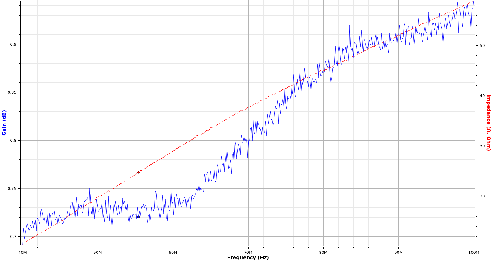
So here is the result:
Revision N and 2SC5086 LNA - Frequency of interest in the blue vertical line.
We moved the needle from 0.7 to 0.8 dB - Not a lot of gain. Then I revamped the board circuits, with several incremental improvements. This is how it looked on the last revision based on 2SC5086:
Revision R gain figures
What does that means in the end?
Over the course of the revisions, by removing unneeded components, testing new boards, PCB tracks, component placement and optimization, we jumped from -13 dB in Rev. I to 7 dB+ in Rev. U.
In revision I, I had to make a lot of use of the SDR's internal amplifier, and I found around 9 dB of gain to be the sweet spot. With Rev. R, I just use 1 dB of gain from the SDR, leaving plenty of room (and less noise) to work weaker signals.
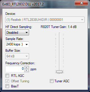
SDR Gain Configuration
Full Version Extras
Passthrough
The Full Version Board also sports a passthrough mode, moving the signal straight from the tap to the SDR, bypassing amplifiers and stuff. Notice that this mode taps (splits) the signal, weakening your radio reception. -3dB loss, right off the bat. The below chart depicts the panadapter board insertion loss - from the IF tap port to the SDR port, in Passhtrough mode.
Insertion Loss in Passthrough mode
At 69.450 MHz I got around -2.25 dB gain.
Band-Pass Filter
After a botched first attempt to build a tentatively 3 MHz wide 69.450 MHz BPF, Karl-Arne helped me designthis filter - The proper way (page 1, page 2).
While originally we projected the filter center frequency around 69.5 MHz, I got a fully working BPF centered at 70 MHz and around 2 MHz wide!
Revision R Full Version Band-Pass Filter - With amplifier
Tips hat to Karl-Arne - Thank you.
