VLSI Design Flow using HDL - mbits-mirafra/digitalDesignCourse GitHub Wiki
VLSI Design Flow
What is VLSI Design Flow?
VLSI (Very Large Scale Integration) design flow is a sequence of steps involved in the design and manufacture of integrated circuits (ICs) or chips. The VLSI design flow typically involves the following steps:
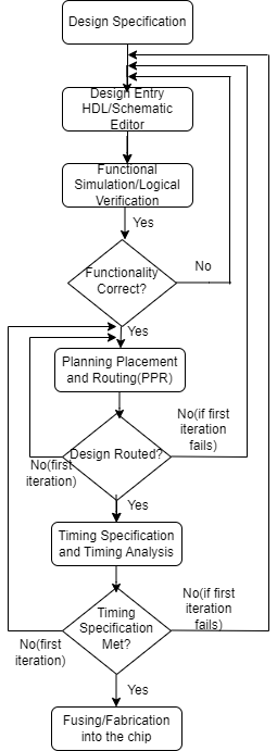
Block diagram
Steps Involved
- Design Specification:-
Design specification refers to a detailed description or requirement of the design attributes that a chip or an electronic system must have to meet
(a) The algorithm to be implemented in detail with mathematical representation: The algorithm specification determines the complexity of the design and gives an idea of number of gates required for the design.
(b) Number of inputs and outputs in the design and number of bits in each to them: Eg: For interfacing an analog to digital converter, all data lines & control line inputs and outputs are provided in the chip.
(C) Number of clock signals to be used in the design.
(d) Maximum clock frequency to be used: It defines the speed of operation of the chip. Maximization of operating speed is one of the main objectives in VLSI design since faster operation needs lesser computation time.
(e) Area of the chip:- For portable type and miniature type of systems, the chip size should be as small as possible. Since million or more number of gates are incorporated on a single chip, so main optimization goal is area of chip in IC design.
(f) Power dissipation in the chip:- The demand for portable semiconductor devices has raised the demand for more power efficient devices. Thus VLSI design has also an objective of Circuit level power saving by modifying circuit design
For Eg:
-
Minimum clock frequency of 100MHz
-
32-bit data bus
-
256KB of Flash memory
-
32KB of RAM
-
Design Entry :- Design entry is the process of describing a digital circuit in a form that can be translated into a physical layout. It is an important step in the VLSI design flow, as the design entry process generates the RTL (Register Transfer Level) code for the logic circuit which forms the base for the implementation process. In design entry, all architectural decisions like number of sub blocks functionality and interconnections such as adders, multipliers, dividers, type of processing, serial or parallel, in each sub blocks.
Design Entry are of two types. (a) Schematic Entry that uses a schematic tool and the designer manually draws the schematic (b) Hardware description language
-
Functional Simulation :- Functional simulation in VLSI refers to the process of verifying the functionality and correctness of a digital circuit design. For example, let's consider the design of a simple adder circuit in VLSI. The adder circuit takes two numbers as input and produces their sum as output. To verify the correctness of the design, functional simulation can be used. This involves writing a testbench code that provides various input values, and then simulating the adder circuit using those input values. The output produced by the circuit is compared with the expected output, and any discrepancies are identified and rectified. This process is repeated until the behavior of the adder circuit matches the desired functionality. If the design is functionally and logically correct the design will be sent to planning placement and routing. If the design functionality is incorrect, the design will be sent back to Design Entry stage to rectify the functionality & logical errors.
-
Planning placement and Routing (PPR): This part is referred to as the vlsi physical design or layout phase. This is the process to determine the physical location of the and make interconnections between them inside the boundary of Vlsi chip. The various phases in layout process are as follows.
(a) Placement :- Placement is the problem of determination of best position of each module, when each module has a fixed shape, area and terminals. Floor planning and placements are very closely related and sometimes combined in computer aided tool.
(b) Routing:- Routing is a method of interconnection of different circuit components, with an aim to minimize the chip area and also reduction of total wire length.
-
Timing specification:- The next phase after successful PPR (planning, placement and routing) is timing simulation. In functional simulation which is done earlier only functional logical correctness of the design is verified. But after the design is fitted into the chip, gate delays comes into account. Timing specification in VLSI refers to the time required for signals to travel through different components of the chip. Gate delays are delays from input of one gate to output of same gate due to propagation time of the gate. If timing specification is not fulfilled then the design is sent to the previous stages for re-routing such that timing specification is met.
-
Fabrication:- Manufacturing the ICs when all the requirements and conditions are properly met.
Applications of VLSI Design Flow
1.Microprocessors and microcontrollers: VLSI design flow is extensively used in the development of microprocessors and microcontrollers, which are the key components in computers and embedded systems. VLSI design flow helps in designing efficient and powerful microprocessors that can perform complex computations and operations.
-
Application-specific integrated circuits (ASICs): ASICs are customized integrated circuits designed for specific applications. VLSI design flow is used to design ASICs that are optimized for particular applications such as automotive, medical, and aerospace industries.
-
System-on-chip (SoC) designs: SoC designs integrate all the necessary components of a system onto a single chip. VLSI design flow is used to design complex SoCs that can perform multiple functions, including communication, computation, and memory storage.
Advantages of VLSI Design Flow
-
Improved design quality: The VLSI design flow follows a structured approach to design, which results in better design quality and reduces the chance of errors in the final product.
-
Reuse of design components: The VLSI design flow enables designers to reuse design components, which reduces the time and effort required for designing complex circuits.
Disadvantages of VLSI Design Flow
- Difficult for beginners: The VLSI design flow requires knowledge of several complex design tools and methodologies, which can be overwhelming for beginners.
- High cost of design tools: The design tools required for VLSI design can be expensive, and the cost of licensing these tools can add up quickly, making it difficult for small companies or individual designers to afford them.
- Time consuming: The VLSI design flow requires complex design verification techniques to ensure that the final design meets the required specifications. This can be time-consuming and requires a thorough understanding of the design tools and methodologies.