SET UP AND HOLD TIME - mbits-mirafra/digitalDesignCourse GitHub Wiki
Set up, Hold Time and propagation delay

Set up time
The amount of time the data at the input must be stable before the active edge of clock. Any violation may cause incorrect data to be captured, which is known as setup violation.
Hold Time
The amount of time the data at the input must be stable after the active edge of clock. Any violation may cause incorrect data to be captured, which is known as Hold violation.
Propagation delay
lets us consider 2 D Flip flop
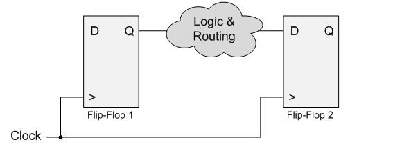
- It takes time for a signal to travel from source to destination i.e FF1 is source and FF2 id destination
- All the flip flop will be made up of nand or nor gate hence after passing through each gates the delay occurs.
- when the propogation delay is longer which means we cant run the clock quickly
suppose a nand gate in logic and routing, the nand gate has its lookup table it goes through it and propagation delay occurs
- Consider a master slave D Latch based Flip flop

let us design a flip flop by using 2 latches, clock is inverted to latch1 so its negative triggered and where as positive triggered at latch 2
now let us draw the timing diagram for the output Q1, Q2 and Q

- we know that latch 1 act as negative latch due to inverter so it triggers at its negative level we can observe in the waveform of Q1
- latch 2 act as positive latch so its going to trigger at positive level this can be observed in Q2
- hence the final output of flip flop Q will be same as Q2 u can see that in above mentioned circuit diagram
Is the output acting as flip flop? we know that whenever the input is given the flip flop will be only considered at positive edges hence we can see the output Q triggers at positive edges hence we obtained flip flop from latches.
- why the Set up and hold time is there in the flip flop?
In the previous example master slave D flip flop there was no propagation delay, but now let us set some delay and check it

As we can see that we gave a propagation delay of 2ns for latch1 so if we give input at D we will getting output after 2ns, lets assume the width of the clock period is 10ns and width of input D to positive edge 2ns mentioned in the diagram.

In order to check why setup time is required we are going to give a delay of 1ns in the input D as shown in the diagram

when delay is given to the input D we already considered the delay of latch will be 2ns we know that latch1 is a negative level triggered but due to delay of 2ns output we are going to get at positive level hence this is known as set up voilation condition.

- Hold time voilation? A inverter is connected to clock of latch1 where we assumed the inverter with a delay of 1ns hence if the input is going to change during that delay then wont be getting a hold time it leads to hold violation.
How to Determine Maximum clock Frequency for a Sequential Circuits?
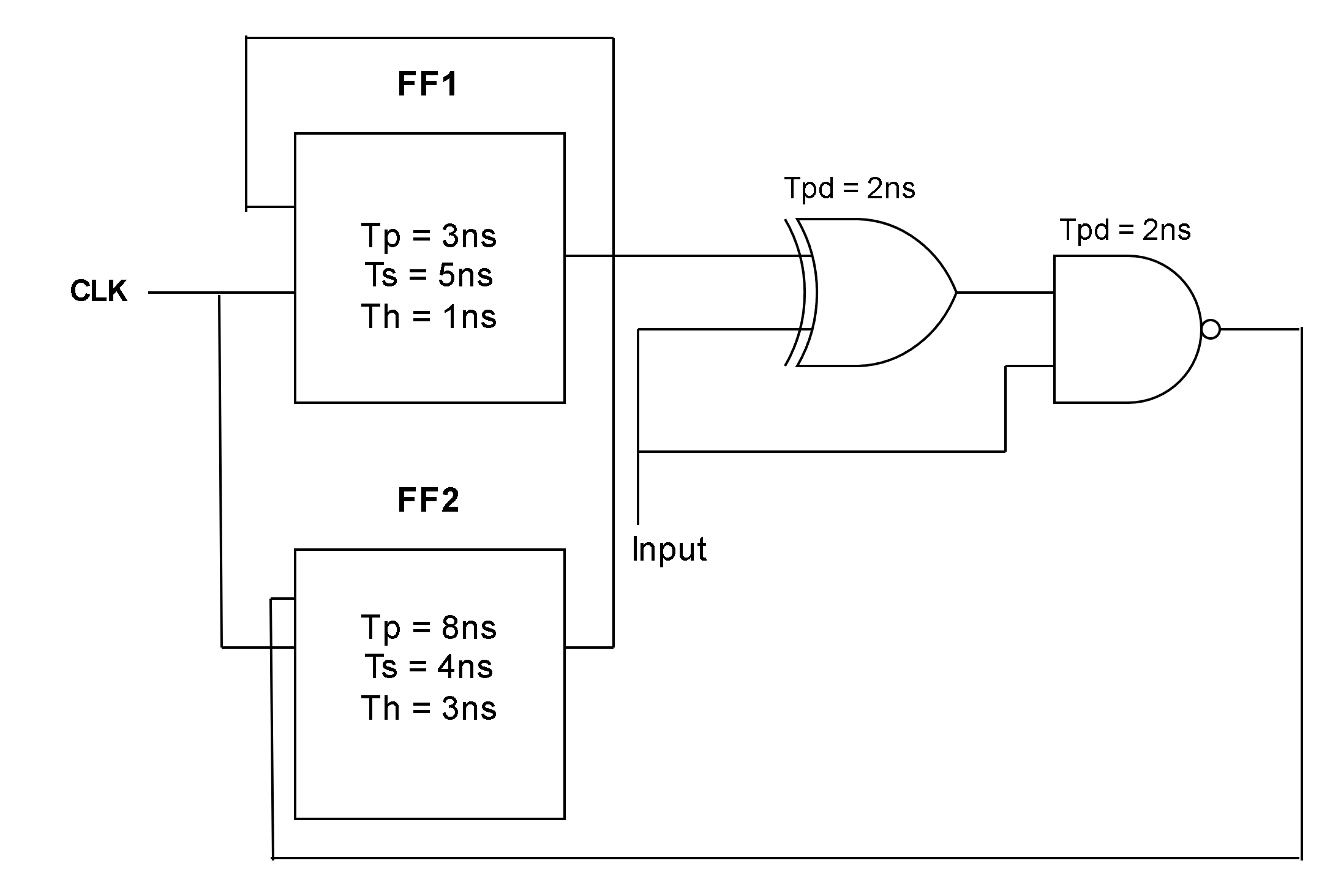
- Firstly we need to find the delay from Flip Flop 1 to 2
- TF12 = Tp(f1) + Tp(xor) + Tp(nand) = 3ns + 2ns + 2ns = 7ns Input going to reach 2 nd flip flop with a delay of 7ns. Hence it will be stable from 7ns to it's setup time so it is 7ns + 4ns (setup time) = 11ns
- Then we need to find the delay from Flip Flop 2 to 1
- From FF2 it reaches to FF1 with a delay of 8 ns hence it will be stable till it's setup time(5ns)
- TF21 = Tp(f2) + ts(f1) = 8ns + 5ns = 13 ns
- Since the TF21 is the largest of the path delays, the minimum clock period for the circuit is Tmin = 13ns and the maximum clock frequency is 1/Tmin = 76.92 MHz.