Registers - mbits-mirafra/digitalDesignCourse GitHub Wiki
What is a Register ?
A register is a type of electronic circuit that can store and manipulate binary data. A register typically consists of a group of flip-flops, where each flip-flop can store a single bit of data. The number of flip-flops in a register determines the number of bits it can store. Registers are used in many digital circuits for a variety of purposes, such as data storage and data transfer.
What is a shift register ?
A shift register is a type of register where data is shifted from one flip flop to another within the register. But this shift of data does not happen by itself. Instead, it needs a clock signal to do so. So for every input clock cycle, the data get shifted from one flip flop to another. Hence the name “Shift Registers”.
There are several types of shift registers, including:
-
Serial-in, serial-out shift register (SISO)
-
Serial-in, parallel-out shift register (SIPO)
-
Parallel-in, serial-out shift register (PISO)
-
Parallel-in, parallel-out shift register (PIPO)
-
Universal shift register (USR)
| Sr.no | Registers |
|---|---|
| 1 | SISO |
| 2 | SIPO |
| 3 | PISO |
| 4 | PIPO |
| 5 | USR |
SISO (Serial in serial out)
What is SISO shift register ?
A SISO (Serial-In, Serial-Out) register is a type of digital circuit that can store a single bit of data and shift it in and out one bit at a time.
The term "serial" refers to the fact that the data is processed one bit at a time, while "in" and "out" refer to the direction of the data flow. In a SISO register, data is input to the circuit through a single input bit, and the output is read from a single output bit. The data is shifted through the register in a sequential manner, with each bit being transferred to the next stage in the register one at a time.
The figure below shows the block diagram of SISO shift register.

Why SISO ?
SISO registers are often used in digital communication systems for storing and transmitting data in serial form. They are also used in microcontrollers and other digital devices for various applications such as data storage, serial communication, and control systems.
Advantages
- Compactness: SISO registers require less physical space to implement compared to other types of registers such as parallel-in, parallel-out (PIPO) registers. This makes them suitable for applications where space is a constraint.
- Power efficiency: SISO registers consume less power compared to other types of registers, making them suitable for applications where power consumption is a concern.
- Simplicity: SISO registers have a simple structure, consisting of only one input and one output. This makes them easy to design and implement.
Disadvantages
- Slow data transfer: SISO registers transfer data one bit at a time, which can be slow for large amounts of data. This makes them less suitable for applications that require high-speed data transfer.
- Limited capacity: SISO registers can only store a single bit of data, which limits their capacity. To store larger amounts of data, multiple SISO registers must be cascaded together, which can increase complexity and reduce speed.
When SISO is used ?
SISO (Serial-In Serial-Out) shift register is used when data is to be shifted through a circuit one bit at a time in a serial format, and there is no need to output the data in parallel.
-
Serial data transmission: SISO shift registers can be used in communication systems to transmit data serially over a single data line.
-
Data processing: SISO shift registers can be used in digital signal processing to perform operations such as delay.
-
Counter circuits: SISO shift registers can be used in counter circuits to increment or decrement a count value by one bit at a time.
How SISO works ?
SISO Shift register diagram is shown below which includes 4-D flip-flops. The connection of these FFs can be done by connecting the one Flip Flops output to the next flip flop input. So these FFs are synchronous through each other because the equal CLK signal is applied in each Flip Flop.
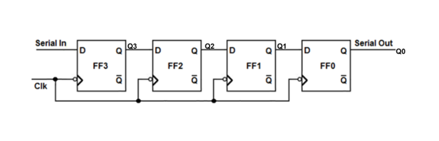
This is a shift right mode circuit which means when the data i/p is given at the left end of the flip flop then the stored bit can be shifted to the right side to generate serial output.
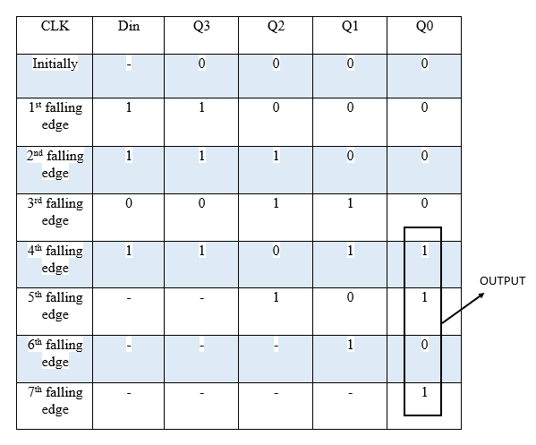
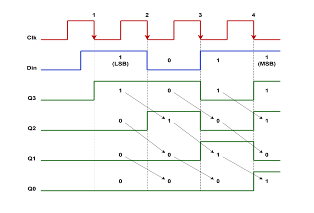
- Shifting by taking the LSB first :
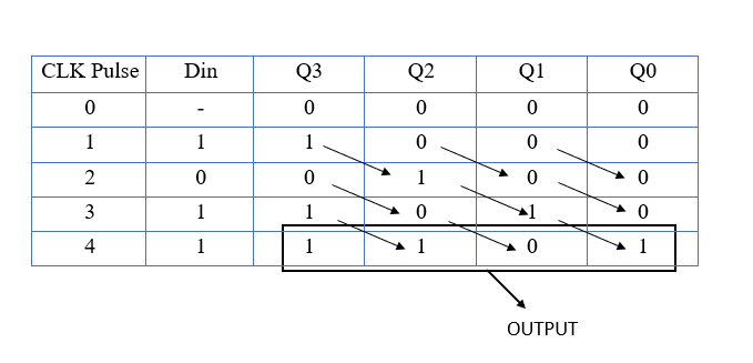
- Initially, the circuit must be set to reset mode so the output of every register will be ‘0’, so the output provided by all the registers will be “0000”.
- Let us take an example of the 1011 binary number. The input is applied to shift register by taking LSB first and lastly the MSB.
- In this example the LSB bit is "1" and the MSB bit is "1". First, the high signal (LSB bit) is used as input to the first flip-flop D3, then D3=1. But mainly all D FF outputs will be 0. So D2=D1=D0=0. D3 will cause "Q3" to be a "1" when the D3 input is a high signal (1). Therefore, the overall o/p for the 1st falling edge will become 1000.
- Similarly, the next bit (logic 1) is applied as serial input to the serial input pin of FF3.Therefore Q3 will be set (logic 1). The previous output of Q3 is connected to FF2 therefore Q2 will be set (logic 1) and all the other outputs still remains at logic 0. Thus the overall o/p for the 2nd falling edge will get as “1100”.
- On the third clock pulse the next bit (logic 0) is applied as serial input to the serial input pin of FF3 therefore Q3 will be set (logic 0). The previous output of Q3 is connected to FF2 therefore Q2 will be set (logic 1). The previous output of Q2 is connected to FF1 therefore Q1 will be set (logic 1) and all the other outputs still remains at logic 0. So the overall o/p for the 3rd falling edge will get as “0110”.
- On the fourth clock pulse the next bit (logic 1) is applied as serial input to the serial input pin of FF3 therefore Q3 will be set (logic 1). The previous output of Q3 is connected to FF2 therefore Q2 will be set (logic 0). The previous output of Q2 is connected to FF1 therefore Q1 will be set (logic 1) and the previous output of Q1 is connected to FF0 therefore Q0 will be set (logic 1). Finally, SISO shift register store 1011 bit.
- By applying the fifth clock pulse, FF0 will produce output of 1 from the Q0. Similarly by applying next clock pulse we will get the next bit stored in the FF0. Further we need to apply the clock pulses until we get all the stored bit in the output.
- Therefore, the 4-bit SISO shift register requires seven clock pulses in order to produce the valid output. Similarly, the N-bit SISO shift register requires 2N-1 clock pulses in order to shift ‘N’ bit information.
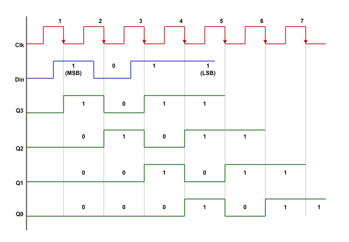
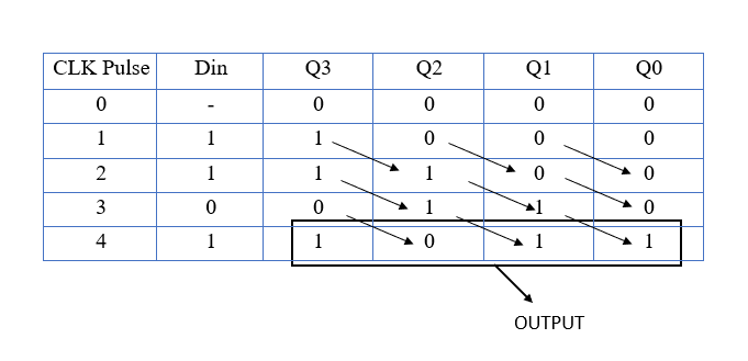
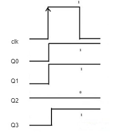
SISO Shift register truth table is shown below by taking the LSB first.
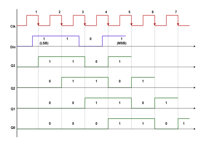
By considering the above truth table, the SISO shift register waveform representation will be like the following.
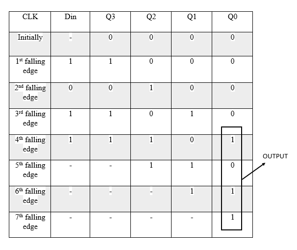
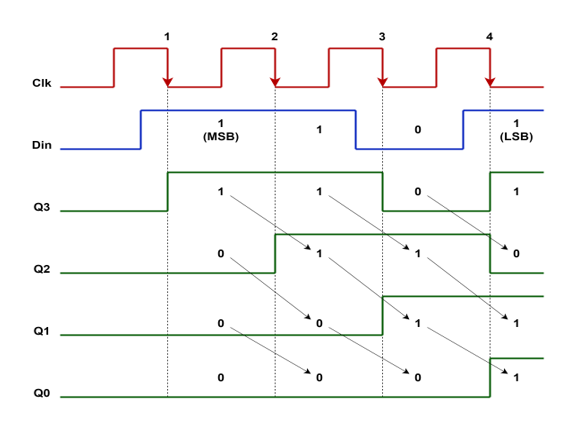
- Shifting by taking the MSB first :
- Initially, the circuit must be set to reset mode. So the output provided by all the registers will be “0000”.
- Let us take an example of the 1011 binary number. The input is applied to shift register by taking MSB first and lastly the LSB.
- In this example the MSB bit is "1" and the LSB bit is "1". First, the MSB bit is used as input to the first flip-flop, then D3=1. But mainly all D FF outputs will be 0. So D2=D1=D0=0. D3 will cause "Q3" to be a "1" when the D3 input is a high signal (1). Therefore, the overall o/p for the 1st falling edge will become 1000.
- Similarly, the next bit (logic 0) is applied as serial input to the serial input pin of FF3.Therefore Q3 will be set (logic 0). The previous output of Q3 is connected to FF2 therefore Q2 will be set (logic 1) and all the other outputs still remains at logic 0. Thus the overall o/p for the 2nd falling edge will get as “0100”.
- On the third clock pulse the next bit (logic 1) is applied as serial input to the serial input pin of FF3 therefore Q3 will be set (logic 1). The previous output of Q3 is connected to FF2 therefore Q2 will be set (logic 0). The previous output of Q2 is connected to FF1 therefore Q1 will be set (logic 1) and all the other outputs still remains at logic 0. So the overall o/p for the 3rd falling edge will get as “1010”.
- On the fourth clock pulse the next bit (logic 1) is applied as serial input to the serial input pin of FF3 therefore Q3 will be set (logic 1). The previous output of Q3 is connected to FF2 therefore Q2 will be set (logic 1). The previous output of Q2 is connected to FF1 therefore Q1 will be set (logic 0) and the previous output of Q1 is connected to FF0 therefore Q0 will be set (logic 1). Finally, SISO shift register store 1101 bit & shows in the o/p.
SISO Shift register truth table is shown below by taking the MSB first.
By considering the above truth table, the SISO shift register waveform representation will be like the following.
SIPO (Serial in parallel out)
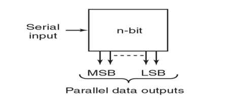
What is SIPO shift register ?
The SIPO register is a type of shift register in digital electronics. The term "SIPO" stands for "Serial-In Parallel-Out", which describes its behavior.
In a SIPO register, data is entered serially, one bit at a time, through a single input called the "data" or "serial" input. The register holds the data and shifts it one bit at a time to the parallel output pins. Once all the bits have been shifted in, they can be read out in parallel from the output pins.
The figure below shows the block diagram of SIPO shift register.
Why SIPO ?
SIPO registers are commonly used in digital circuits for a variety of purposes, including data storage, data transfer, and signal processing. They are often used in microcontrollers, digital signal processors, and other integrated circuits to implement functions such as shift, rotate, and serial-to-parallel conversion.
Advantages
- Reduced number of pins: SIPO registers require only one input pin and a few output pins, which reduces the overall number of pins needed for a circuit compared to using parallel registers.
- Cost-effective: SIPO registers are generally less expensive to produce than parallel registers, which makes them a cost-effective option for many applications.
Disadvantages
- Slow data transfer: Since data is shifted in one bit at a time, the transfer rate is relatively slow compared to parallel registers.
- Limited data width: SIPO shift registers are limited in terms of the number of bits they can hold at a time. For larger data sets, multiple shift registers must be cascaded together, which can add complexity to the circuit design.
When SIPO is used ?
A SIPO (Serial-In Parallel-Out) shift register is used when data needs to be shifted through a circuit in a serial format and then output in parallel.
- Serial-to-parallel conversion: SIPO shift registers can be used to convert serial data to parallel data for further processing or display.
- Data storage: SIPO shift registers can be used to store data in a compact format and then output the data in parallel when needed.
How SIPO works ?
SIPO Shift register diagram is shown below which includes 4-D flip-flops connected in cascaded form i.e., output of one D flip-flop is connected as the input of next D flip-flop. All these flip-flops are synchronous with each other as same clock signal is applied to each one.
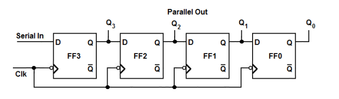
In this shift register, bits can be sent serially from the input of left most D flip-flop. Hence, this input is also called as serial input. For every negative edge triggering of clock signal, the data shifts from one stage to the next. In this case, the outputs of each D flip- flop can be accessed in parallel. So, parallel outputs are obtained from this shift register.
- Shifting by taking the LSB first :
- Initially, all the output will become zero. So without CLK pulse, all the data will become zero.
- Let us take an example of the 1101 binary number. The input is applied to shift register by taking LSB first and lastly the MSB.
- If we apply the first clock pulse ‘1’ to the first flip flop , the data to be entered into the FF3 and Q3 becomes ‘1’, and remaining all the outputs like Q2, Q1 and Q0 will become zero. So the first data output is ‘1000’.
- If we apply the second clock pulse as ‘0’ to the first flip flop then Q3 becomes ‘0’, Q2 becomes ‘1’, Q1 becomes ‘0’ and Q0 becomes ‘0’. So the second data output will become ‘0100’ due to the shift right process.
- If we apply the third clock pulse as ‘1’ to the first flip flop then Q3 becomes ‘1’, Q2 becomes ‘0’, Q1 becomes ‘1’ and Q0 becomes ‘0’. So the third data output will become ‘1011’ due to the shift right process.
- If we apply the fourth clock pulse as ‘1’ to the first flip flop then Q3 becomes ‘1’, Q2 becomes ‘1’, Q1 becomes ‘0’ and Q0 becomes ‘1’. So the fourth data output will become ‘1101’ due to the shift right process.
- The 4-bit SIPO shift register requires four clock pulses in order to produce the valid output. Similarly, the N-bit SIPO shift register requires N clock pulses in order to shift ‘N’ bit information.
SIPO Shift register truth table is shown below by taking the LSB first.
By considering the above truth table, the SIPO shift register waveform representation will be like the following.
If we shift the LSB (Least Significant Bit) first in a SIPO (Serial-In, Parallel-Out) shift register, we will get the same output sequence as the input sequence.
- Shifting by taking the MSB first :
- Initially, all the output will become zero. So without CLK pulse, all the data will become zero.
- Let us take an example of the 1101 binary number. The input is applied to shift register by taking MSB first and lastly the LSB.
- If we apply the first clock pulse ‘1’ to the first flip flop , the data to be entered into the FF3 and Q3 becomes ‘1’, and remaining all the outputs like Q2, Q1 and Q0 will become zero. So the first data output is ‘1000’.
- If we apply the second clock pulse as ‘1’ to the first flip flop then Q3 becomes ‘1’, Q2 becomes ‘1’, Q1 becomes ‘0’ and Q0 becomes ‘0’. So the second data output will become ‘1100’ due to the shift right process.
- If we apply the third clock pulse as ‘0’ to the first flip flop then Q3 becomes ‘0’, Q2 becomes ‘1’, Q1 becomes ‘1’ and Q0 becomes ‘0’. So the third data output will become ‘0110’ due to the shift right process.
- If we apply the fourth clock pulse as ‘1’ to the first flip flop then Q3 becomes ‘1’, Q2 becomes ‘0’, Q1 becomes ‘1’ and Q0 becomes ‘1’. So the fourth data output will become ‘1011’ due to the shift right process.
SIPO Shift register truth table is shown below by taking the MSB first.
By considering the above truth table, the SIPO shift register waveform representation will be like the following.
If we shift the MSB (Most Significant Bit) first in a SIPO (Serial-In, Parallel-Out) shift register, we will not get the same output sequence as the input sequence. When the MSB is shifted first, the input data is shifted into the highest-order bit of the shift register and the remaining bits are shifted to the lower-order positions. Therefore, the output sequence will be in reverse order compared to the original input sequence.
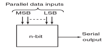
PISO (parallel in serial out)
What is PISO shift register ?
The shift register, which allows parallel input (data is given separately to each flip flop and in a simultaneous manner) and produces a serial output is known as Parallel-In Serial-Out shift register.
The figure below shows the block diagram of PISO shift register
Why is PISO used
A PISO shift register is used to change the data from parallel to serial form. This kind of shift register is used to generate time delay for digital circuits. PISO shift register's practical application is to read numerous switch closures into a chip on a few pins. This register reads the data into a memory chip
Advantages
- Flexibility: PISO shift registers offer greater flexibility in data transfer operations than other shift register types. They can be used to transfer data in both directions, allowing them to be used for a variety of different applications.
- Compatibility: PISO shift registers are compatible with a wide range of digital systems, making them a versatile and widely used component in electronics design.
For example, a PISO shift register can be used as an input device to capture data from a set of switches, which can then be sent to a microcontroller or FPGA for processing.
- Cost-Effective: PISO shift registers are relatively low cost and can be easily integrated into digital circuits. This makes them an attractive option for designers looking to reduce the cost of their designs.
Disadvantages
- Propagation Delay: PISO shift registers can experience a propagation delay in the transfer of data from the parallel input to the serial output, which can limit the speed at which data can be transferred.
- Additional Circuitry: PISO shift registers may require additional circuitry to be added to digital systems to handle data transfer operations, increasing the complexity and cost of the design.
- Timing Issues: PISO shift registers require careful attention to timing to ensure that data is transferred correctly, which can make the design process more challenging.
when is PISO shift registers used
-
Serial Data Transmission: PISO shift registers are often used in digital systems to convert parallel data into a serial format for transmission over a serial communication interface, such as UART or SPI. This is useful when transferring large amounts of data between digital systems, as serial communication interfaces typically have a lower pin count and require less wiring.
-
Serial Memory Devices: PISO shift registers are also used in some types of serial memory devices, such as shift register memory. These devices store data in a serial format, with the PISO shift register used to shift data in and out of the memory device.
-
Digital Signal Processing: PISO shift registers are used in digital signal processing circuits to shift and process data in real-time. This can include operations such as digital filtering, frequency analysis, or time-domain signal processing.
PISO shift registers can be used to convert the parallel pixel data into a serial stream, which can then be transmitted or stored more efficiently.
How PISO works
The figure given below shows a 4-bit Parallel In – Serial Out (PISO) shift register which consists of four D flip-flops and an AND-OR logic to determine whether data will load in parallel, or stored data will shift to right
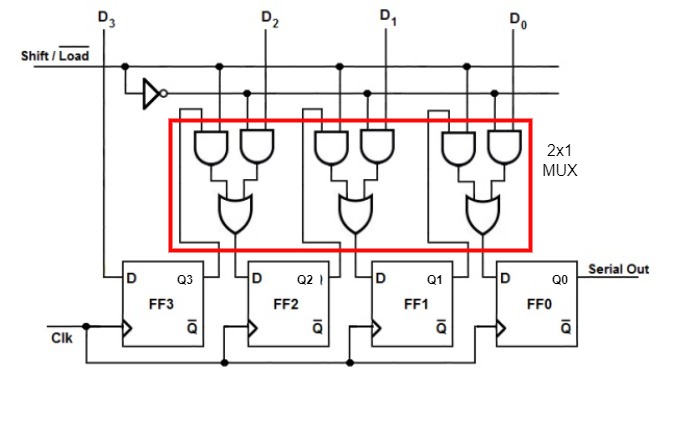
o Here the clock input is directly connected to all the flip flops but the input data is connected individually to each flip flop through a multiplexer at the input of every flip flop.
o The output of the previous flip flop and parallel data input are connected to the input of the MUX and the output of MUX is connected to the next flip flop. All these flip-flops are synchronous with each other since the same clock signal is applied to each flip flop.
o Here shift/load ‘ control line is used to select the functionality of the shift register amongst shift or load at a given instant of time. This is because when the shift/load ‘ line is made low, second AND gates of all the combinational circuits become active while first AND gates become inactive.
o Thus the bits of the input data word (Data in) appearing as inputs to the second AND gates are passed on as the outputs of OR gates at each individual combinational circuit. This causes the individual bits of the Data in to be loaded/stored into respective flip-flops at the appearance of first leading edge of the clock (except the bit D3 which gets directly stored into FF1 at the first clock tick). This indicates that all the bits of the input data word are stored into the register components at the same clock tick.
o shift/load‘ line is driven high to activate first and gates of the combinational circuits which inturn disables the second and gates. This causes output bit of each flip-flop to appear at the output of the OR gate driving the very-next flip-flop (except the last flip-flop FF0) At this stage, if the rising edge of the clock pulse appears, then Q1 appears at Q2, Q2 appears at Q3, … and Qn-1 appears at Qn.
o This is nothing but right-shift of the data stored within the register by one-bit. Similarly it is seen that for each of the further clock pulses applied, one bit exits the PISO shift register through the output pin of nth flip-flop (Data out = Qn of FF0), which is nothing but the serial output. Thus one requires n clock cycles to obtain the entire n-bit input data word as a serial output of PISO shift register.
The combinational circuit is responsible for performing any required logic operations on the input data and arranging it in the correct order for serial transmission.
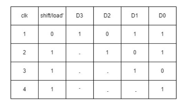
Truth table for parallel in serial out register when right shift is done is given below
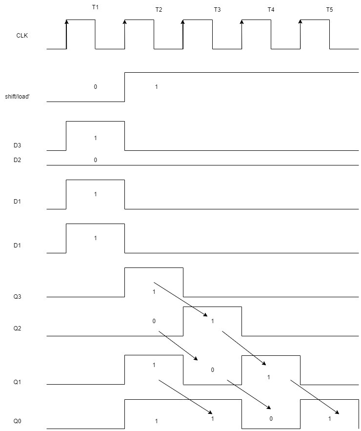
waveform
PIPO (Parallel in parallel out)
Parallel In Parallel Out (PIPO) shift registers are the type of storage devices in which both data loading as well as data retrieval processes occur in parallel mode.
Block diagram of PIPO shift register

why is PIPO shift registers used
One reason why pipo shift registers are used is their ability to store and manipulate large amounts of data quickly and efficiently. By using multiple flip-flops, a pipo shift register can store and shift several bits of data simultaneously, enabling fast parallel operations.
Another reason why pipo shift registers are used is their flexibility in implementing various logic functions. They can be used to perform operations such as serial-to-parallel conversion, parallel-to-serial conversion, and more. This makes them a versatile tool for designing and implementing various digital systems.
Advantages
- Error correction: Pipo shift registers can be used to implement error correction codes, which can improve the reliability and accuracy of digital data transmission and storage.
- High speed: Pipo shift registers can perform parallel operations at high speed, allowing them to quickly process and manipulate large amounts of data.
- Easy interface: Pipo shift registers can easily interface with other digital components and systems, making them ideal for use in communication systems, microcontrollers, and other digital devices.
- Low power consumption: Pipo shift registers can operate at low power levels, making them suitable for use in battery-powered devices and other low-power applications.
Disadvantages
-
Limited data capacity: Pipo shift registers can only store and process a fixed number of bits of data at a time, which can limit their usefulness in applications that require larger amounts of data storage and processing.
-
Complexity: Pipo shift registers can be complex to design and implement, particularly when large numbers of registers are needed.
-
Propagation delay: Pipo shift registers can introduce propagation delays in digital circuits, which can impact their performance in high-speed applications.
when is PIPO shift register used
Pipo (parallel-in, parallel-out) shift registers are used in a wide variety of digital electronics and communication systems where high-speed data processing, storage, and manipulation are required.
-
Memory systems: Pipo shift registers can be used to implement memory systems for digital devices, such as microcontrollers and data storage devices.
-
Logic circuits: Pipo shift registers can be used to implement various logic circuits, such as counters, shifters, and multiplexers.
How does PIPO shift registers work
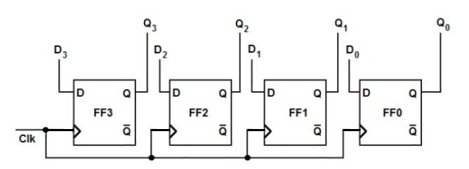
4 bit pipo shift register
Figure shows a PIPO register capable of storing 4-bit input data word (Data in). Here each flip-flop stores an individual bit of the data in appearing as its input (FF3 stores D3 appearing at D; FF2 stores D2 appearing at D; FF1 stores D1 appearing at D1;FF0 stores D0 appearing at D) at the instant of first clock pulse. Further, at the same instant, the bit stored in each individual flip-flop also appears at their respective output pins (Q0 =D0 ;Q1 = D1; Q2 = D2 Q3 = B3). This indicates that both data storage as well as data recovery occur at a single (and at the same) clock pulse in PIPO registers.
which means that as soon as the 4 bit parallel data is given it is stored in the respective 4 D flipflops and at the first clock pulse itself all the bits are given as output in parallel.
Truth table for PIPO shift register :

Waveform for PIPO shift registers :
USR-(Universal Shift Register)
What is USR?
USR is a special type of register that can load the data in a parallel way and shift that data in both directions, i.e., right and left. Hence it can be considered as bidirectional shift register capable of parallel loading. It is called "universal" because it can handle different types of data formats such as serial, parallel, or even a combination of both. The universal shift register typically consists of a set of flip-flops (usually D flip-flops), which store the data bits and can be connected in a series to create a shift register.
Why USR is used?
USR can perform serial to parallel, parallel to serial, parallel to parallel and serial to serial operations. Hence, It is an all in one operational circuit and can be used in general applications. It is used in temporary storage of data before it is processed or transferred to another circuit, data transfer involving serial-to-parallel and parallel-to-serial data conversion, in signal processing operations such as filtering and frequency multiplication, and in encryption and decryption algorithms.
Advantages
- Versatility: Universal shift registers are versatile and can be used for a wide range of digital applications, including data storage, transfer, and signal processing.
- Flexibility: They offer flexibility in terms of the direction and amount of data shifting. This flexibility allows for easy customization of digital circuits to suit specific needs.
- Low Power Consumption: They consume low power, making them suitable for battery-powered devices such as mobile phones and laptops.
- Compact Size: Universal shift registers are typically small in size, which makes them suitable for integration into complex digital circuits.
Disadvantages
- Complexity: Universal shift registers are relatively complex circuits that require careful design and implementation. This complexity may increase the likelihood of errors and decrease the reliability of the circuit.
- Propagation Delay: The shifting of data through the circuit may result in propagation delay, which can affect the timing of the entire system. This delay can be minimized through careful design, but it can be a challenge in some applications.
When USR is used?
- Digital Signal Processing: Universal shift registers can be used in digital signal processing (DSP) applications, where they are used to implement various DSP algorithms such as FIR and IIR filters, discrete Fourier transforms (DFTs), and signal decimation.
- Data Compression: Universal shift registers can be used in data compression algorithms, where they are used to perform bit manipulation and data reordering to reduce the size of the data.
- Test Pattern Generation: Universal shift registers can be used in the generation of test patterns for digital circuits. They can be used to shift a sequence of test patterns into a digital circuit to test its functionality.
How USR works?
Block diagram:
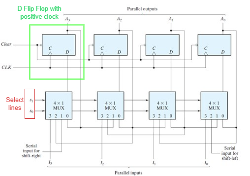
Universal shift registers are capable of performing 3 operations as listed below.
- Parallel load operation – stores the data in parallel as well as the data output is in parallel
- Shift left operation – stores the data and transfers the data shifting towards left in the serial path
- Shift right operation – stores the data and transfers the data by shifting towards right in the serial path.
Truth table:
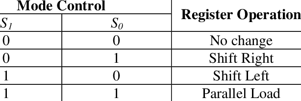
Depending on the select lines the operation of USR varies:
- For 00 combination of select lines, the input (zeroth pin of multiplexer) is connected to the output pin of the corresponding flip-flop.
- For 01 combination of select lines, the input (first pin of multiplexer) is connected to the output of the very-previous flip flop which facilitates the right shift.
- For 10 combination of select lines , the input (second pin of multiplexer) is connected to the output of the very-next flip-flop which facilitates the left shift.
- For 11 combination of select lines, the input (third pin of multiplexer) is connected to the individual bits of the input data which facilitates parallel loading. Thus depending on the select lines the shift register operation is facilitated.