Introduction behavior, logic and physical synthesis - mbits-mirafra/digitalDesignCourse GitHub Wiki
Introduction to Behavioral Synthesis
Behavioural synthesis is a process used in VLSI (Very Large Scale Integration) design that transforms a high-level description of a circuit's behaviour into a low-level representation that can be implemented in hardware.
The goal of behavioural synthesis is to automatically generate an efficient hardware implementation of a circuit from a behavioural description that is written in a hardware description language (HDL) such as VHDL or Verilog. Behavioural synthesis has several advantages over manual design methods, including increased productivity, reduced design time, and improved quality of the final design.
The behavioural synthesis process involves several steps,
- High-level synthesis: This step involves transforming a high-level design specification into an abstract form that captures the essential functionality of the circuit. An abstract representation is a simplified or generalized description of a complex system or concept that captures its essential features without including unnecessary details.
For example, an abstract representation of a digital signal processing (DSP) circuit might include descriptions of its main computational blocks, such as adders, multipliers, and filters, without specifying the exact implementation details of each block.
This abstract representation can then be further refined into a Register-Transfer Level (RTL) representation that includes details such as clock cycles, control signals, and data paths, which are needed for implementation in hardware. This is done using tools such as C-to-RTL compilers, HLS (High-Level Synthesis) tools, or algorithmic synthesis tools.
- RTL synthesis: TRTL synthesis, also known as logic synthesis, is the process of converting an abstract representation of a circuit, typically expressed in a high-level hardware description language (HDL) such as Verilog or VHDL, into a Register-Transfer Level (RTL) description.
An RTL description is a lower-level hardware description that describes the behaviour of the circuit in terms of its registers, combinational logic, and interconnections.
During RTL synthesis, the input HDL description is analyzed and optimized for various metrics such as area, power, and timing. The HDL code is also checked for correctness, and any issues such as hazards or race conditions are addressed.
The output of RTL synthesis is a netlist that describes the circuit in terms of its RTL components, including registers, logic gates, and other components.
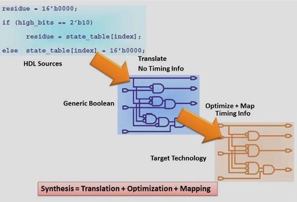
- Logic synthesis: This involves mapping the RTL representation of the circuit to a library of standard cells, which are basic building blocks of digital circuits such as gates, flip-flops, and multiplexers.
The output of logic synthesis is a netlist of gates, which can be used for further optimization, simulation, and verification.
In addition to mapping RTL to gates, logic synthesis may also perform additional optimizations such as technology mapping, which maps the gates to the specific technology library for the target technology, and power optimization, which reduces the power consumption of the circuit. The final output of the logic synthesis process is a gate-level netlist that describes the circuit in terms of its gates and interconnections.
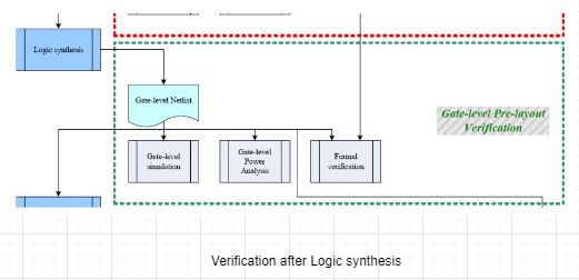
- Verification: The purpose of verification after logic synthesis is to ensure that the gate-level netlist correctly implements the intended functionality of the original design. This involves verifying that the gate-level netlist meets certain timing constraints, such as setup and hold times, and that it does not introduce any new functional errors or glitches.
-
The verification process typically involves running simulations on the gate-level netlist using specialized verification tools. The simulation results are compared against the expected results, which are derived from the original design specification.
-
If any errors or discrepancies are found, they must be corrected and the verification process must be repeated until the gate-level netlist is proven to be functionally correct. Once the verification process is completed successfully, the gate-level netlist can be used as the basis for physical design and layout.
Overall, behavioural synthesis is an important tool for digital system designers, as it allows them to automatically generate complex hardware designs from high-level behavioural descriptions.
This can significantly reduce the time and effort required to design and implement digital systems, while also improving the quality and reliability of the final product.
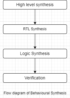
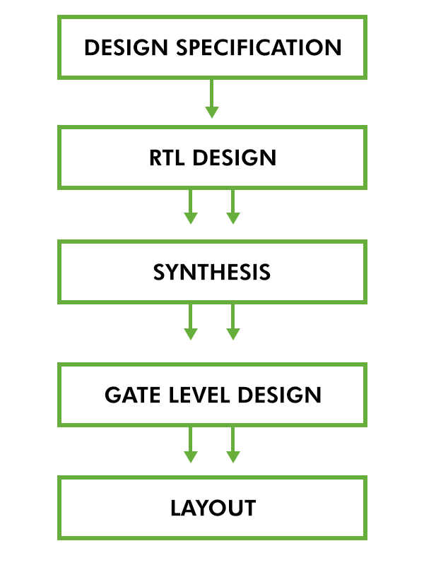
Flow diagram of Behavioral Synthesis
LIMITATIONS:
-
Difficulty in handling complex circuits: Behavioral synthesis is suitable for relatively simple circuits with a limited number of functional blocks. For complex circuits, the behavioural synthesis process can become computationally expensive, making it difficult to achieve reasonable synthesis times.
-
Difficulty in handling specific hardware features: Behavioral synthesis is not well-suited for designing circuits that rely on specific hardware features, such as asynchronous or mixed-signal circuits. These circuits require more detailed control over the implementation details, which is difficult to achieve with behavioural synthesis.
-
Difficulty in handling complex protocols: Behavioral synthesis is not well-suited for designing circuits that require complex communication protocols, such as networking or communication circuits. These circuits require more detailed control over the communication protocol, which is difficult to achieve with behavioral synthesis.
Introduction to logical synthesis
- Logic synthesis is the process of automatic production of logic components, in particular digital circuits.
- It is a subject about how to abstract and represent logic circuits, how to manipulate and transform them, and how to analyse and optimize them.
- Logic synthesis is the process that takes place in the transition from the register-transfer level to the transistor level. It bridges the gap between high-level synthesis and physical design automation.
- The physical positions and interconnections of the gate layouts are then further determined at the time of physical design.
Logic synthesis overview
Drawbacks in the existing system:
- Code and logic designs had to be manually written on paper.
- There was a limitation on the number of variables that could be used in the logic design.
- Could only design very small and simple designs that could not perform complex problems.
For greater performance, we have to manufacture more compact designs and put gates and other components as close as they can be so as to reduce the distance between them. This will ultimately lead to faster conduction, reduce delays, and will cause higher frequency operation.
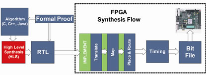
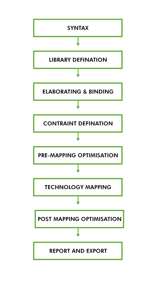
Logic Synthesis Flow
-
Syntax Analysis: Takes input of HDL files and checks for syntax errors.
-
Library Definition: Provides and allocates standard cells and IP libraries.
-
Elaboration and Binding: Translates RTL into the Boolean structure. Binds all cells and makes libraries available.
-
Constraint Definition: For building a customized and specific chip, we need to define constraints according to which the chip will function. For e.g. clock frequency, power efficiency, etc.
-
Pre-mapping Optimization: It performs mapping to generic cells in the library.
-
Technology Mapping: Performs mapping of the generic libraries to technology libraries.
-
Post-mapping Optimization: Changes gate designs to meet constraints.
-
Report and export: Give out the end results with reports on timings and export.
Physical synthesis
Physical synthesis is the process of transforming a Register Transfer Level (RTL) design into a physical implementation of that design, which includes details such as placement of logic gates, routing of signals, and optimization of timing constraints.
Physical synthesis tools take the RTL description of the design and use algorithms to perform various tasks such as technology mapping, placement and routing, timing optimization, power optimization, and more.
Tools are used to ensure that the design meets the desired performance goals such as area and power consumption.
When is physical synthesis used?
Physical synthesis is required when designing complex digital circuits with high-performance requirements. It is particularly useful for designs that are timing-critical, power-sensitive, and require small area utilization. Examples include microprocessors, digital signal processors, ASICs, and FPGAs. Physical synthesis ensures that the logical design is mapped to an optimized physical implementation that meets the design goals and constraints.
The physical synthesis process includes the following steps:
Partitioning
Partitioning is an important step in physical synthesis, which involves dividing the design into smaller, manageable pieces or partitions normally called macros. The goal of partitioning is to simplify the physical implementation process, reduce the overall design complexity, and improve the quality of results.
The partitioning process is typically automated using physical synthesis tools, which use algorithms to analyze the design and determine the best partitioning strategy based on various factors such as the size of the design, timing constraints, and physical layout.
Floor Planning and Placement
Once the design has been partitioned into macros (like rooms in our house), the next step is to place these macros in an optimized way. Just as we would like to have some kind of flow in our living rooms, the goal is to place structure with connections close together .
Floor planning can be done manually or with the help of automated tools. Automated floor planning tools use algorithms to optimize the placement of the functional blocks and reduce the overall chip size.
Placement is the process of determining the physical location of each functional block on the chip. The goal of placement is to minimize the overall wire length and optimize the timing and power requirements of the design.
Clock tree synthesis
Clock tree synthesis (CTS) is a crucial step in the physical design flow of digital integrated circuits (ICs), where a clock distribution network or tree is constructed to ensure that the clock signal is distributed uniformly and with minimum skew to all the sequential elements (such as flip-flops) in the design.
In CTS, the clock signal is first buffered to drive the clock tree, which typically consists of a hierarchy of buffers, inverters, and wires that fan out to the sequential elements.
Once the clock tree is synthesized, it is verified using timing analysis to ensure that the setup and hold times of the sequential elements are met. Any timing violations are fixed by adjusting the clock tree or the placement of the sequential elements.
Routing
Once all the floorplan is completed and placement of the cells is finished on the silicon area, we have to interconnect all the pins (inputs/outputs of the macros) according to the specifications. This process is called Routing.
The routing process involves determining the optimal path for each signal or net, taking into account various factors such as timing constraints, signal integrity, and power consumption. routing is a critical step in the physical design process of an integrated circuit. By optimizing the routing of the design, designers can ensure that the final chip meets the performance, power, and area requirements of the target application.
Timing closure
- Timing closure is the process of ensuring that the timing requirements of a digital design in Verilog are met.
- Timing closure is a critical step in the physical design flow of digital integrated circuits, where the Verilog design is synthesized, placed and routed to meet the timing requirements.
- Timing analysis involves simulating the design using accurate delay models to determine the critical path, which is the path that takes the longest time to propagate through the design.
Physical verification
Physical verification is a critical step in the design flow of digital integrated circuits, including Verilog designs. The purpose of physical verification is to ensure that the Verilog design can be fabricated as a physical chip without any manufacturing issues.
There are several techniques and tools available for physical verification in Verilog, including:
-
Design rule checking (DRC): DRC tools check the Verilog design against a set of design rules, which are specified by the semiconductor foundry. The design rules specify the minimum feature sizes, spacing, and other physical constraints that the design must satisfy. DRC tools can help to identify potential design rule violations, such as short or open circuits.
-
Layout vs. schematic (LVS) verification: LVS tools compare the Verilog netlist with the physical layout to ensure that they match. LVS can help to identify potential errors, such as missing or extra connections between the Verilog netlist and the physical layout.
-
Electrical rule checking (ERC): ERC tools check the Verilog design against a set of electrical rules, which are specified by the semiconductor foundry. The electrical rules specify the maximum current density, voltage drop, and other electrical constraints that the design must satisfy. ERC can help to identify potential electrical violations, such as excessive current density or voltage drop.
Advantages
- It automates the process of converting RTL code to a physical implementation, reducing the time and effort required to design a chip.
- It helps to optimize the design for power, performance, and area.
- It can perform complex optimizations such as clock tree synthesis, routing, and placement, which can be difficult to perform manually.
- It can help identify and correct design issues early in the design process, reducing the risk of errors in the final chip.
Disadvantages
- It can be complex and requires a high level of expertise to use effectively.
- It can produce unexpected results if the input RTL code is not well-written or is incomplete.
- It can be expensive, as it requires specialized software and hardware.
- It can take a significant amount of time to generate a physical implementation, particularly for large and complex designs.