Edge Triggered D Flipflop - mbits-mirafra/digitalDesignCourse GitHub Wiki
Positive Edge Triggered D flip flop
The Positive edge triggered D type flip flop circuit can be designed with three latches, where two input latches are adjoining with the clock pulse, one latch is attached with the input data, the circuit is designed in such a way that the output response happens only at positive transition of the clock pulse.
Circuit Diagram
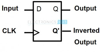
D flip – flop has two inputs , a clock (CLK) input and a data (D) input and two outputs; one is main output represented by Q and the other is complement of Q represented by Q’. The symbol of a D flip – flop is shown below.
Implementation
Working
1. When clk=0 and D=0
If the clock is low, both the output signals to the input stage of RS Latch are high regardless of the data input hence the output latch is unaffected and it stores the previous state
2.When clk=0 and D=1
Now if the Data input is changed to high, but the clock remains low, then again both the output signal to the input to RS latch are high. Hence regardless of the data input the output of the latch is not changed and it again retain its previous state.
3. When clk=1 and D=0
When clock is going through a positive transition ( low to high ) , the outputs of the input stage are responsible for set or reset operation of the final output and are dependent on data signal. If the data input is low, the output of the lower latch becomes low which resets the output to 0.
4. When clk=1 and D=1
When clock is high , the outputs of the input stage are responsible for set or reset operation of the final output and are dependent on data signal. If the data input is high, the output of the upper latch becomes low and thus sets the latch output to 1
Truth Table
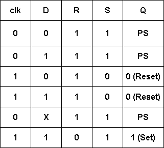
From the truth table we can conclude that any input given to data D doesnt matter or dont care when the clock is 0, and we get both the output as high to the input of RS latch. Hence regardless of the input given to the RS latch the output will always retain the previous state.
The circuit is closely related to the gated D latch as both the circuits convert the two D input states (0 and 1) to two input combinations (01 and 10) for the output SR latch by inverting the data input signal (both the circuits split the single D signal in two complementary S and R signals). The difference is that in the gated D latch simple NAND logical gates are used while in the positive-edge-triggered D flip-flop SR NAND latches are used for this purpose. The role of these latches is to "lock" the active output producing low voltage (a logical zero); thus the positive-edge-triggered D flip-flop can also be thought of as a gated D latch with latched input gates.
Timing diagram
Working Example
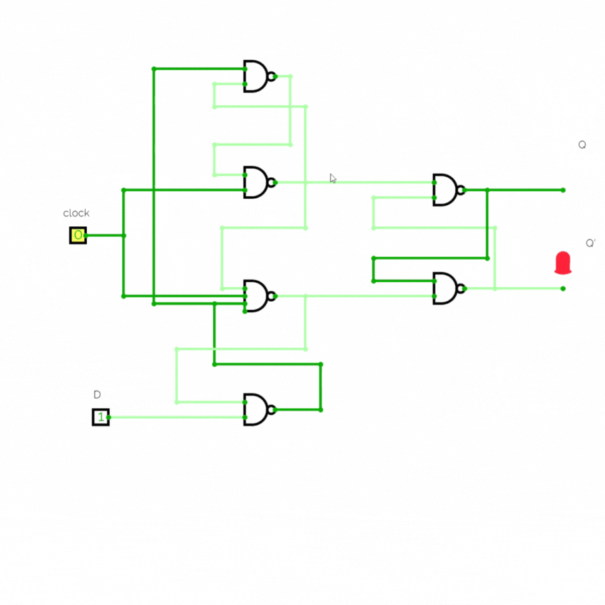
The light green wire shows that it is carrying one and dark green wire shows that it is carrying zero. It shows that output Q follows the input D only when the clock input changes from 0 to 1 (positive edge). Then even if the clock input remains 1 the output retains previous state does not change according to input. Hence this circuit acts as a positive edge triggered flip flop.