CMOS INVERTER - mbits-mirafra/digitalDesignCourse GitHub Wiki
What is CMOS Inverter?
The term CMOS stands for “complementary-symmetry metal–oxide–semiconductor” which is pronounced as “see mos”. CMOS is a type of MOSFET, where its fabrication process uses complementary & symmetrical P-type & N-type MOSFET pairs for logic functions. The main CMOS devices characteristics are consumption of low static power & high noise immunity. The inverter is accepted universally as the basic logic gate while performing a Boolean operation on a single i/p variable. A basic inverter circuit is used to accomplish a logic variable by complementing from A to A’. So, a CMOS inverter is a very simple circuit, designed with two opposite-polarity MOSFETs within a complementary way
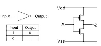
The CMOS inverter circuit diagram is shown above. The general CMOS inverter structure is the combination of both the PMOS & NMOS transistors where the pMOS is arranged at the top & nMOS is arranged at the bottom.
The connection of both the PMOS & NMOS transistors in the CMOS inverter can be done like this. The NMOS transistor is connected at the drain (D) & gate (G) terminals, a voltage supply (VDD) is connected at the source terminal of PMOS & a GND terminal is connected at the source terminal of NMOS. Input voltage (Vin) is connected to both the gate terminals of transistors & output voltage (Vout) is connected to the drain (D) terminals of the transistor.
It is very significant to observe that the CMOS device does not have any resistors, so it will be more power-efficient. Once the input voltage of CMOS changes between 0 to 5 volts, then both the transistors state will be changed accordingly
Working:
When the low input voltage is given to the CMOS inverter, then the PMOS transistor is switched ON whereas the NMOS transistor will switch OFF by allowing the flow of electrons throughout the gate terminal & generating high logic output voltage.
Similarly, when the high input voltage is given to the CMOS inverter then, the PMOS transistor is switched OFF whereas the NMOS transistor will be switched ON avoiding as many electrons from attaining the output voltage & generating low logic output voltage.
Let's consider a different scenario! What happens if two different inputs are given to PMOS and NMOS? What happens when both PMOS and NMOS turns ON? What might be the output?

Check out this video!!!
Yes, as you can see its neither 1 nor 0. That means its invalid condition.