board howto - andreika-git/hellen-one GitHub Wiki
How to create a board?

The board creation process consists of the following steps:
- Create a project for your [frame] using your favorite EDA software (Kicad, Altium CircuitMaker/Designer).
- Export your frame into a separate folder (eg. "gerber"): gerber and NC drill files, schematics in PDF, BOM and CPL in csv, 3D component models in VRML (WRL). Please refer to How to export a frame from Kicad for more info
- follow https://github.com/andreika-git/hellen-one/blob/master/readme.md
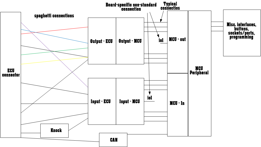
Frame flowgraph
It is recommended to place main connector on the left side of the schematics for best readability.
Common Board usability features
- Main connector pin numbers silkscreen (usually on the back of the board)
- Main connector per pin function silkscreen where we have space
- Board name, revision and relevant URL on both top and back silk
- DFU and Reset buttons
- LED-convention
- GND 3v, 5v, 12v test pads on front of PCB
- GND test pad on back side of PCB
- Proto area with enough interesting vias wired: GND, 3v, 5v and a few GPIO
- Floating/disconnected proto area with vias connected in pairs or groups of three
- Backup power for real time clock - battery holder or else
- White silkscreen notes area