v1.1 1. Main Board 1 - alanbjohnston/CubeSatSim GitHub Wiki
CubeSatSim Main Board Assembly Part 1
NOTE: These are not the steps for the latest CubeSatSim version, but for v1.0 and v1.1 of the hardware.
In these steps, you will start building your Main board.
To do this, you will need the parts in the v1.1 BOM https://docs.google.com/spreadsheets/d/1y94Ut4WlnfJ7ZC4sU9S5768G5_BMU9aPUGnHsb_djTI/edit?usp=sharing and these tools:
- Safety glasses (to protect eyes while soldering or trimming leads)
- Soldering iron and solder (I use lead-free solder, but leaded solder is easier to work with)
- Needle nose pliers (to bend leads and hold parts)
- Side cutters (to trim leads)
Other tools that are helpful:
- Blue mounting putty (to hold components in place while soldering)
Video
Here is a video showing this assembly step: https://youtu.be/yIlTwG-H96Q
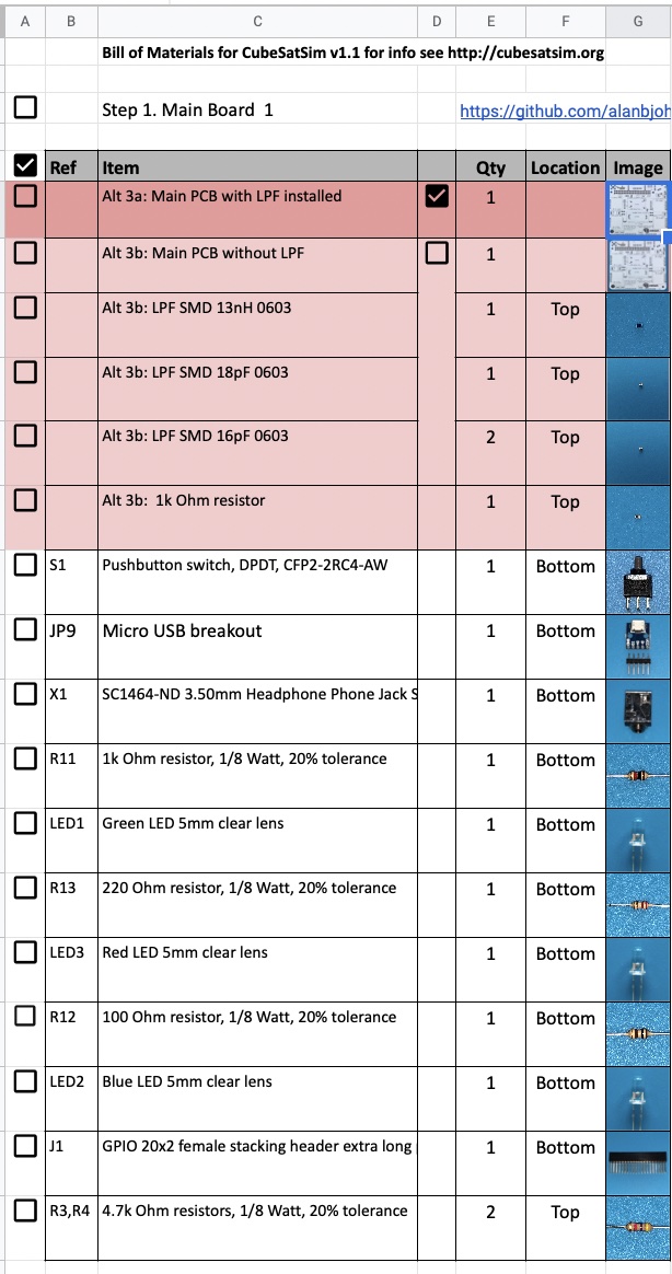
Checklist
The BOM has a sheet "By Steps" which lists the parts needed for each step in order. http://cubesatsim.org/bom If you have a Google account, you can make a copy of this spreadsheet ("File" then "Make a Copy") and check off each part as you install it.
For example, here is the checklist for this step:
Main Board Instructions
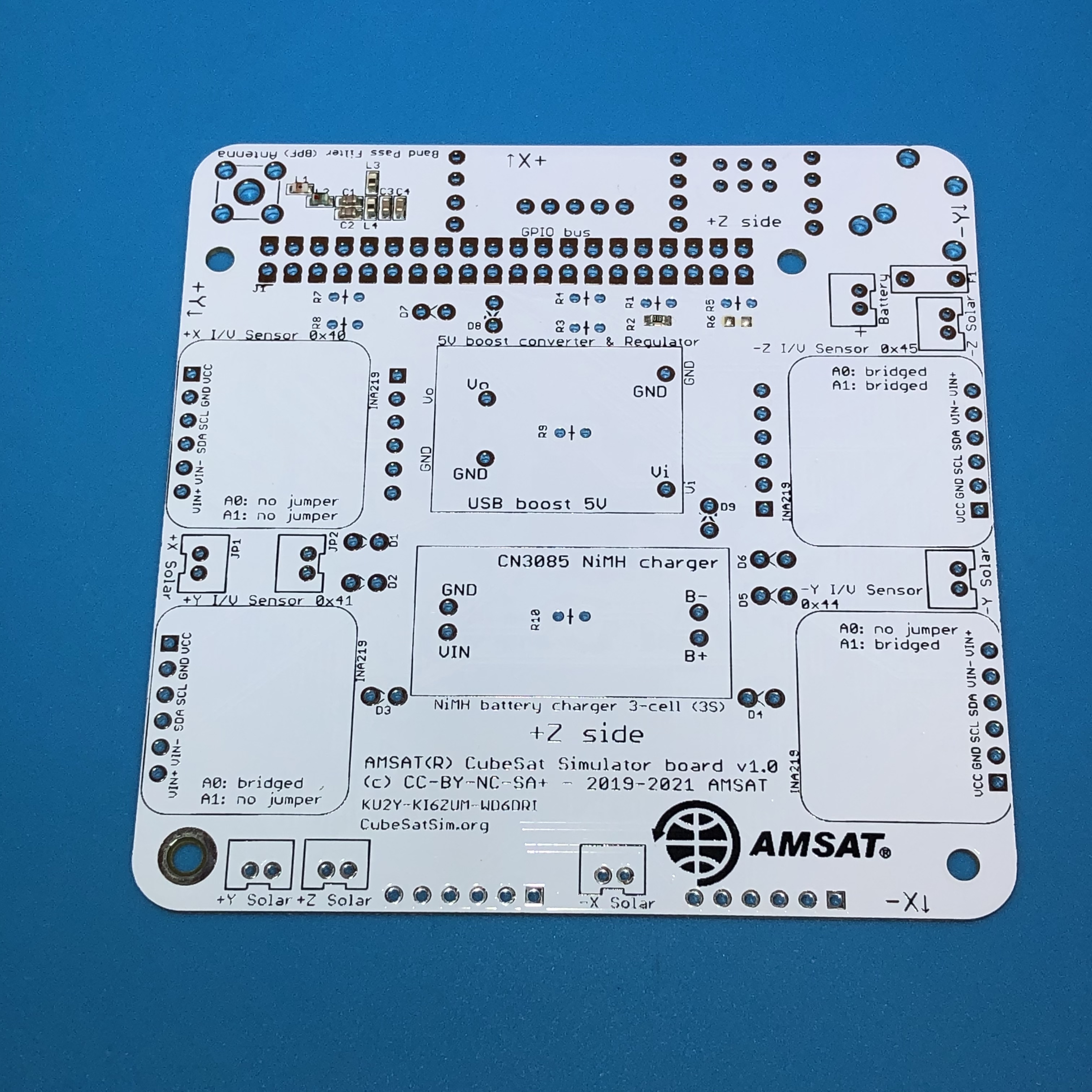
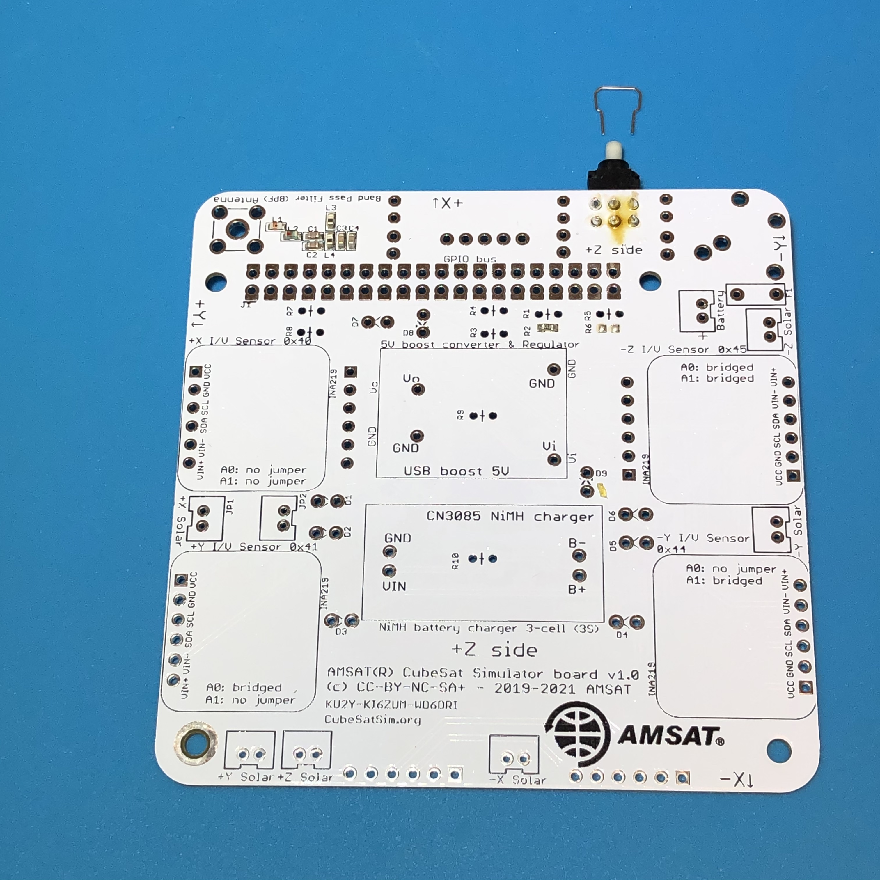
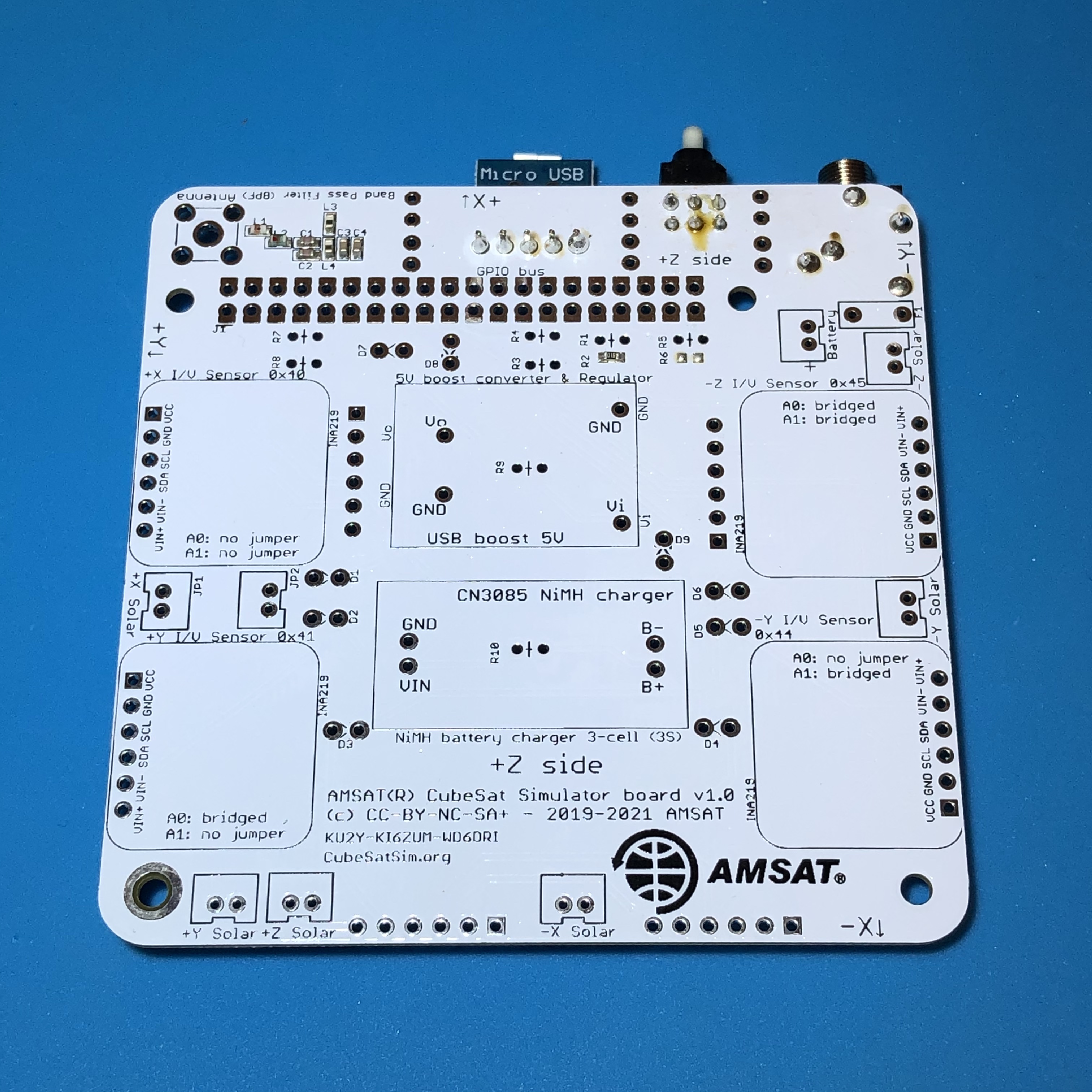
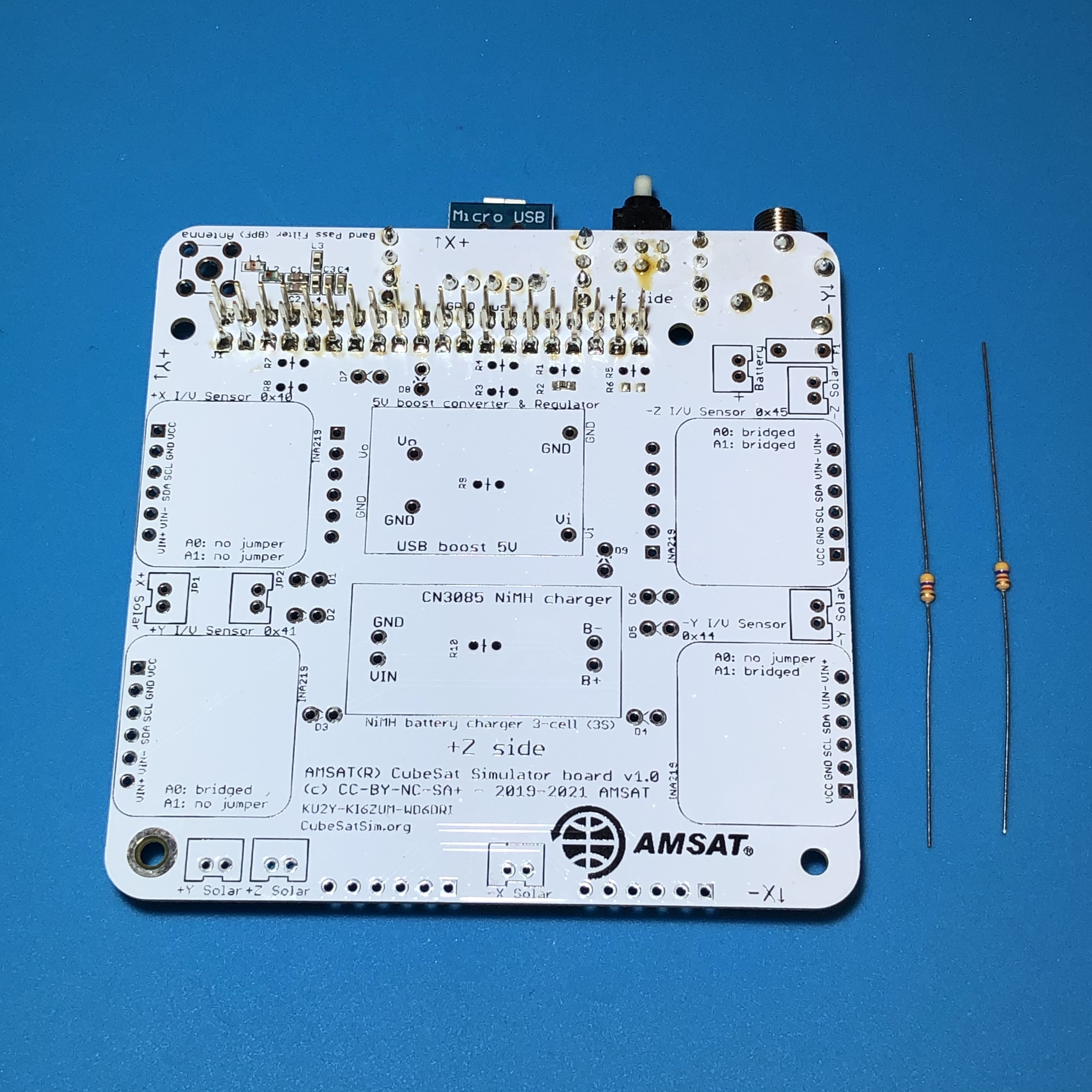
The PCB has components on both sides. This is the top of the PCB, with the AMSAT logo.
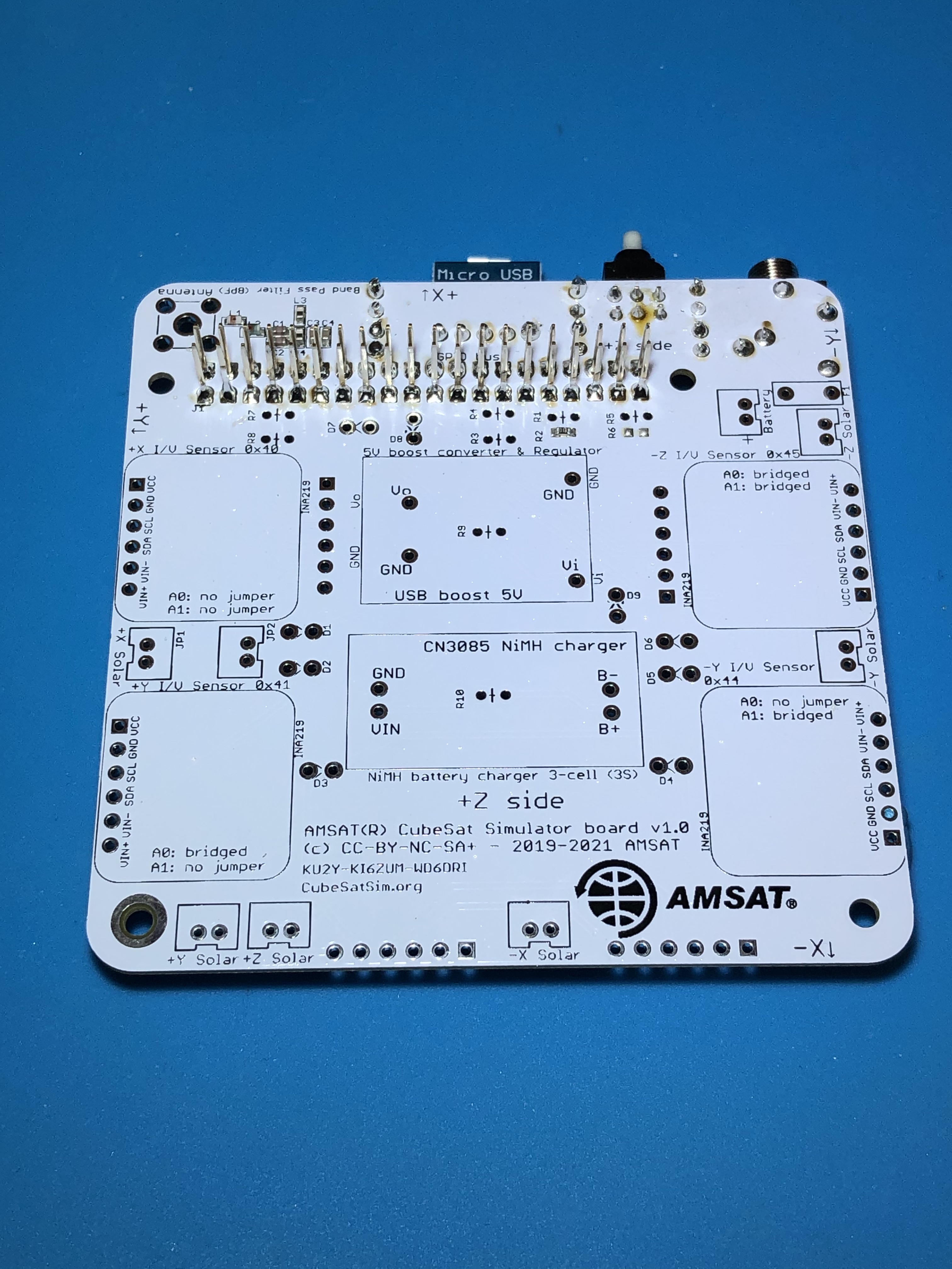
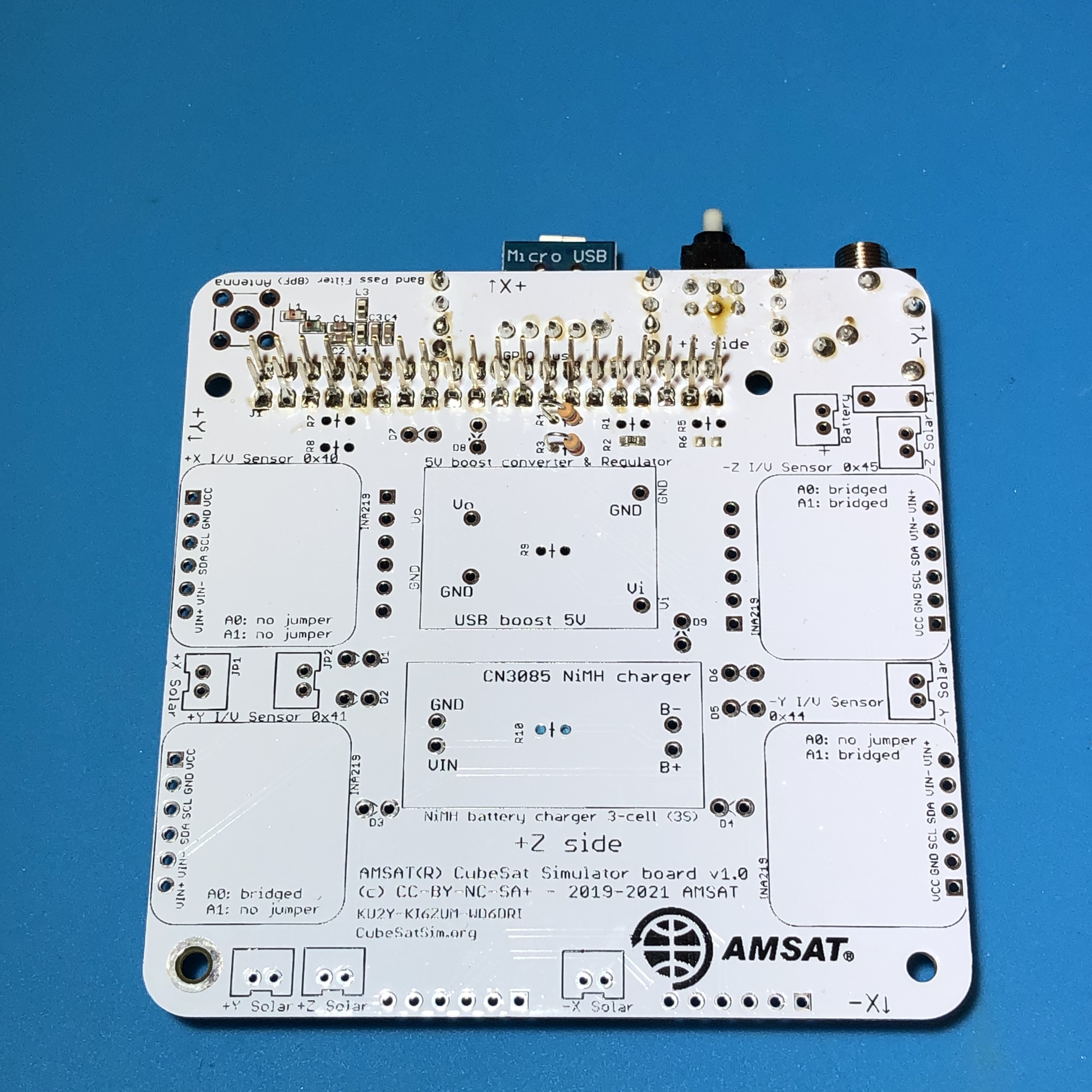
This is the bottom of the PCB.
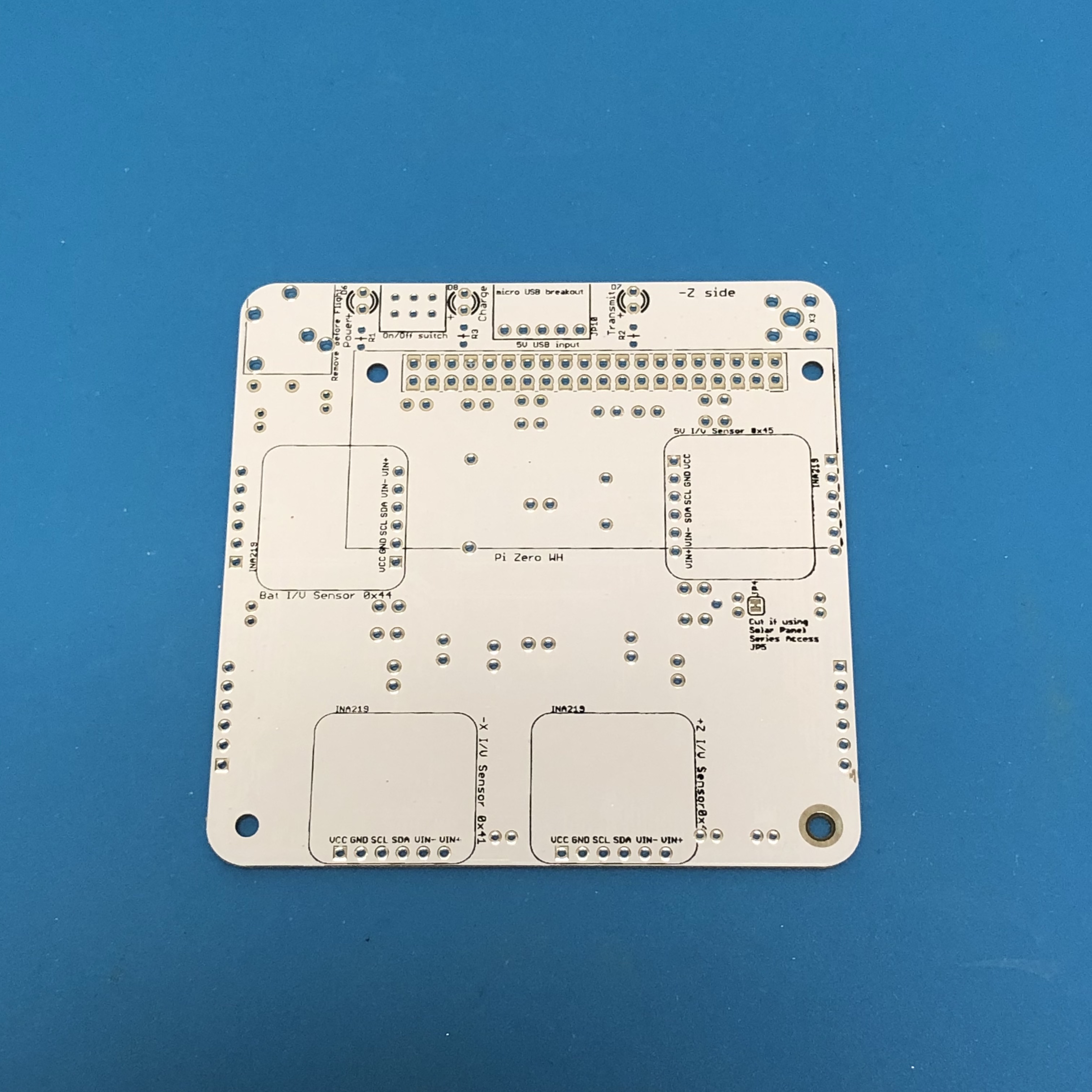
The silkscreen outline markings indicating which side to mount the parts.
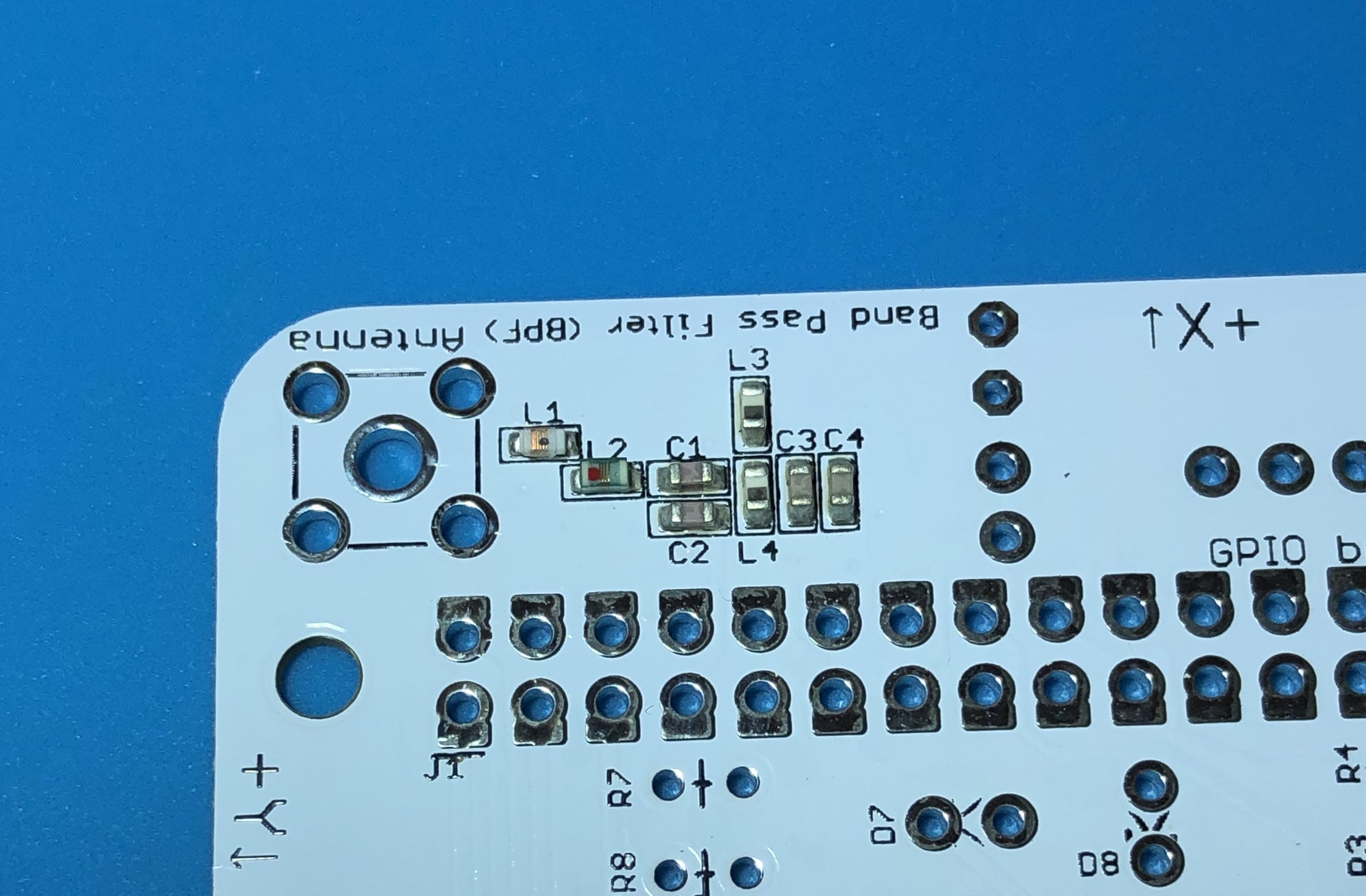
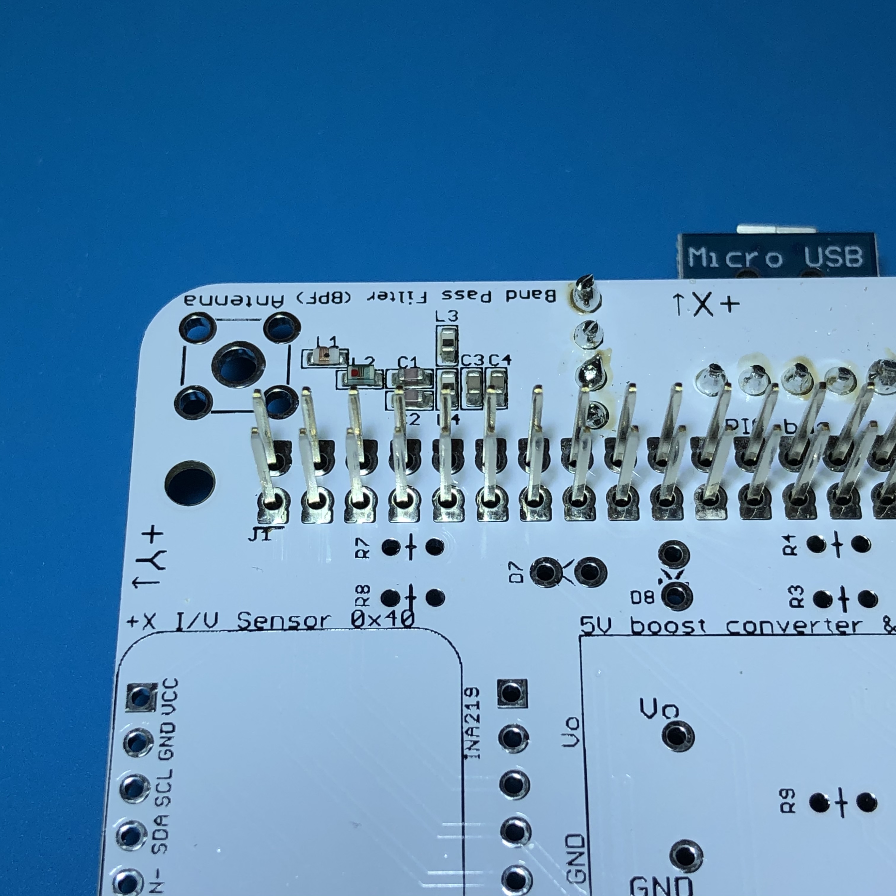
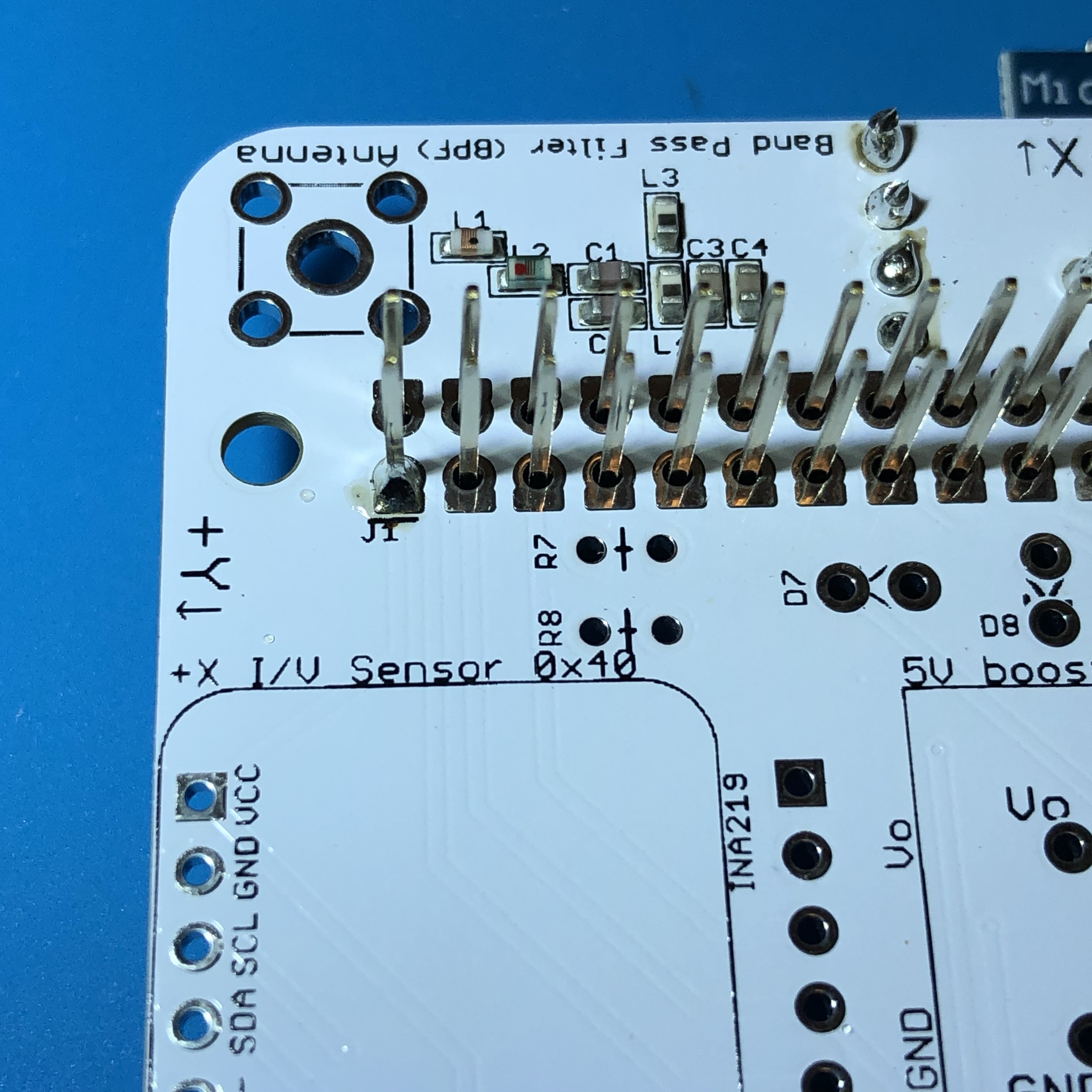
Before any components are soldered onto the board, the Surface Mount Device (SMD) components for the Band-Pass Filter (BPF) must be installed, if they aren't already soldered on. The purpose of the BPF is to filter out all the undesirable radio frequency (RF) emissions besides the ones at 434.9 MHz UHF (i.e, harmonics, sub-harmonics, and spurs). Here is a closeup of the SMD components after they have been mounted:
If you don't have the ability to do SMD soldering, you can instead use an external Band-Pass Filter with SMA connectors. For example, this BPF works quite well https://www.amazon.com/gp/product/B07R8Y1PM4/
The instructions for the tape measure monopole or dipole are in the Board Stack instructions.
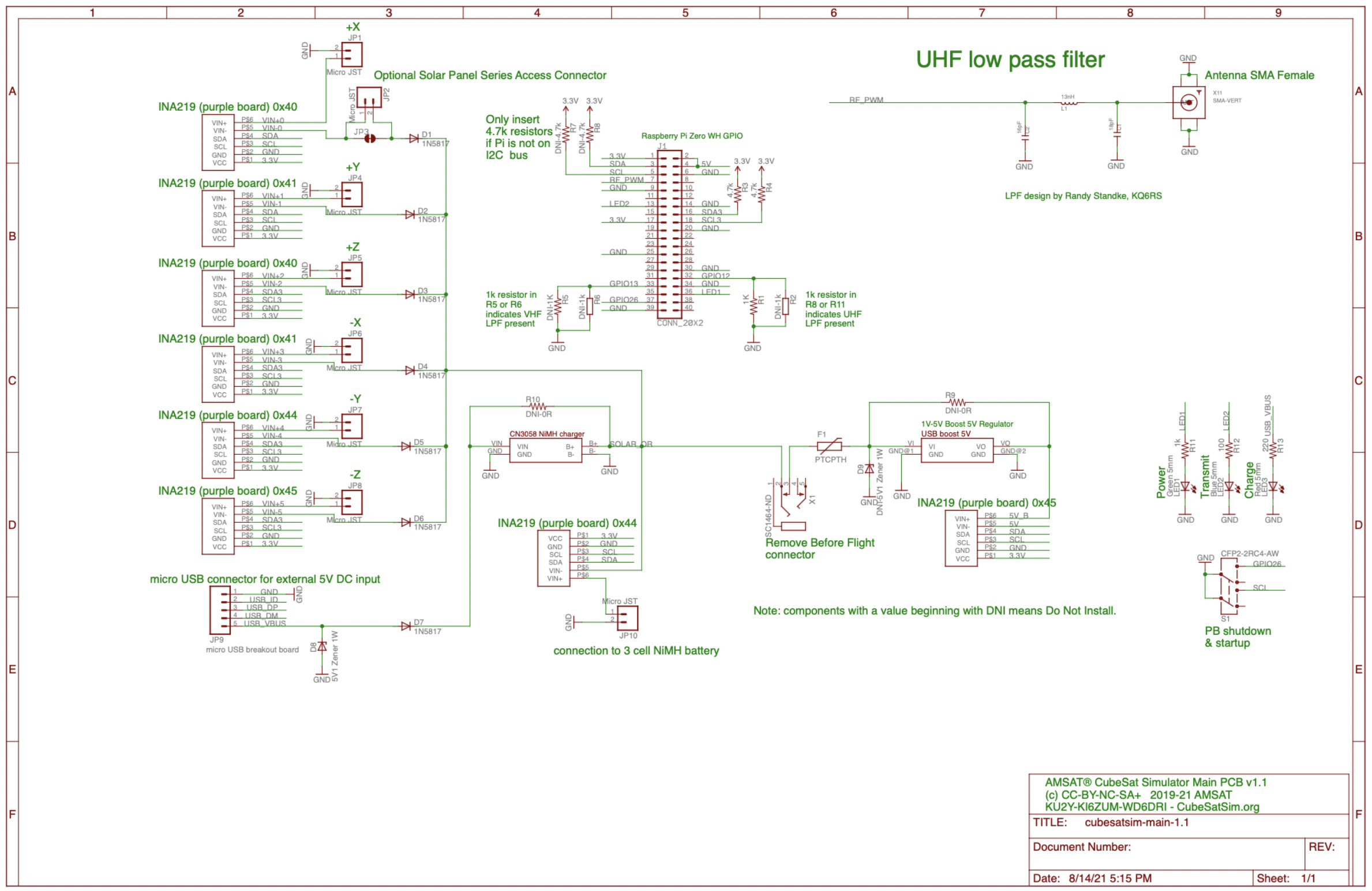
Here's the schematic for the Main board for reference:
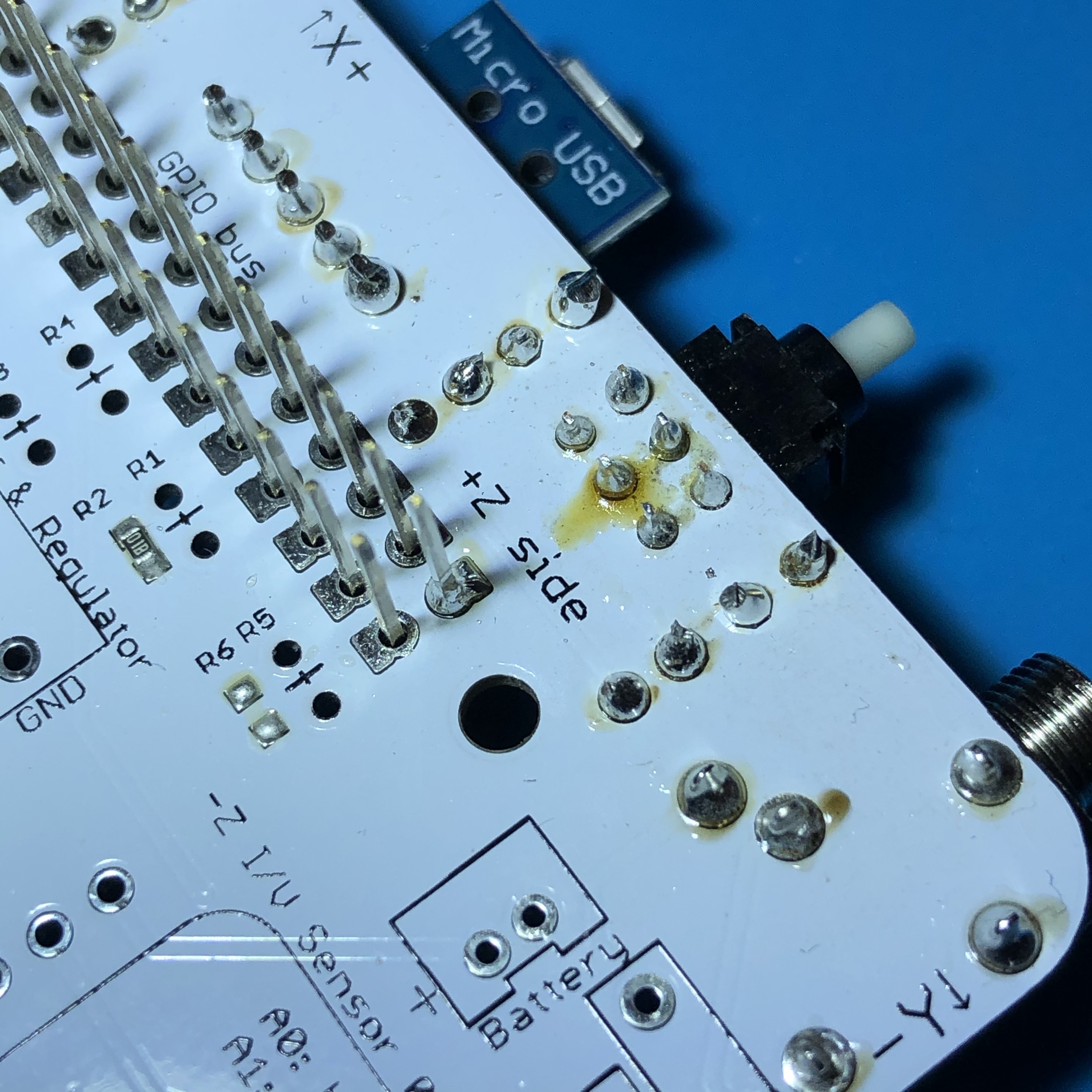
First, we will start soldering the components on the bottom of the PCB. The printed outlines on the board indicate that a part should be installed on that side, with the pins soldered on the other side. For components with multiple pins, solder just one pin first, then flip the board over and verify that it is flush with the board and straight. It is a lot easier to fix this with only one pin soldered than with multiple pins. It is also one last check to make sure you are mounting it on the right side. For some parts, such as resistors or diodes, mounting on the wrong side won't matter. For others, such as LEDs and switches and connectors, mounting on the wrong side will make it more difficult to mount the solar panels. But other parts, such as a the stacking GPIO headers or the INA219 boards, must be mounted on the correct side, so double check carefully.
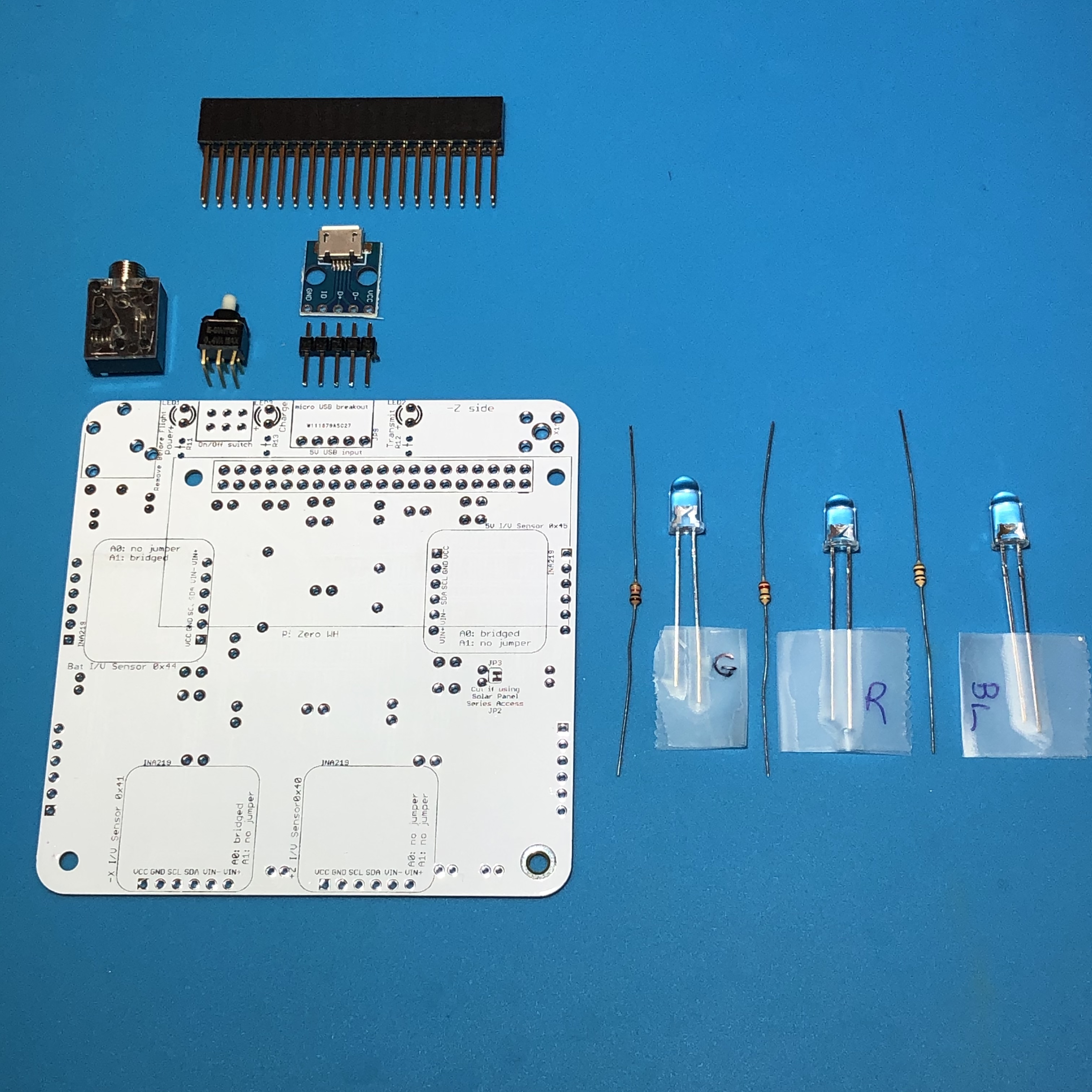
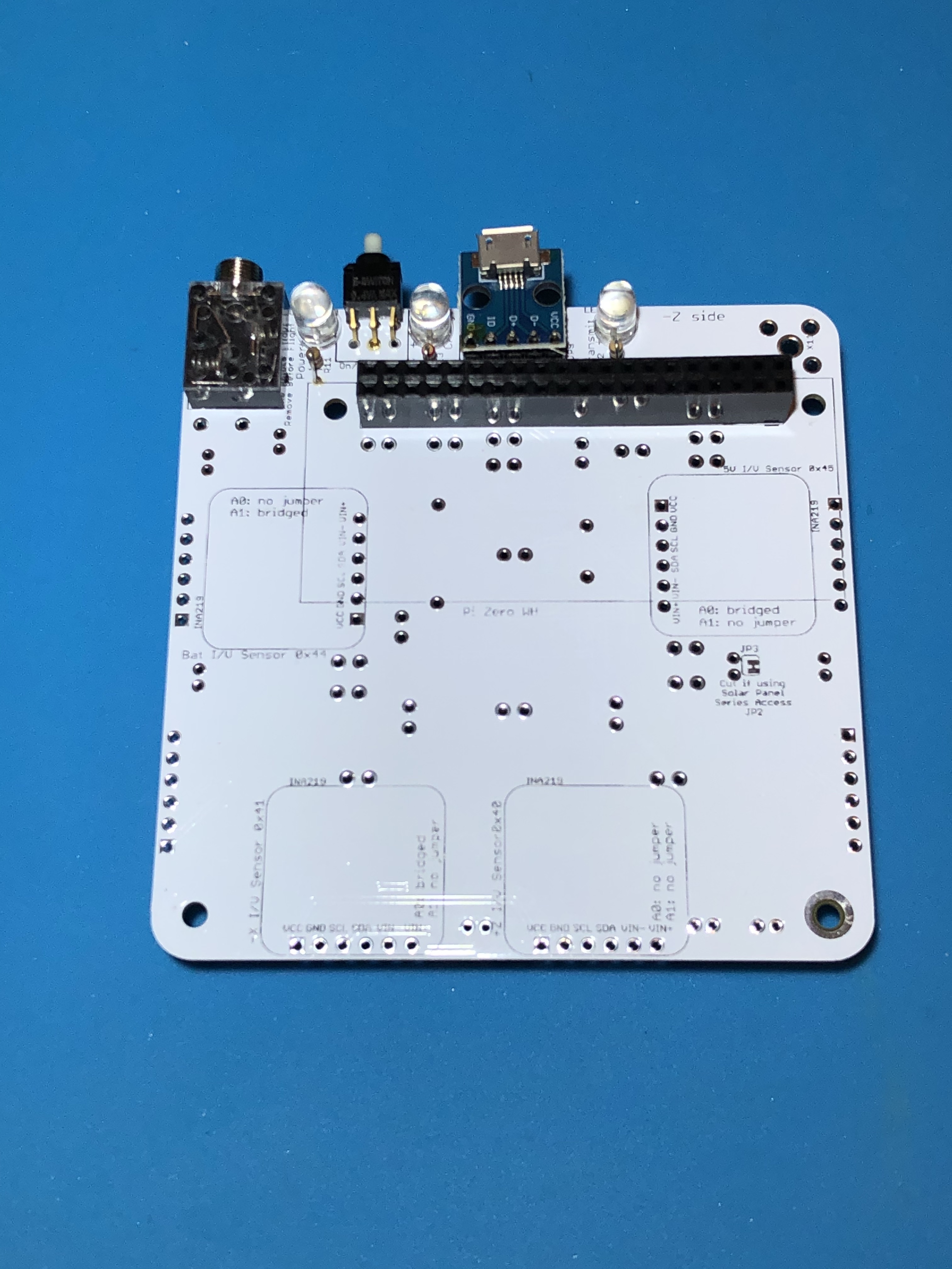
This photo shows the initial set of parts to be mounted on the bottom of the PCB and the bottom PCB view:
Start with the push button switch S1. This momentary push button switch is used to power up the CubeSatSim when it is off, or to change modes or shutdown when it is running. Note that to allow the button to be pressed when mounted in the frame with solar panels, the switch hangs over the edge. An extra mounting clip doesn't touch the board and can be removed, as shown here:
Next, is the micro USB breakout board, which provides 5V DC to charge the batteries. The breakout board is mounted on a 1x5 pin header that came with the board. You first solder the micro USB board to the 1x5 pin header. Then on the other side of the PCB, the pin header is soldered to the board. Using blue mounting putty, you can hold the board in place, and solder it as shown here:
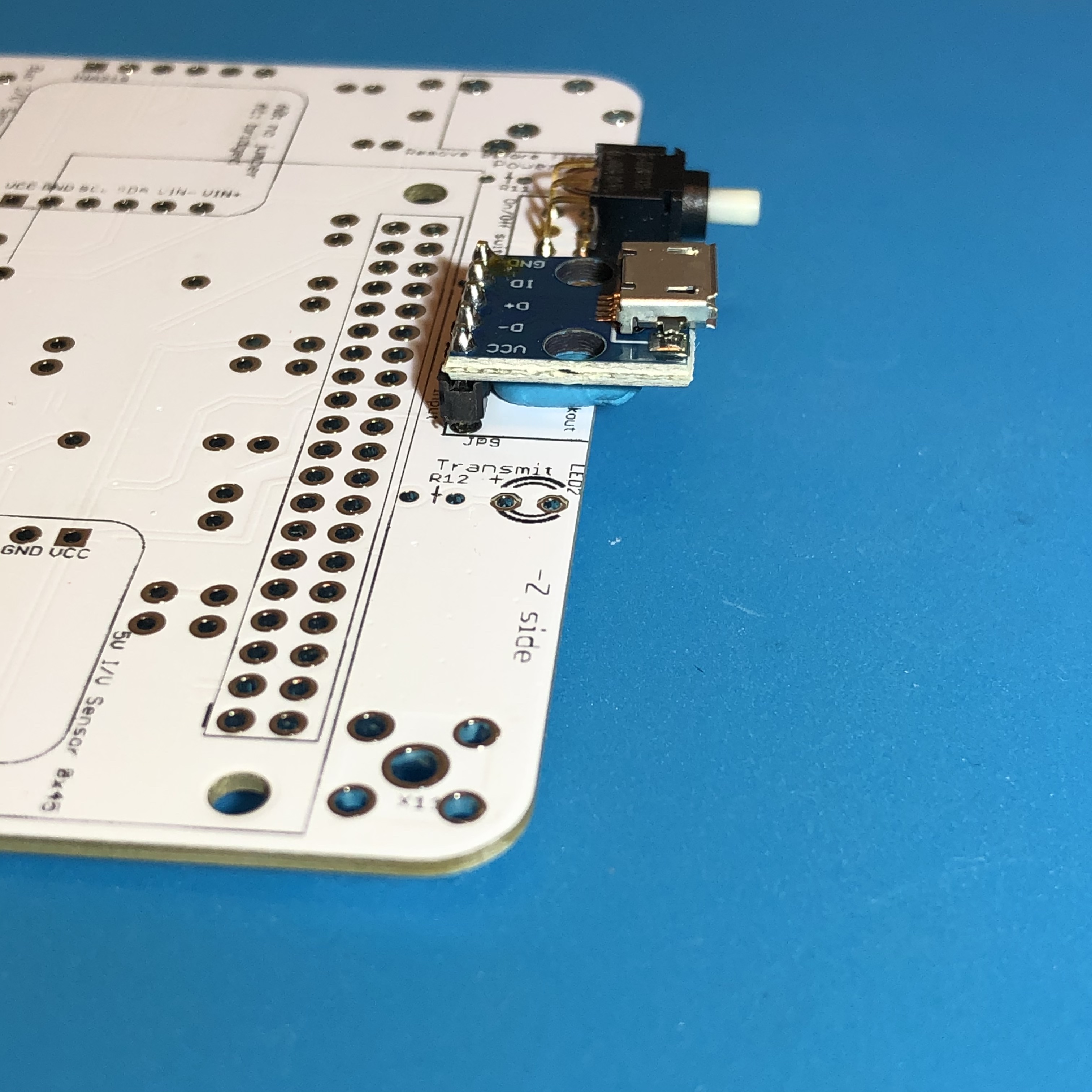
Another way to easily solder this straight is to use the STEM Payload board along with a 1x6 pin header from one of the INA219 boards as shown here, allowing the 1x5 pin header to be soldered to the breakout board:
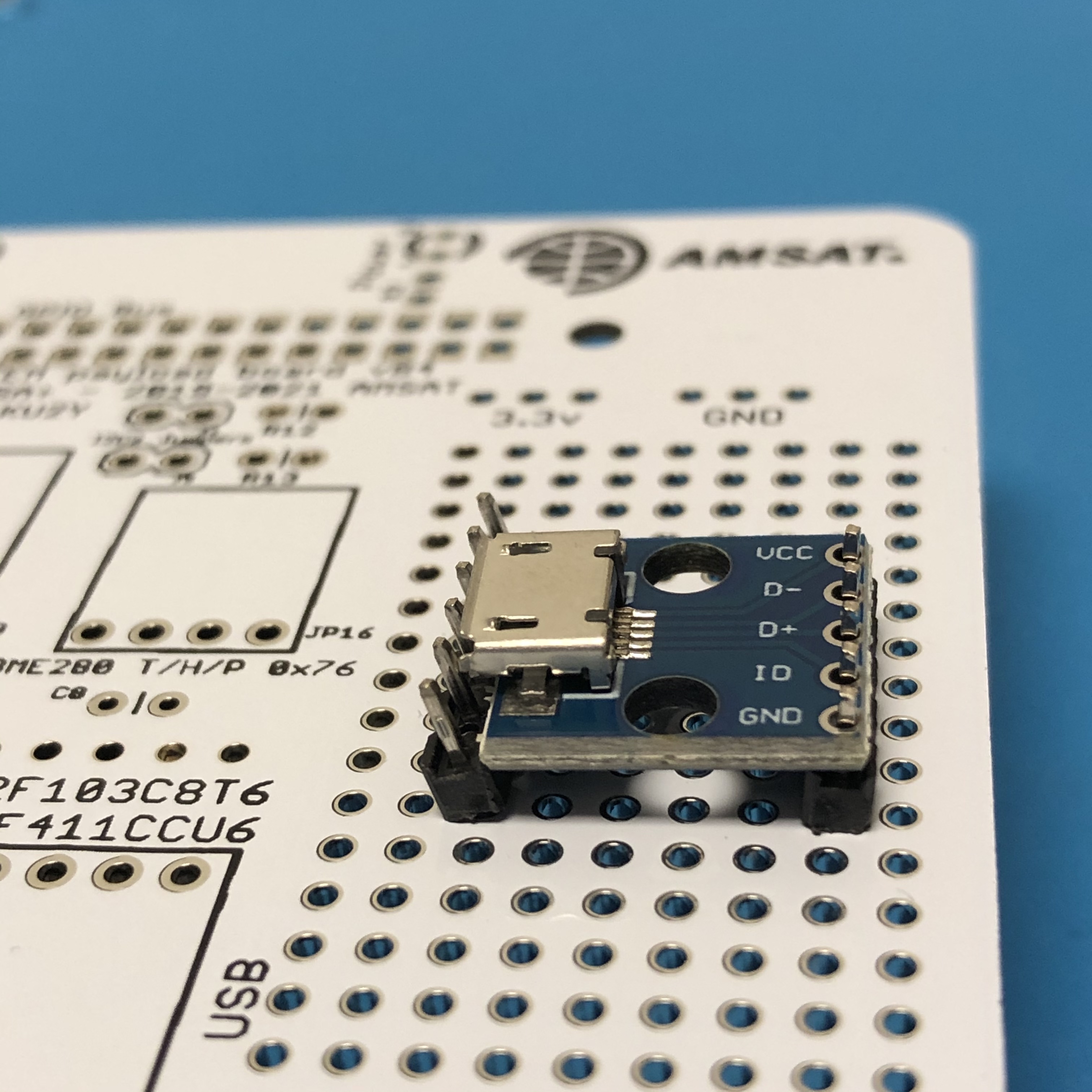
Next, trim the excess length of the 1x5 pin headers with the side cutters. Be sure to wear your safety glasses and watch out for the flying off-cuts. However, you can leave them without any problems. The same is true for the purple INA219 boards later on.
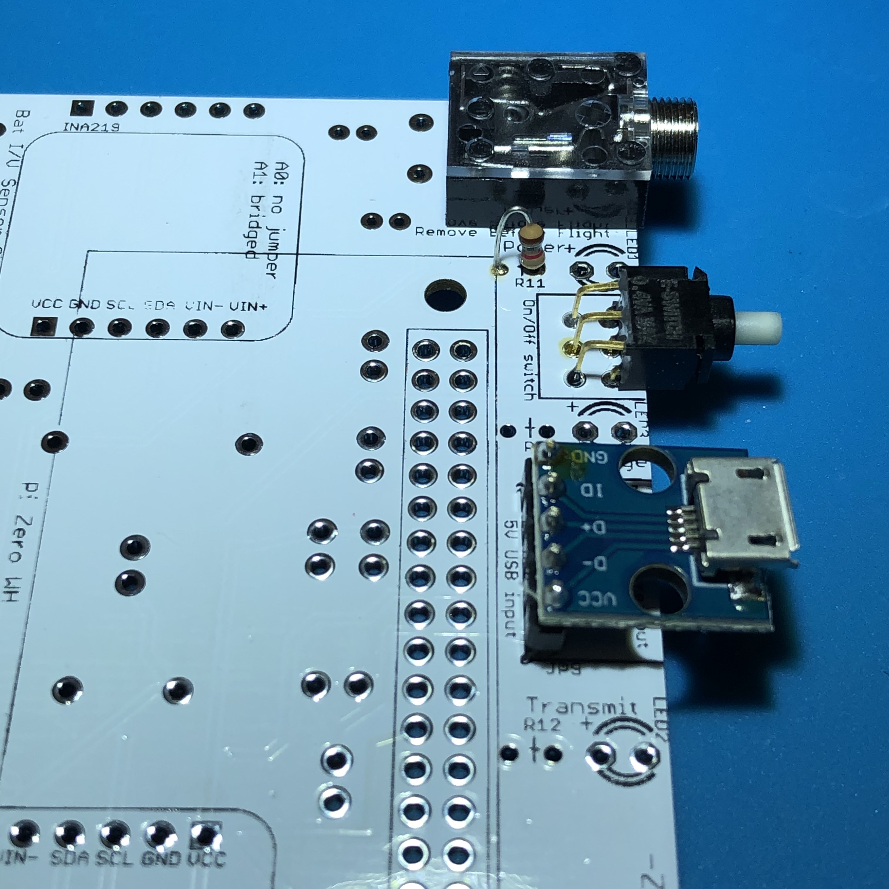
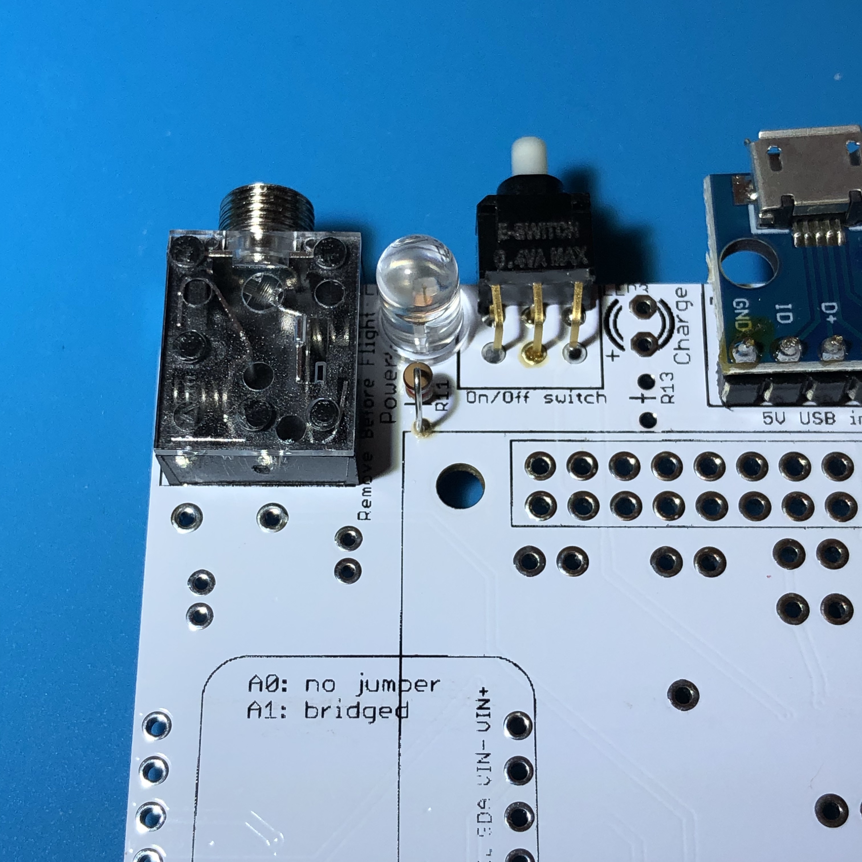
Then, solder X1 the 3.5mm audio jack, which has a contact switch (you can see the contacts with the springs if you look through the clear cover) for our Remove Before Flight (RBF) switch. This switch disconnects 5V power from the Pi forcing the CubeSatSim into a powered down mode for transporting or storage, or, on a real CubeSat, prior to launch.
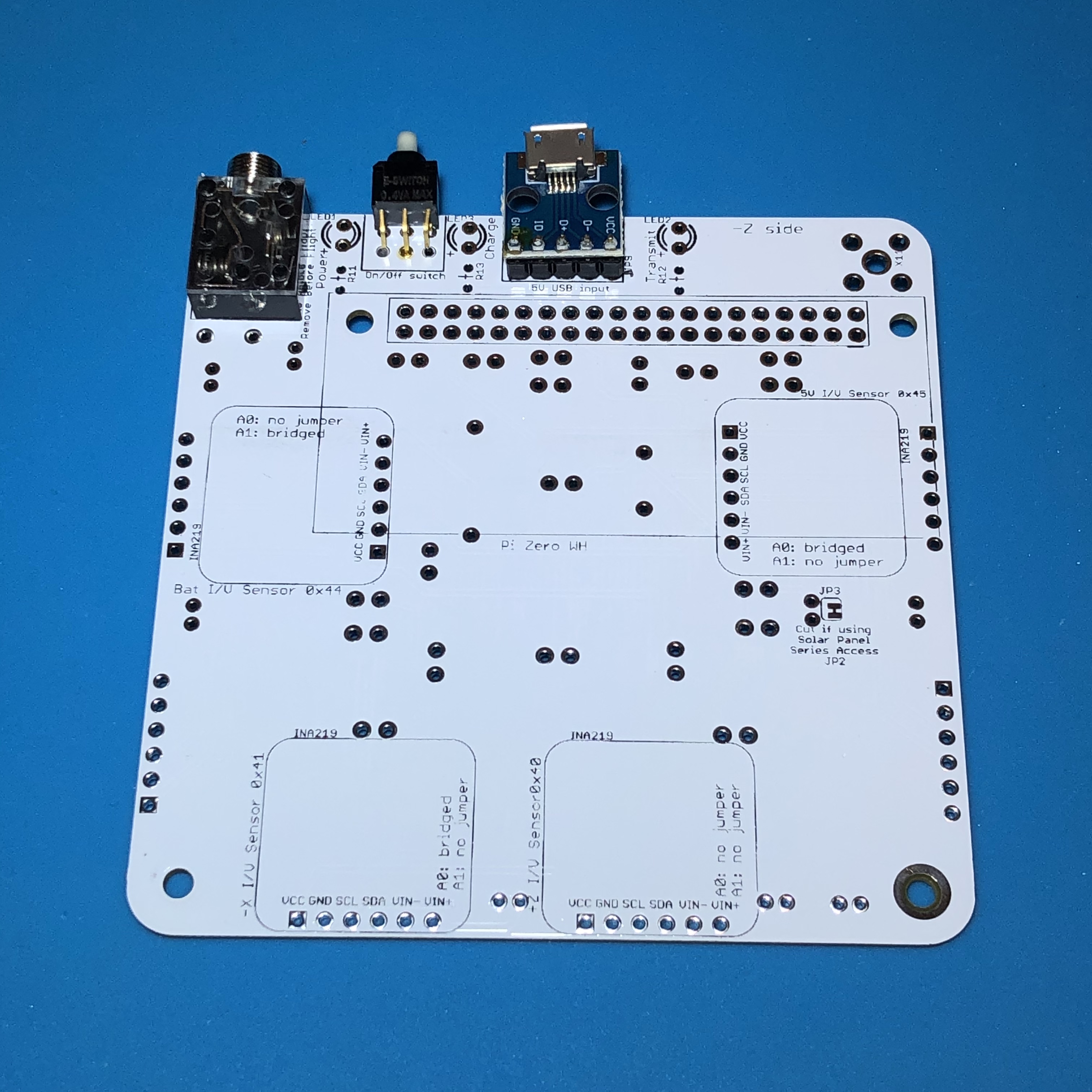
Here's how it looks on the top of the PCB with the three components mounted:
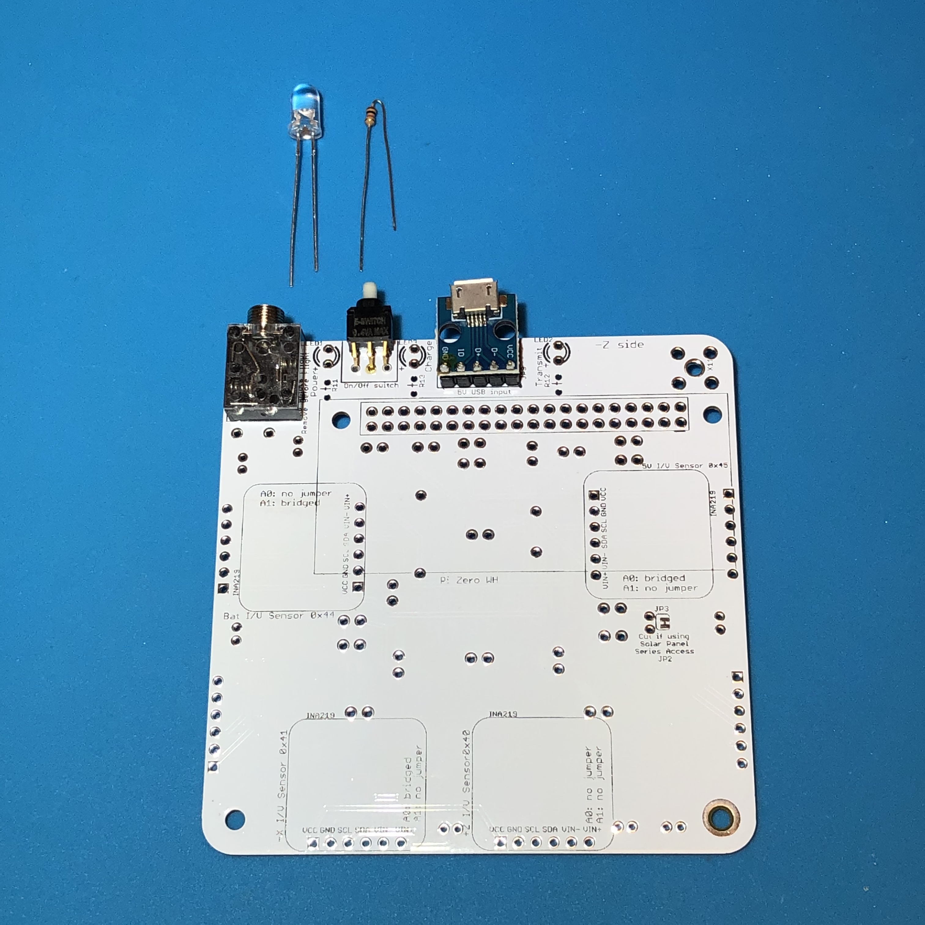
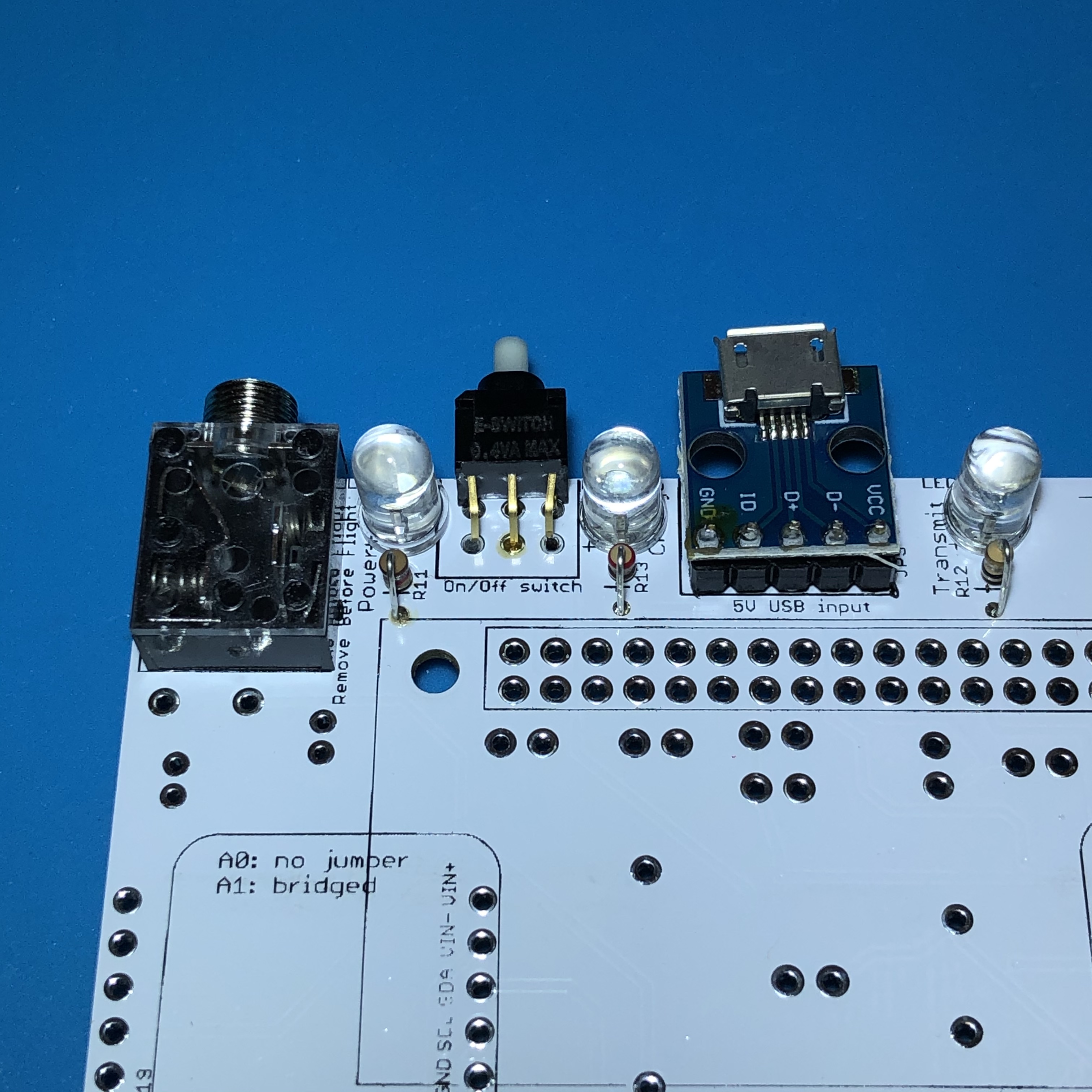
Next we will solder the resistors R11, R12, and R13, and the three LEDs LED1, LED2, and LED3. If you are using clear lens LEDs, be careful not to mix up the colors! If you are not sure, test them with 3.3V and resistor R11 to see what color it is. LEDs need to be installed with the correct polarity (one lead is + polarity and the other lead is - polarity) or it will not illuminate. The longer leg on the LED is the '+' lead and should be away from the edge of the PCB. Also, if you look at the LED lens from the top, it is circular but there is a flat side that marks the '-' side. So the flat side of the LED should be towards the edge of the PCB.
To save space on the PCB, all resistors and diodes are mounted vertically, so you have to bend over one of the leads to get a U-shape, allowing it to be inserted into the two closely-spaced holes. This photo shows the green Power LED1 and 1k Ohm resistor R11 (the color bands on the resistor are brown black red - see https://en.wikipedia.org/wiki/Electronic_color_code for details) which are about to be inserted between the RBF switch and the micro USB board. Note the longer plus lead of the LED is on the left here:
Here's how the resistor looks when it is installed:
Here is the resistor and LED installed:
After you have soldered the resistor and LED, trim the excess leads with your side cutters.
Next, install the red Charge LED3 and 220 Ohm resistor R13 (color bands red red brown), then the blue Transmit LED2 and 100 Ohm resistor R12 (color bands brown black brown):
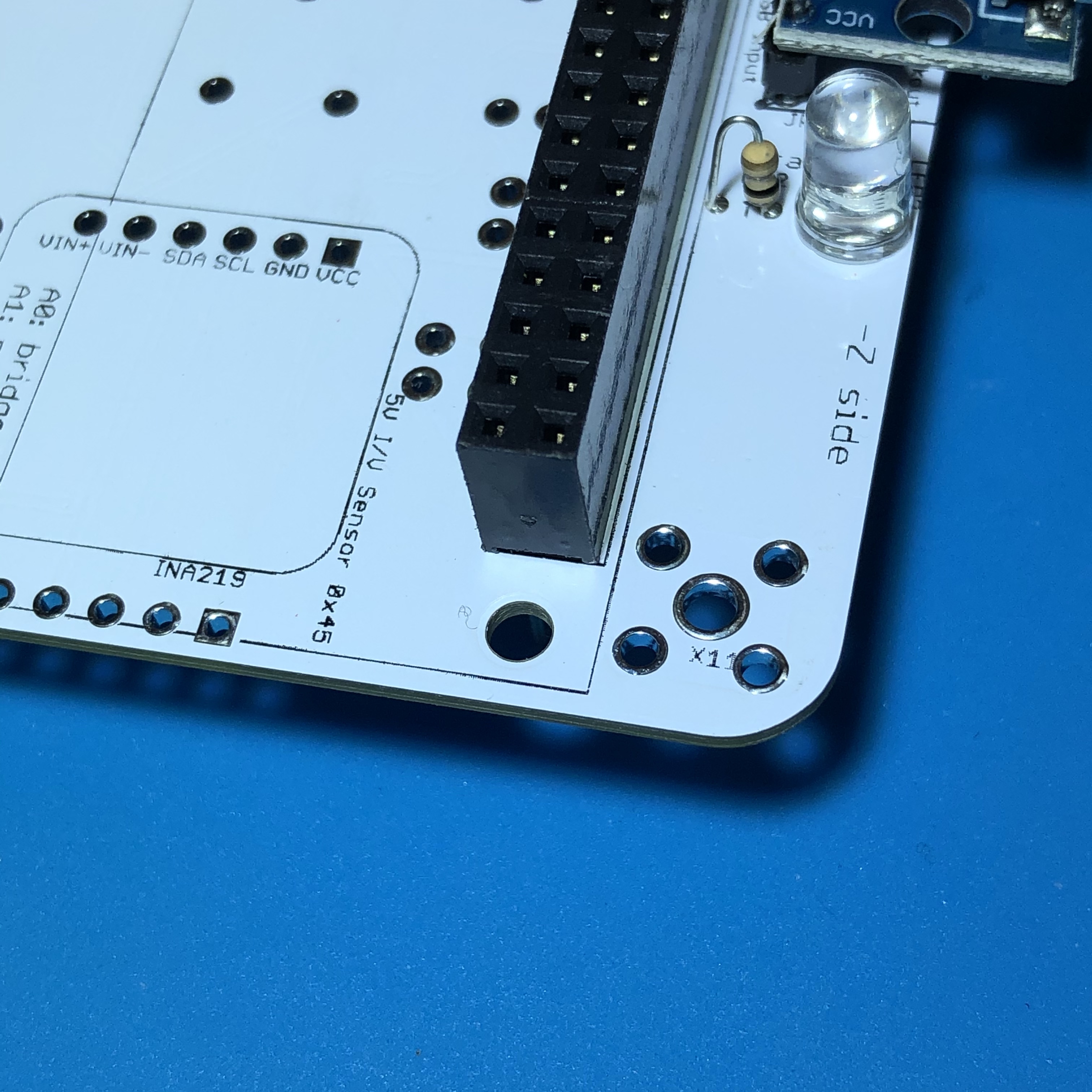
The final step is to install the stacking GPIO header J1. We use the Raspberry Pi GPIO as our spacecraft bus, and it connects the Pi and the three boards together. We will insert the stacking GPIO header on the bottom of the PCB and solder the pins on the top of the PCB.
IMPORTANT: Do not trim the leads on this stacking header, since the long leads are needed to plug the next board on top! It is also important that you don't get excess solder on the top of the GPIO pins or it might be hard to plug then next board in.
Here's how the stacking GPIO header looks on the top of the PCB ready for soldering. To make it easier solder, the PCB has enlarged pads making it easier to apply heat.
If you place your soldering iron on this pad touching the pin, you should be able to get heat to both the pin and pad to solder it.
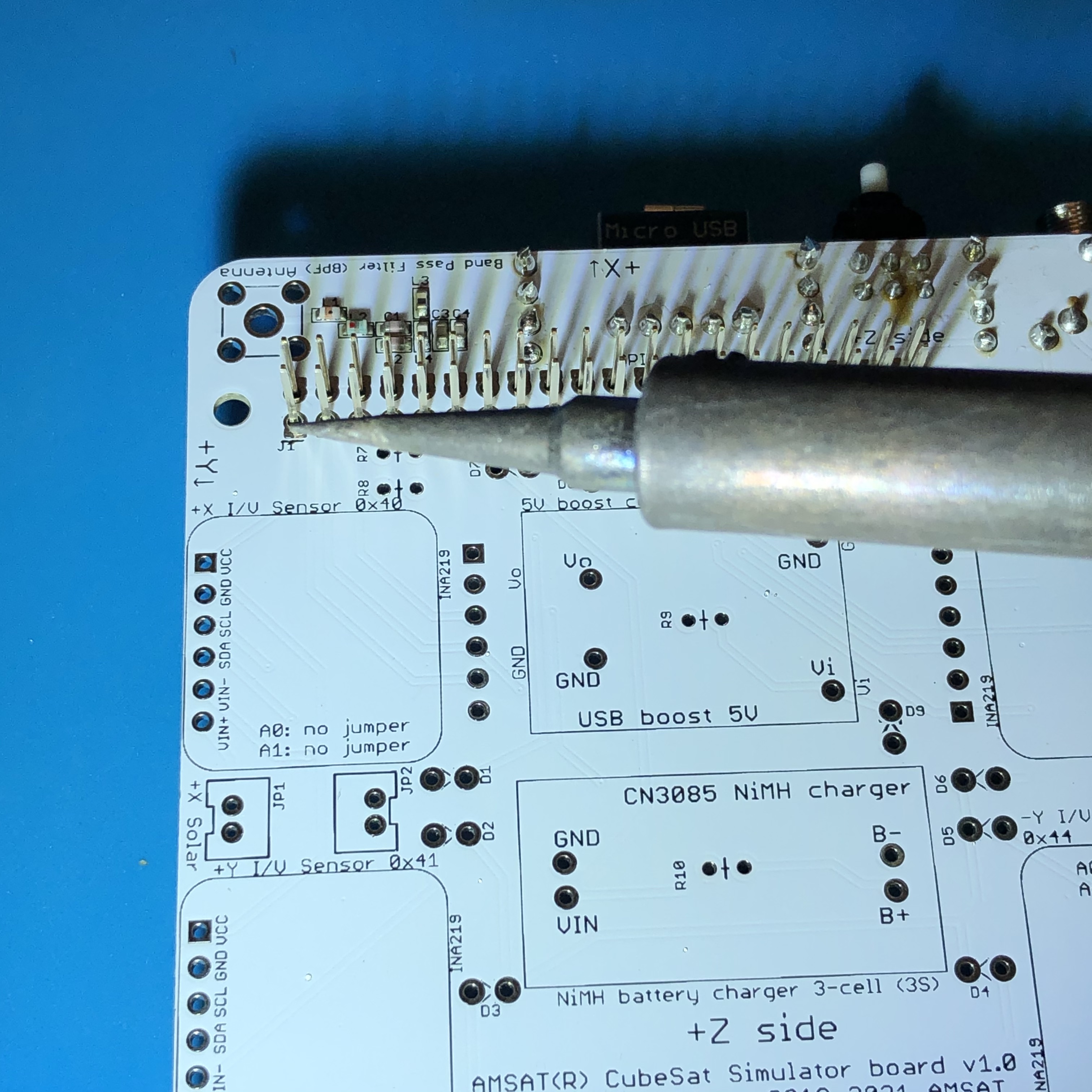
Solder only one pin on each diagonal corner of the connector, then double check that it is pressed down all the way and straight before going back and soldering the other pins.
Here's how it should look on the bottom of the PCB:
If it looks good, go ahead and solder the rest of the pins. Here's how it looks on the top of the PCB with one row soldered in:
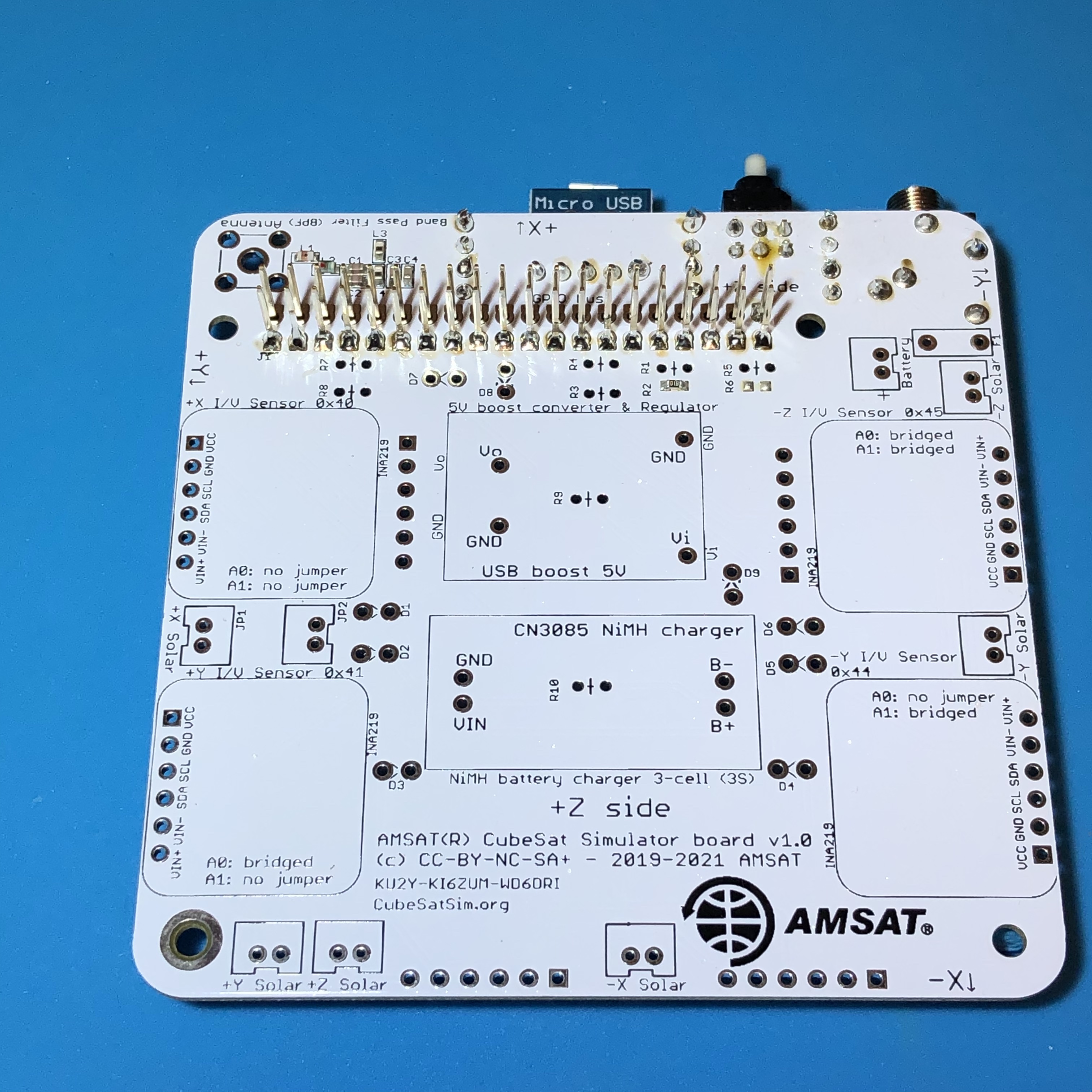
Here's how it looks on the top of the PCB after soldering, ready to stack the other boards on top:
Here's how it looks on the bottom of the PCB, ready to plug the Pi Zero WH into the female connector:
Next we install the 4.7k resistors R3 and R4 (color bands yellow violet red). They are pull-up resistors on the second I2C bus (pronounced "I squared C bus" which stands for Inter-Integrated Circuit bus) on the Raspberry Pi. Two of these buses are used by the Pi to read the INA219 current and voltage sensor boards we will install in the next section.
R3 and R4 are the first components we mount on the top of the PCB, so you will solder the leads on the bottom of the PCB:
Like all the resistors on the board, they are installed vertically:
Note that if your PCB had the SMD Band-Pass Filter components installed, there will be a 1k SMD resistor in R2 (labeled "102" for 10 * 10^2 or 1000 Ohms) as shown here:
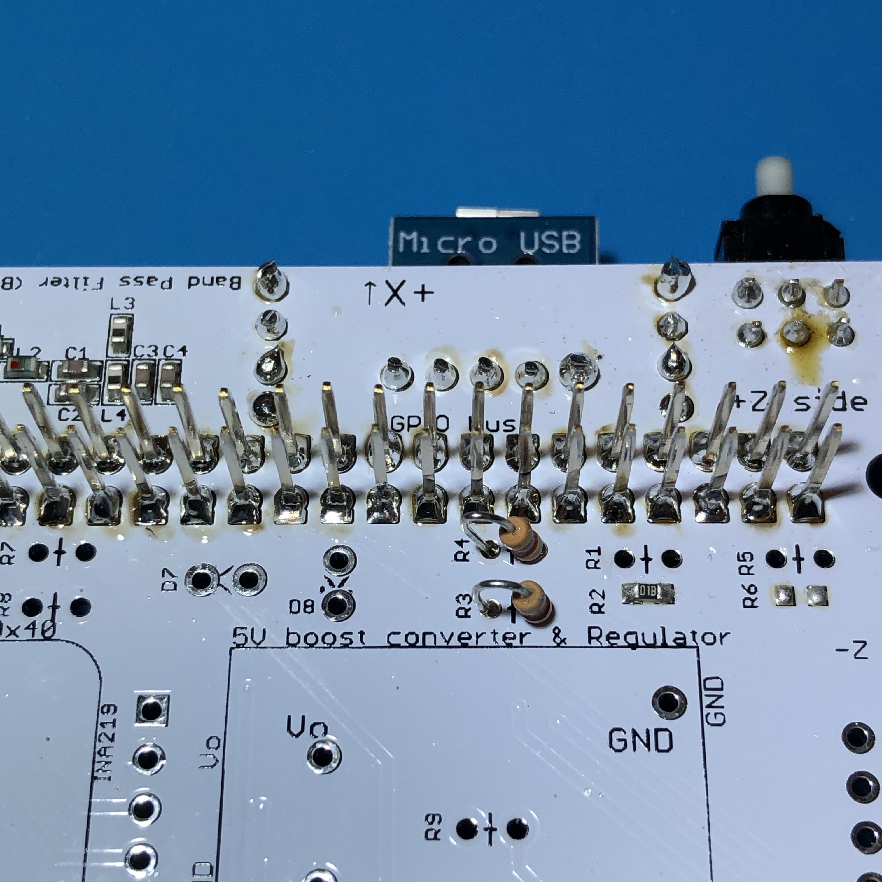
If there is no resistor in R2, you should install a 1k resistor (color band brown black red) in R1 next to it. This resistor is connected to a GPIO input on the Raspberry Pi and is used to sense if there is a Band-Pass Filter installed. If the filter isn't installed, the software will only transmit the CW callsign and will not send telemetry, as the signal might interfere with other stations. R1 or R2 are used to indicate the usual UHF Band-Pass Filter. If you installed a VHF Band-Pass Filter, you would install a resistor in R5 or R6.
You have completed Part 1 of building the Main board.
Next step is to Install the Software.