Solar Power Board Assembly Instructions - alanbjohnston/CubeSatSim GitHub Wiki
Solar Power Board Assembly Instructions
Steps:
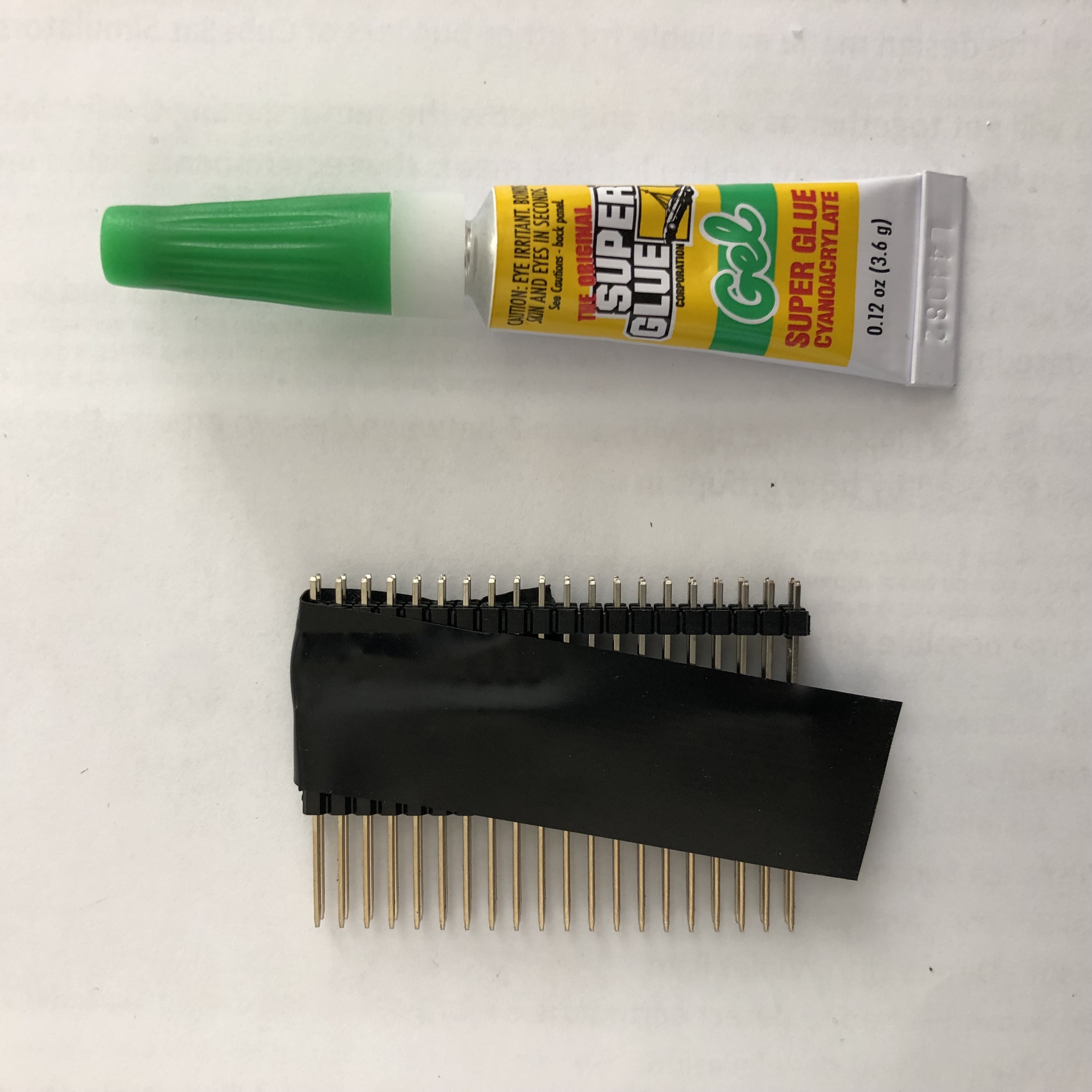
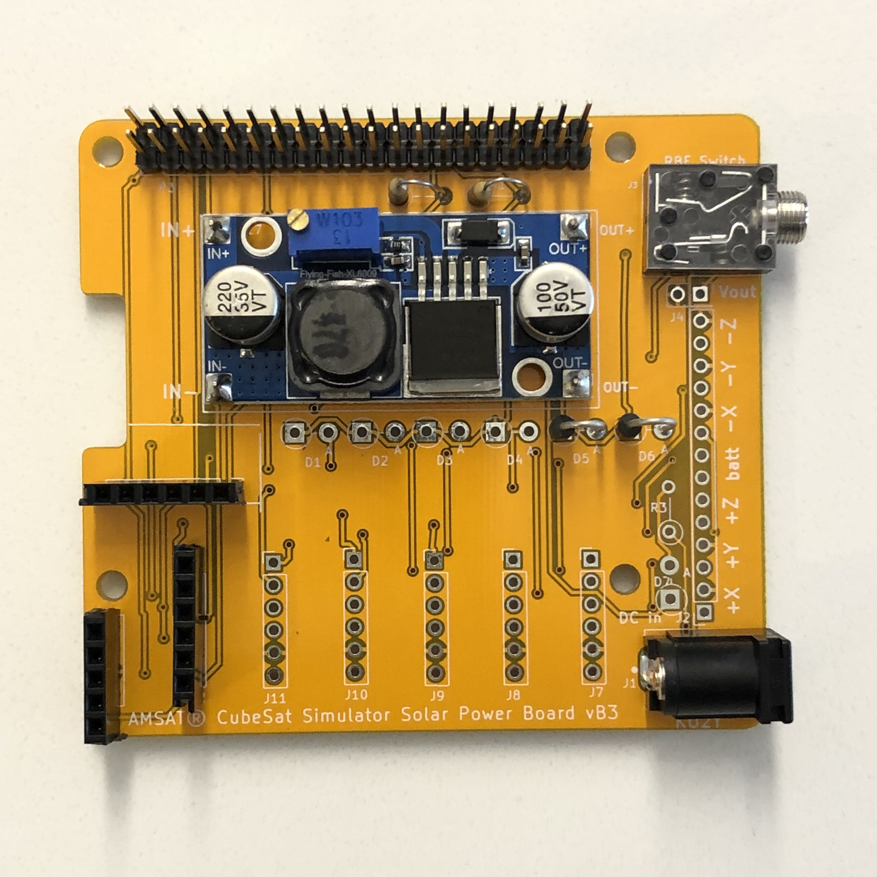
- First make the 40 pin extra long male breakaway header into a 2x20 pin header for the GPIO connector. You will need an extra stackable header, pliers, and glue, such as super glue gel. Start by inserting the 40 pin header into the stackable header, and break it in half with the pliers
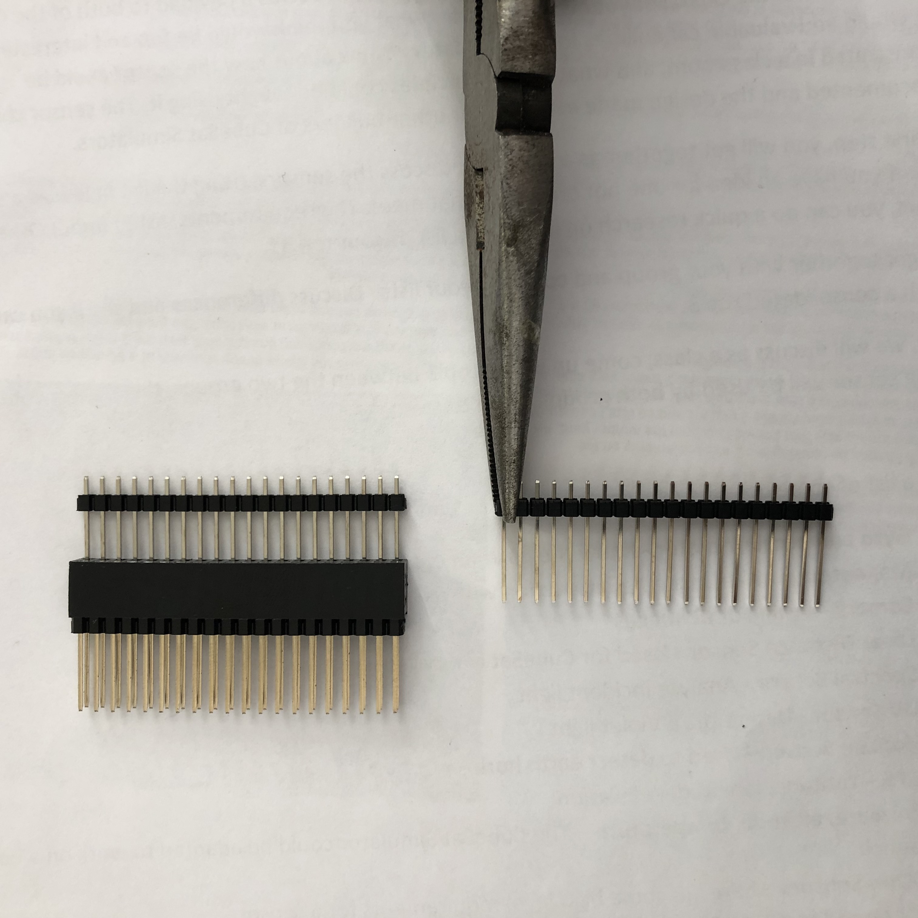
Put a very small amount of glue on several of the plastic tabs, then insert the other piece and tape to hold while the glue sets.
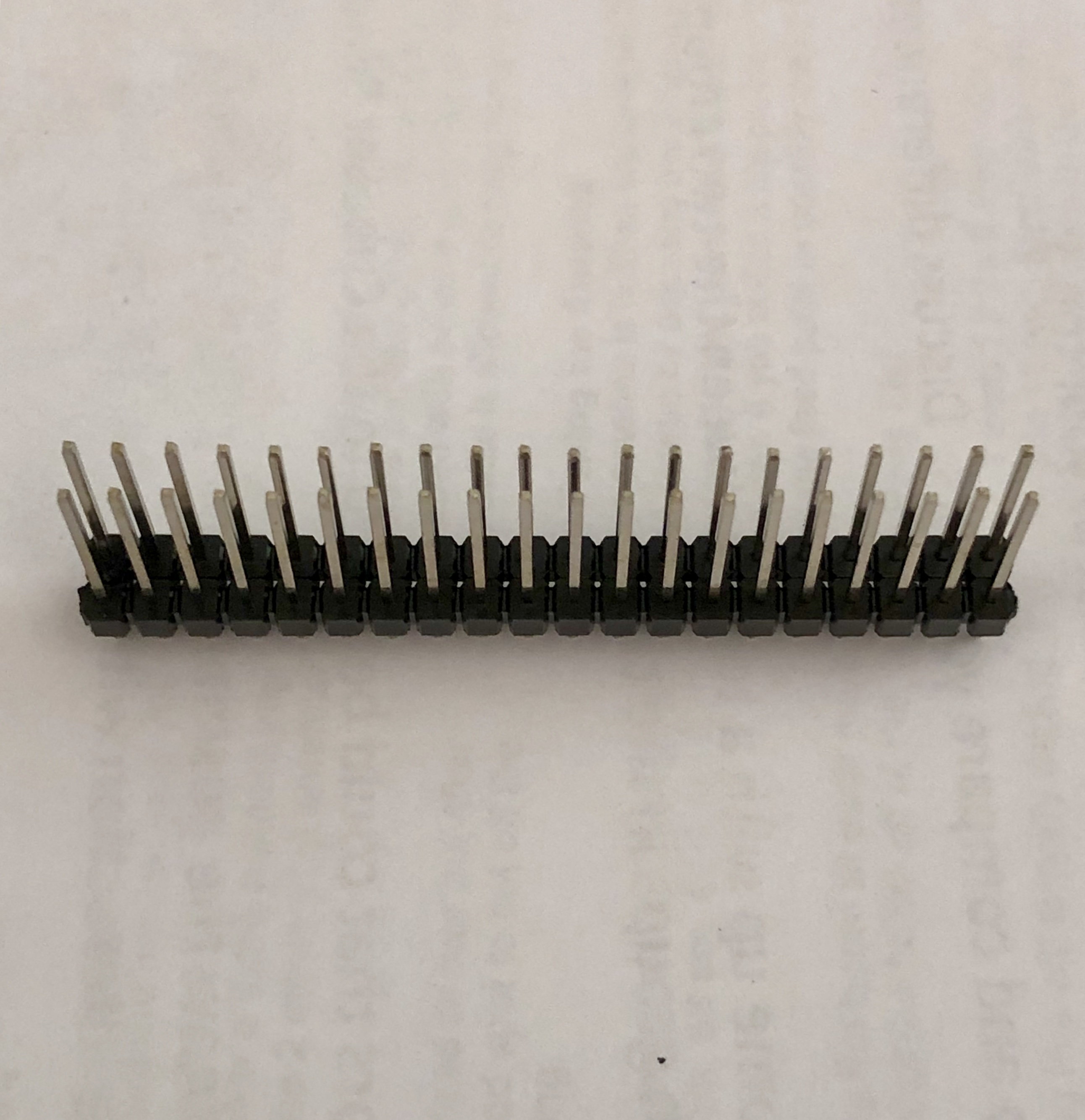
You now have an extra long 2x20 header ready to solder into the PCB:
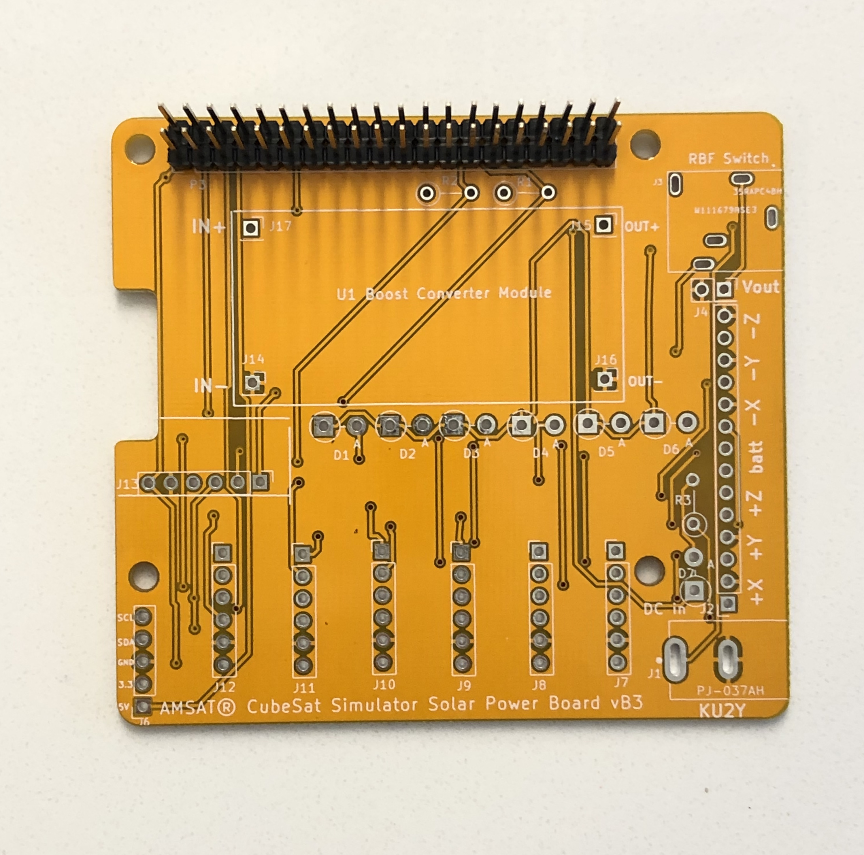
Solder the 2x20 header into place, being careful that it is at a right angle to the board. After it cools, test plugging Pi Zero W board with stackable header into the PCB.
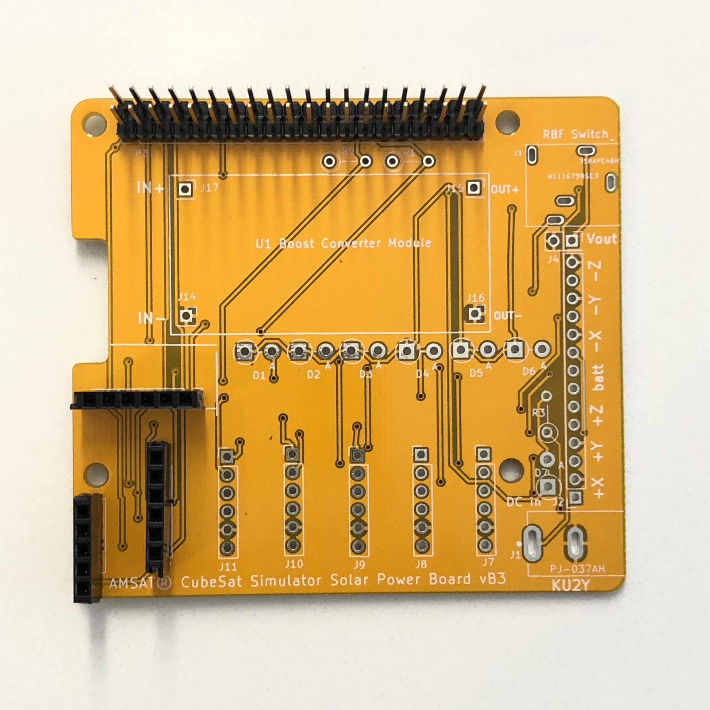
- Solder the 7x 1x6 female headers (J7, J8, J9, J10, J11, J12, J13) and 1x 1x5 female header (J6) (You could also cut two 40 pin female headers into 1x5 pin , 6x 6 pin . See https://www.instructables.com/id/How-to-cut-pin-headers/ for good tips on how to sacrifice one pin to ensure the cut header has full strength.) Note that J13 is for the -Z panel which isn't needed. This image only shows a few of the headers installed on the vB3 board:
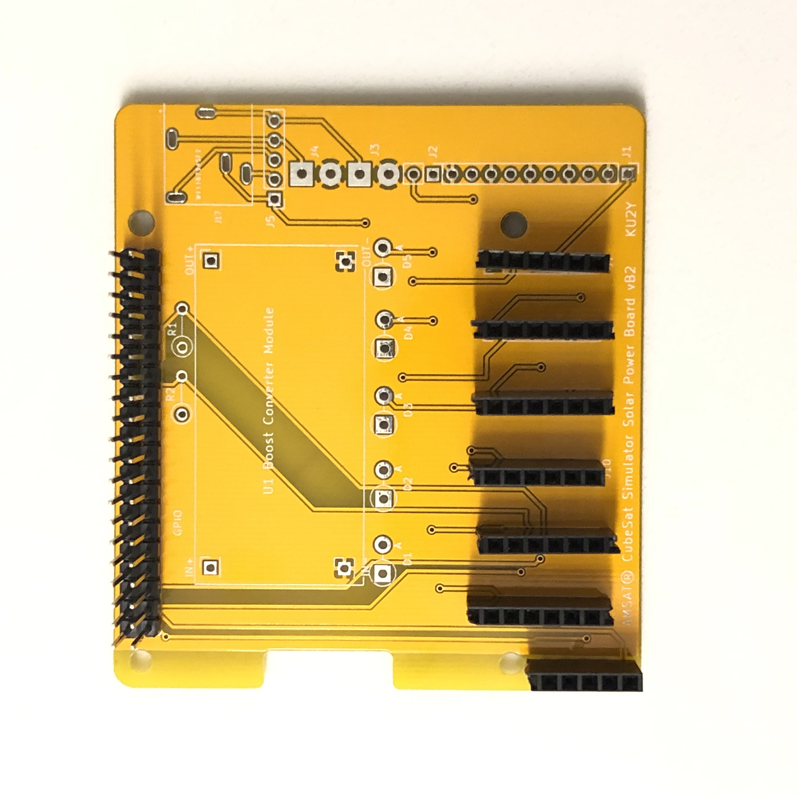
This image shows a full set installed on the vB2 board:
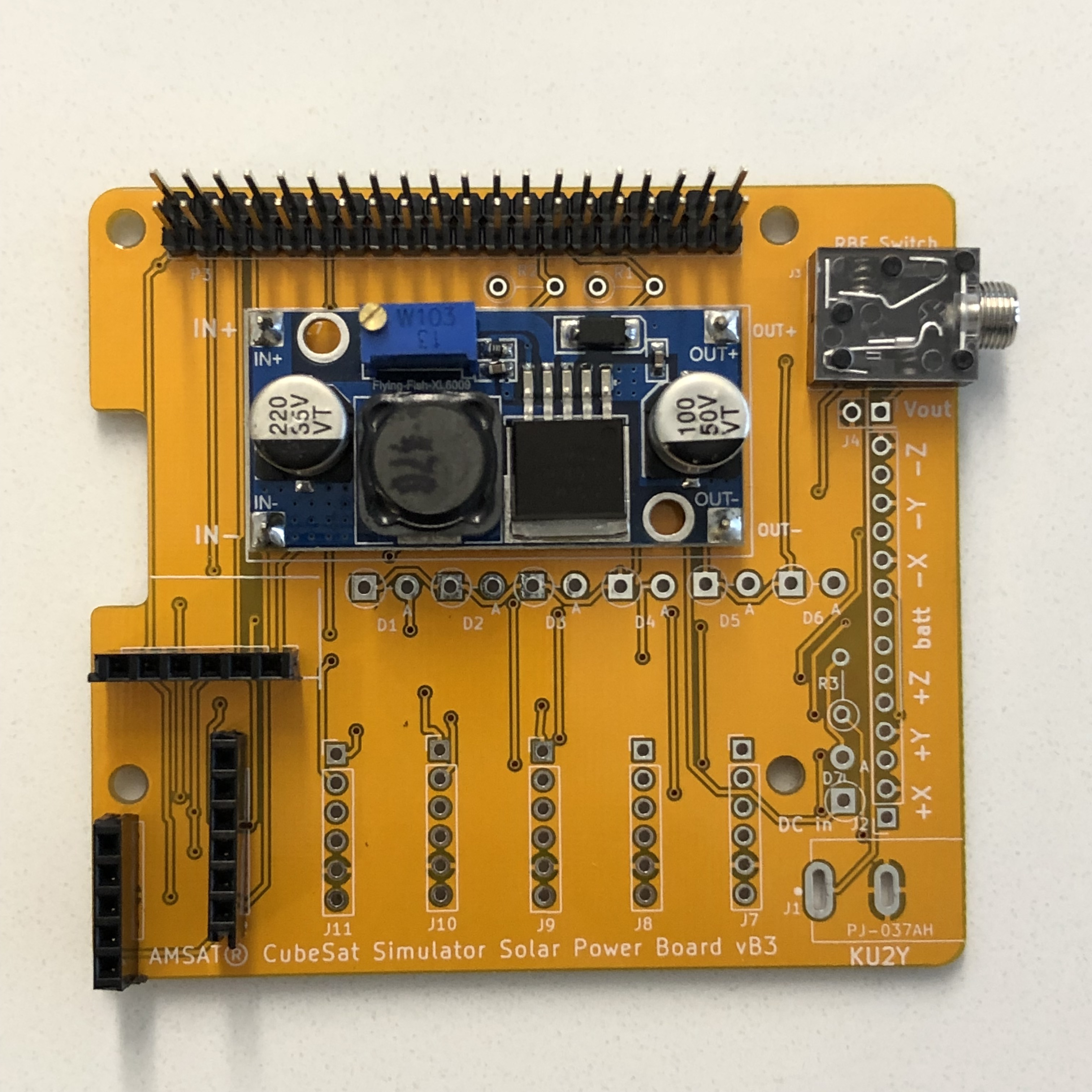
- Break off 4 single pins from the regular length male breakaway header and solder into the four terminals of the PCB U1 for the Boost Converter Module for IN+, IN-, OUT+, and OUT-. The long side of the pin should face up.
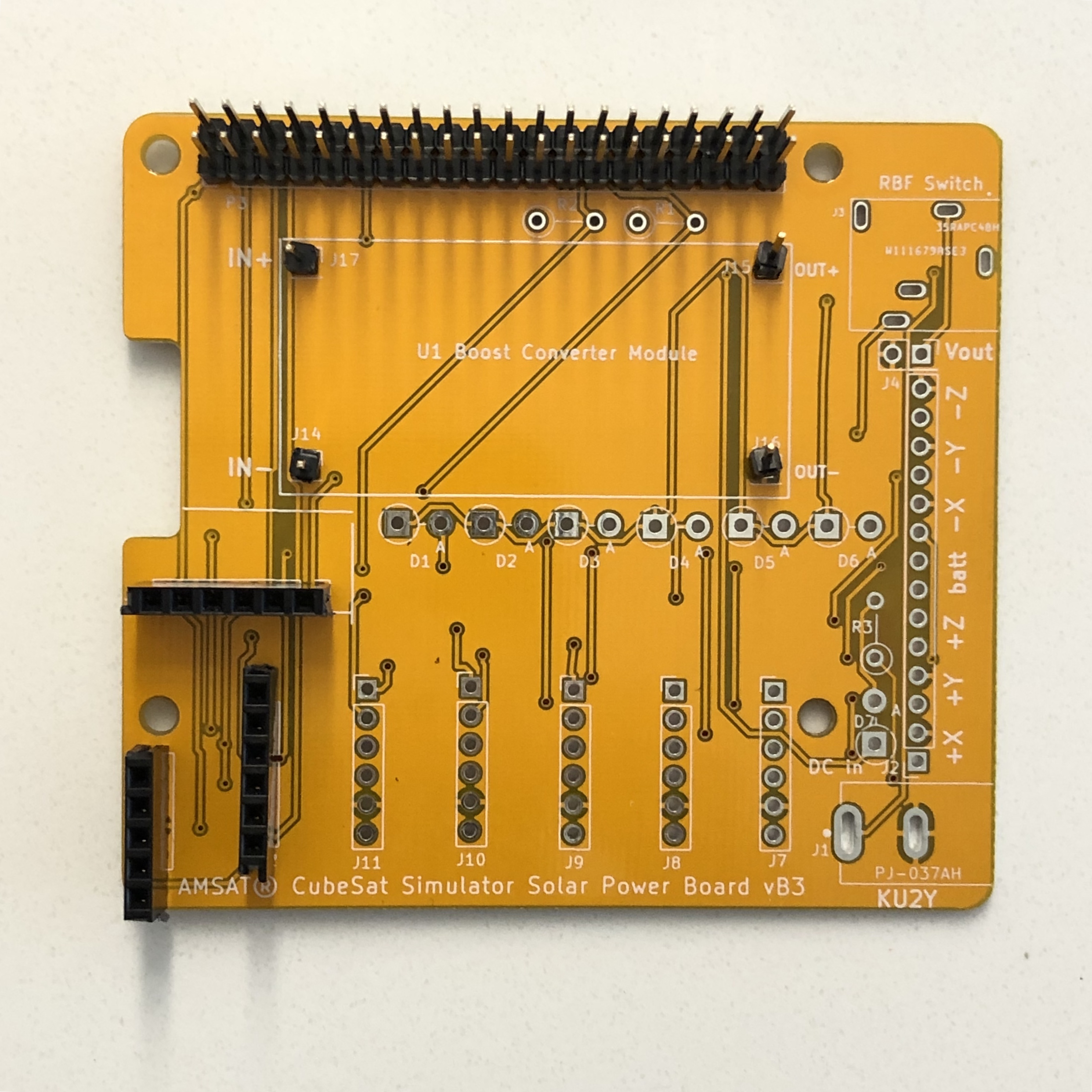
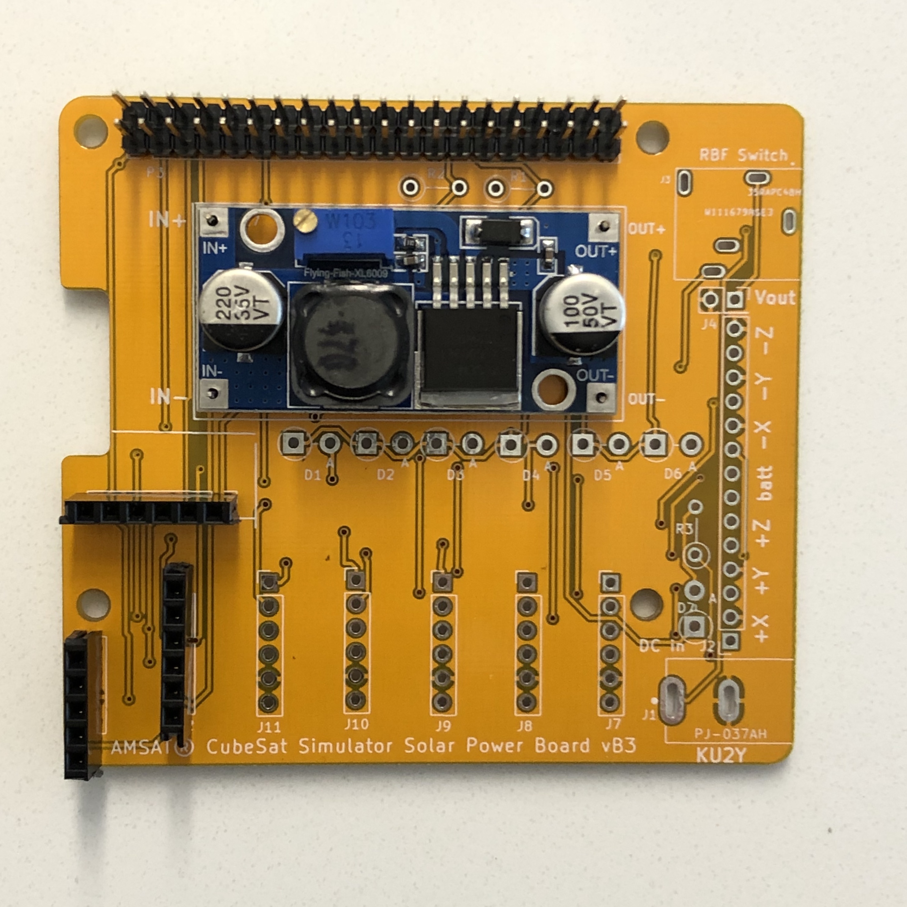
- Mount Boost Converter Module U1 onto the pins and solder the pins on the top of the board in place.
- Solder J3 RBF switch into board.
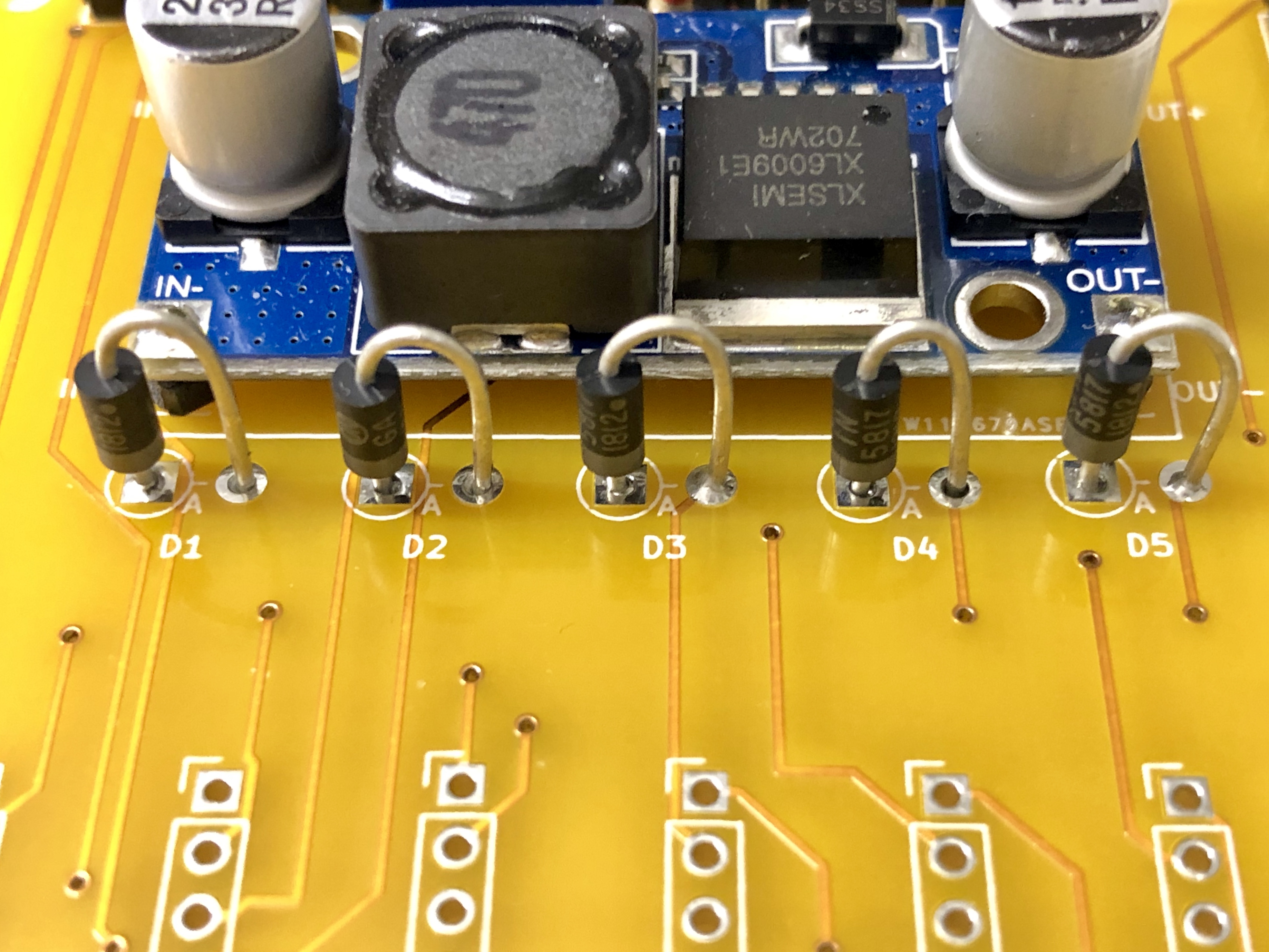
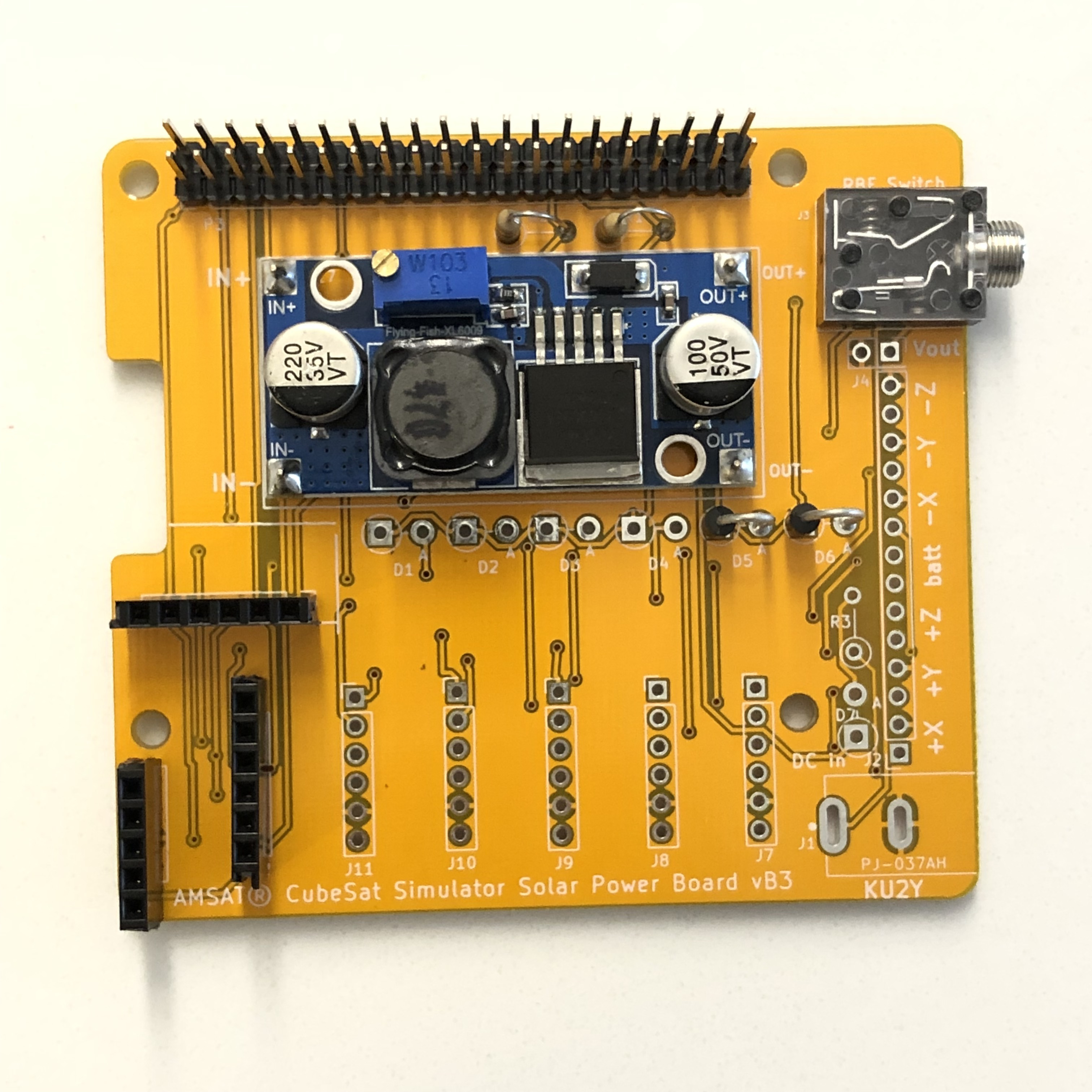
- Solder diodes D1, D2, D3, D4, and D5 vertically (Note that D6 is for the -Z panel and is not needed). Note: some solar panels have a built in diode, in which case the diode can be replaced with a jumper wire. This picture only shows D5 and D6 installed.
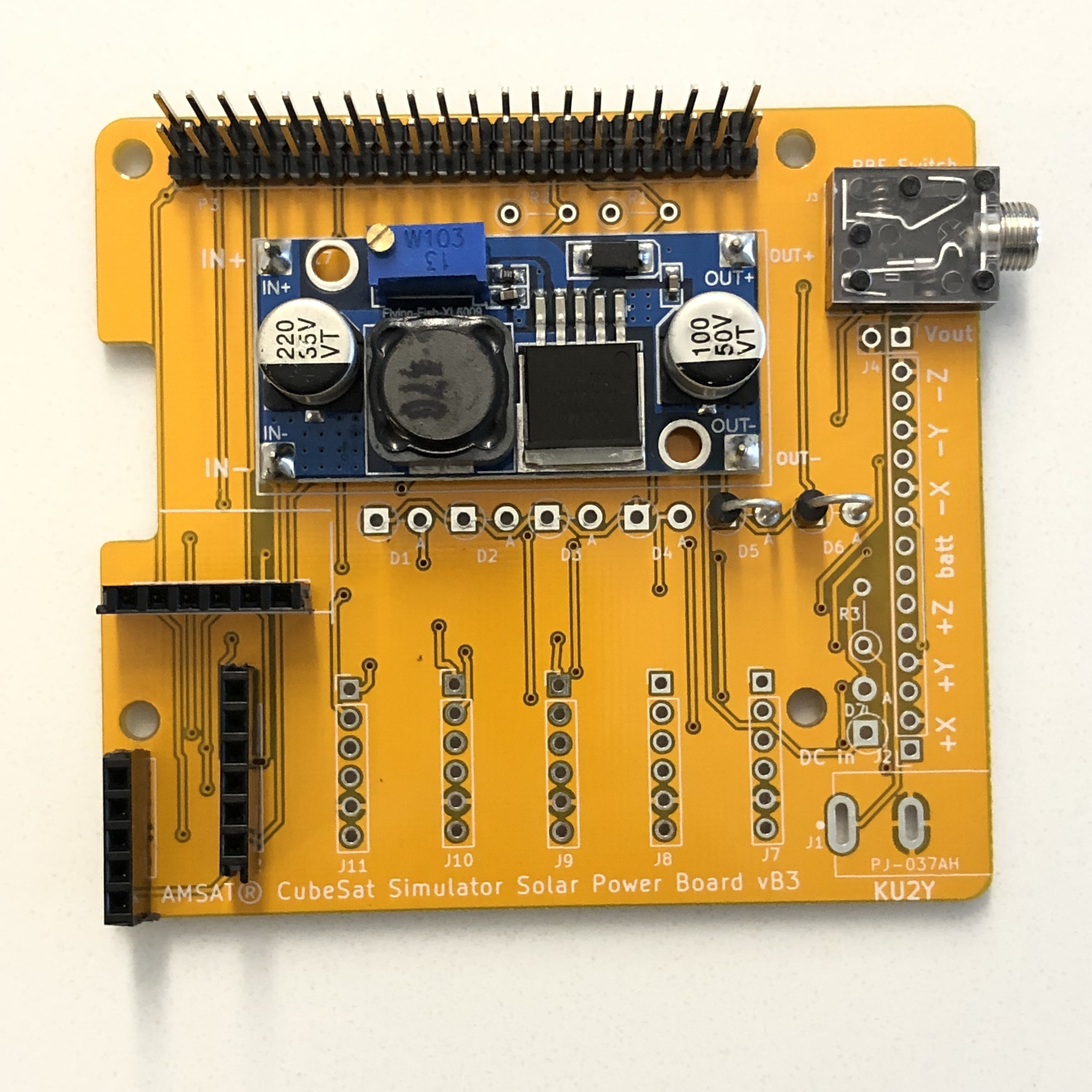
The Cathode (marked by a band on diode package) goes into the square hole (on left), while the Anode goes into the round hole (on right).
- Solder resistors R1 and R2 vertically.
- Solder the barrel connector J1 into the board.
- Cut 90 degree breakaway headers into 6x 6 pin lengths.
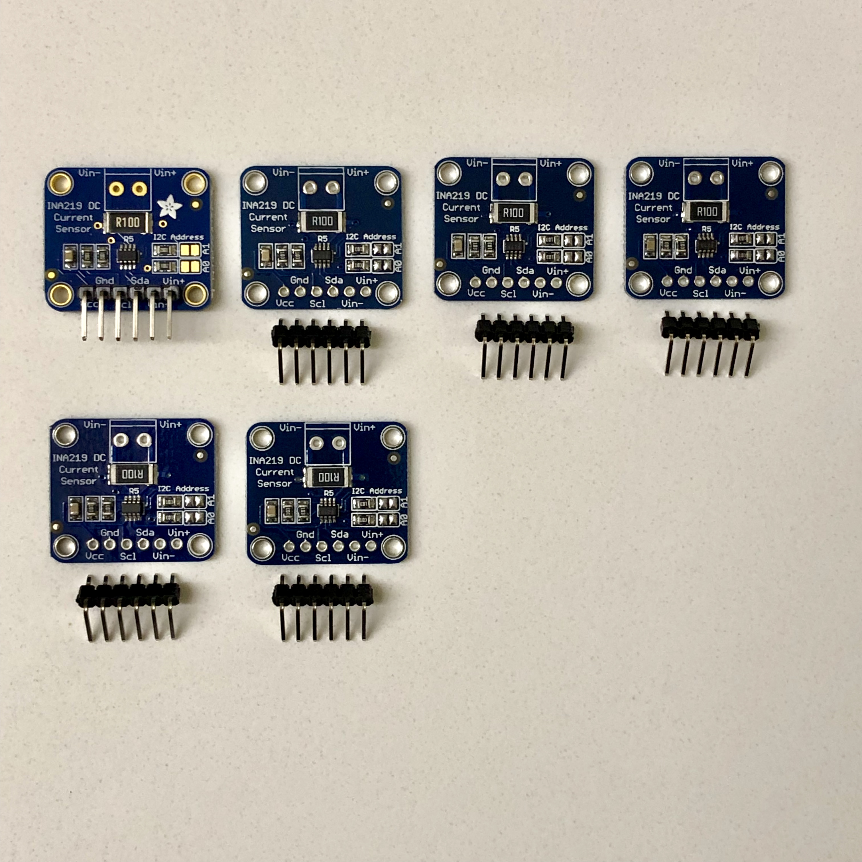
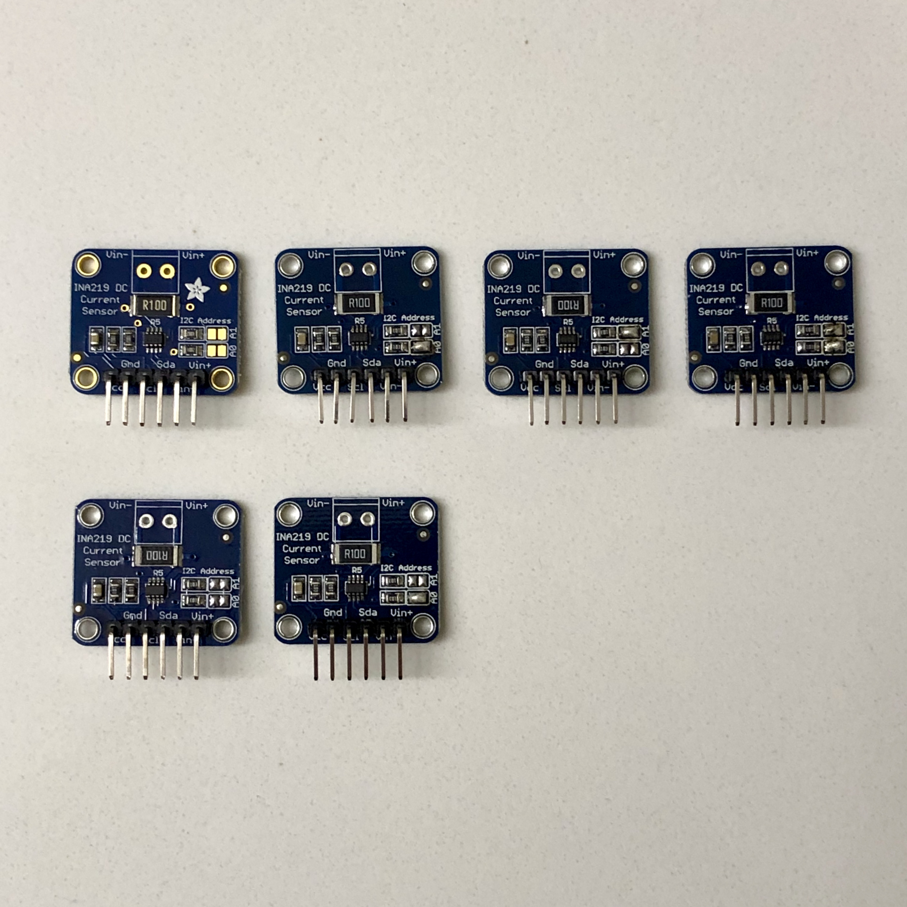
- Set the correct I2C bus address on the 6x INA219 boards by adding solder to jumpers to bridge A0 and A1 as needed. See instructions at https://learn.adafruit.com/adafruit-ina219-current-sensor-breakout/assembly (Note: do not use the pins and connectors that came with the INA219 board). Set the jumpers using this list:
- J7 +X Board: Bus /dev/i2c-1 Address = 0x40 Offset = binary 00000 (no jumpers required)
- J8 +Y Board: Bus /dev/i2c-1 Address = 0x41 Offset = binary 00001 (bridge A0)
- J9 +Z Board: Bus /dev/i2c-1 Address = 0x44 Offset = binary 00100 (bridge A1)
- J10 Vbatt Board: Bus /dev/i2c-1 Address = 0x45 Offset = binary 00101 (bridge A0 and A1)
- J11 -X Board: Bus /dev/i2c-0 Address = 0x40 Offset = binary 00000 (no jumpers required)
- J12 -Y Board: Bus /dev/i2c-0 Address = 0x41 Offset = binary 00001 (bridge A0)
- Solder the 6 pin 90 degree headers into the boards so the pins face downward.
- Solder JST RCY wires with male connector into J2 and J4 on the board. The JST RCY should be wired red and then black as shown in this image:
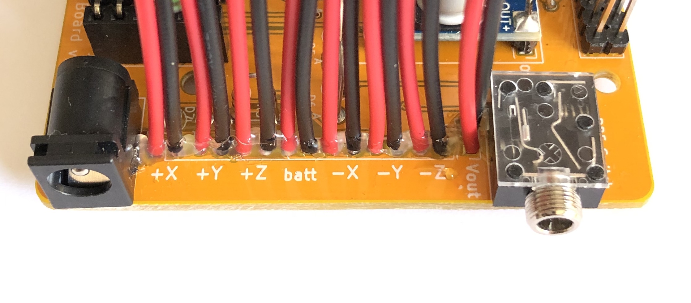
Label the connectors with a fine point sharpie. Run a bead of hot glue between the connectors and the PCB as strain relief.
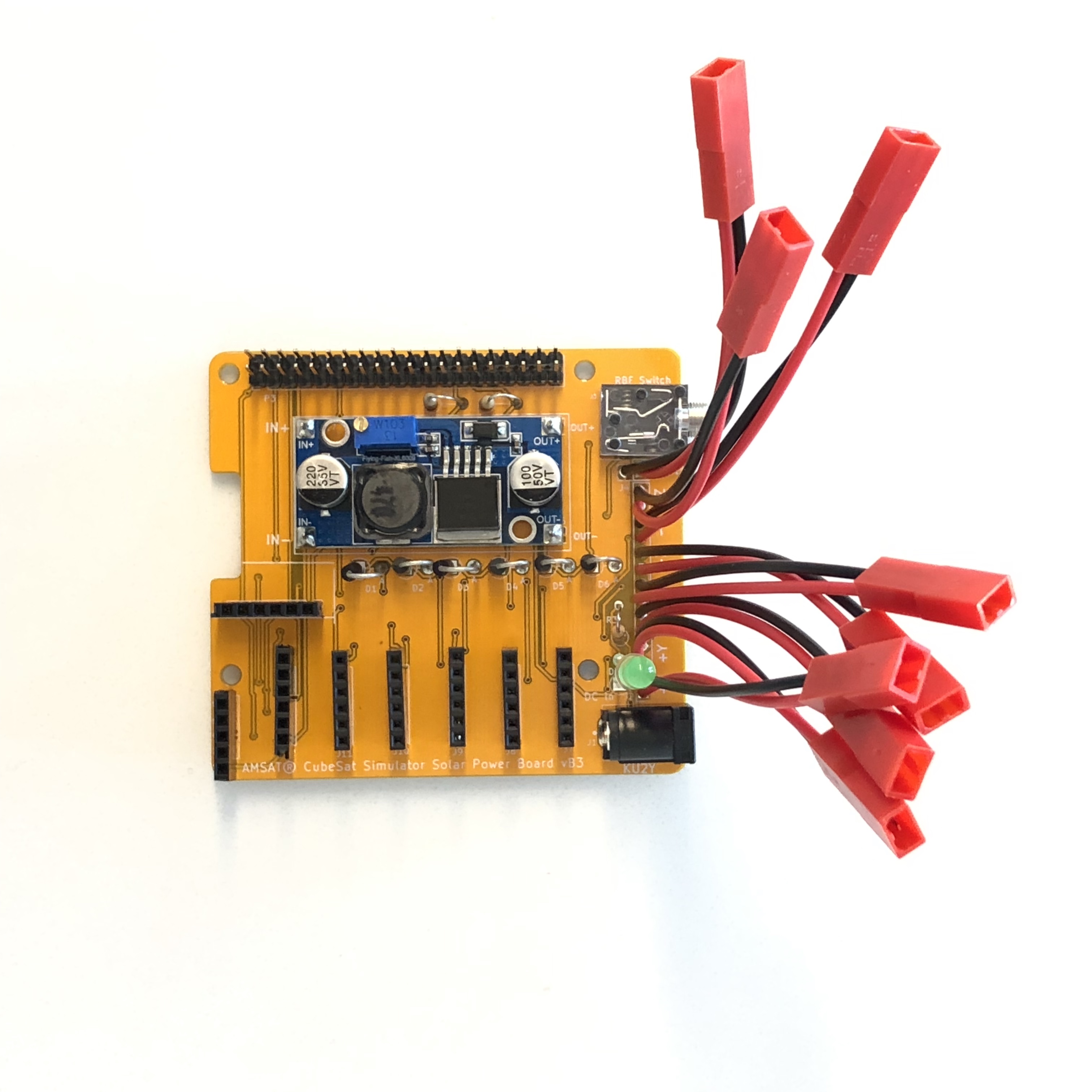
Note: D7 (green LED) and R3 are shown soldered in behind the connectors. This shows the LED soldered directly onto the board. For better illumination, you can use a 1.5 inch length of red and black wire to extend the leads so the LED is close to the top of the frame. On the LED, the Anode is labeled on the PCB with a "A" and is the longer of the leads. The other is the Cathode, which is the shorter lead, and the lead with the flat side of the lens.
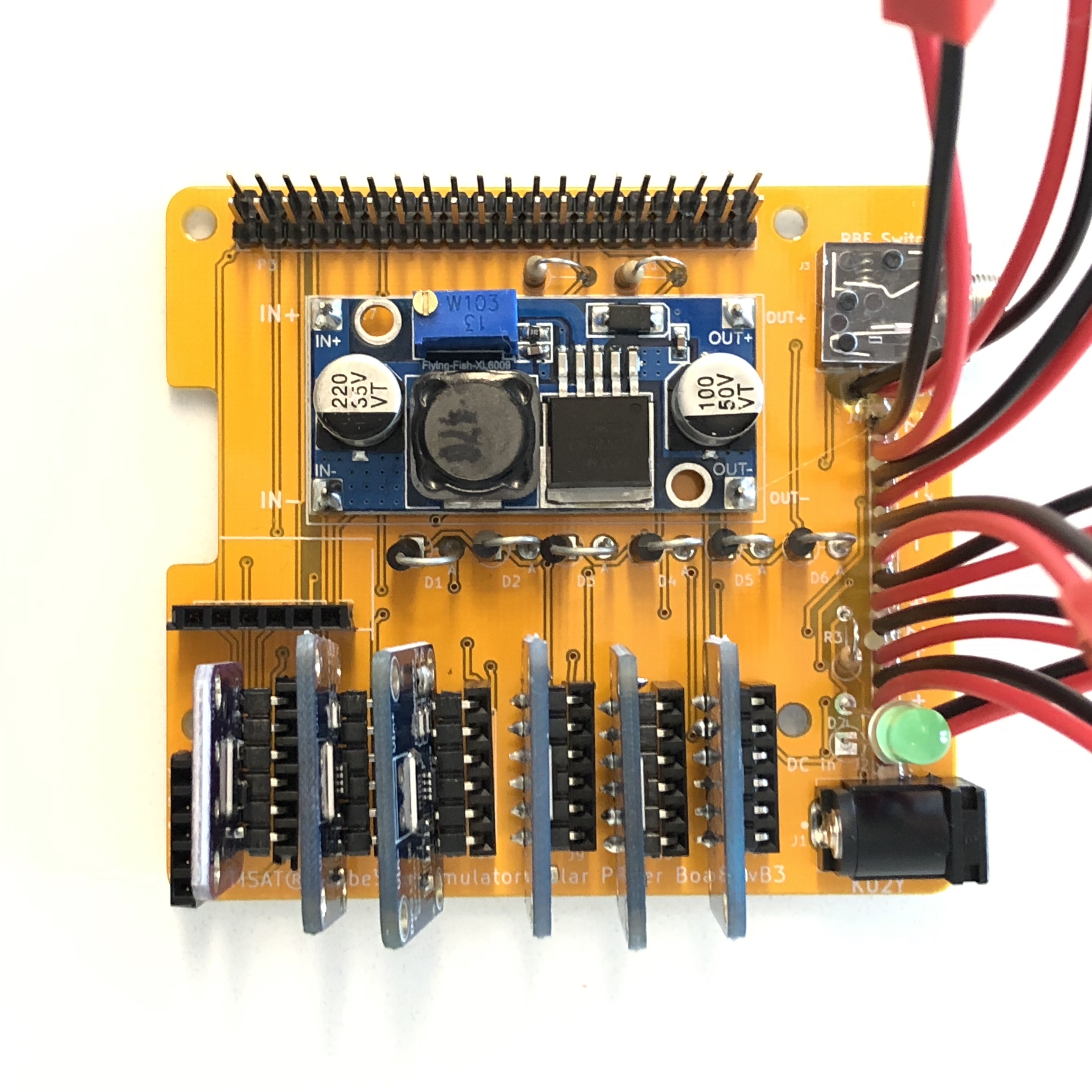
- Test fit the INA219 boards vertically into connectors J7 through J12, but do not leave them plugged in.
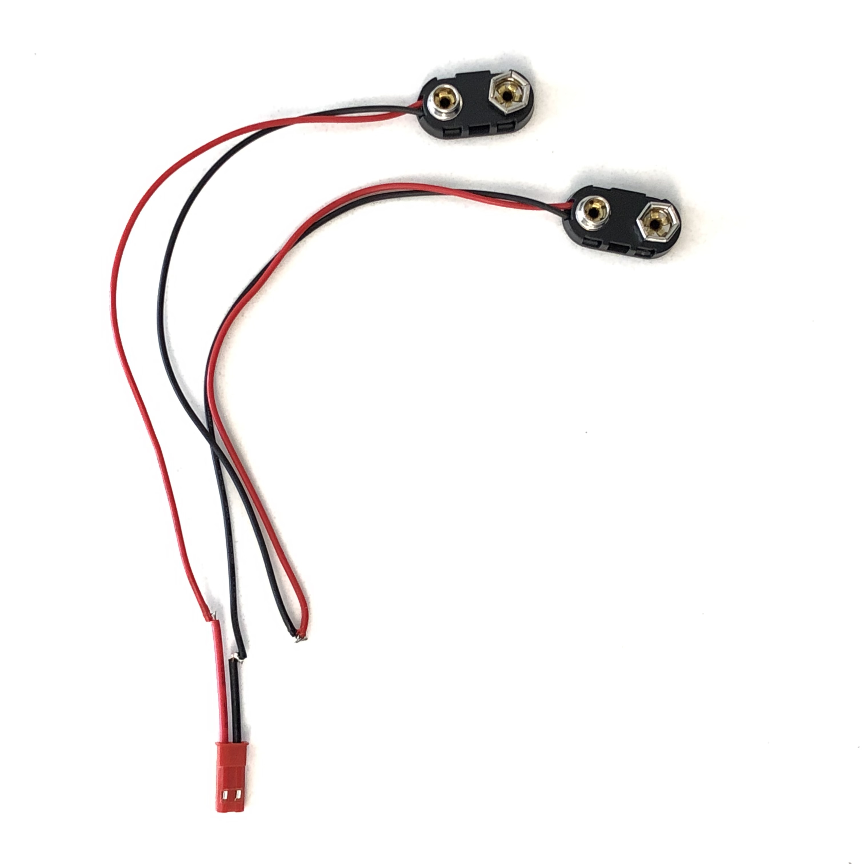
- Make the battery cable using a female JST RCY cable and 2x 9V battery connectors. Solder the black lead from one 9V connector to the red lead of the other 9V connector. Then solder the remaining red and black leads to the red and black leads of the female JST RCY connector. Heat shrink or tape the connections:
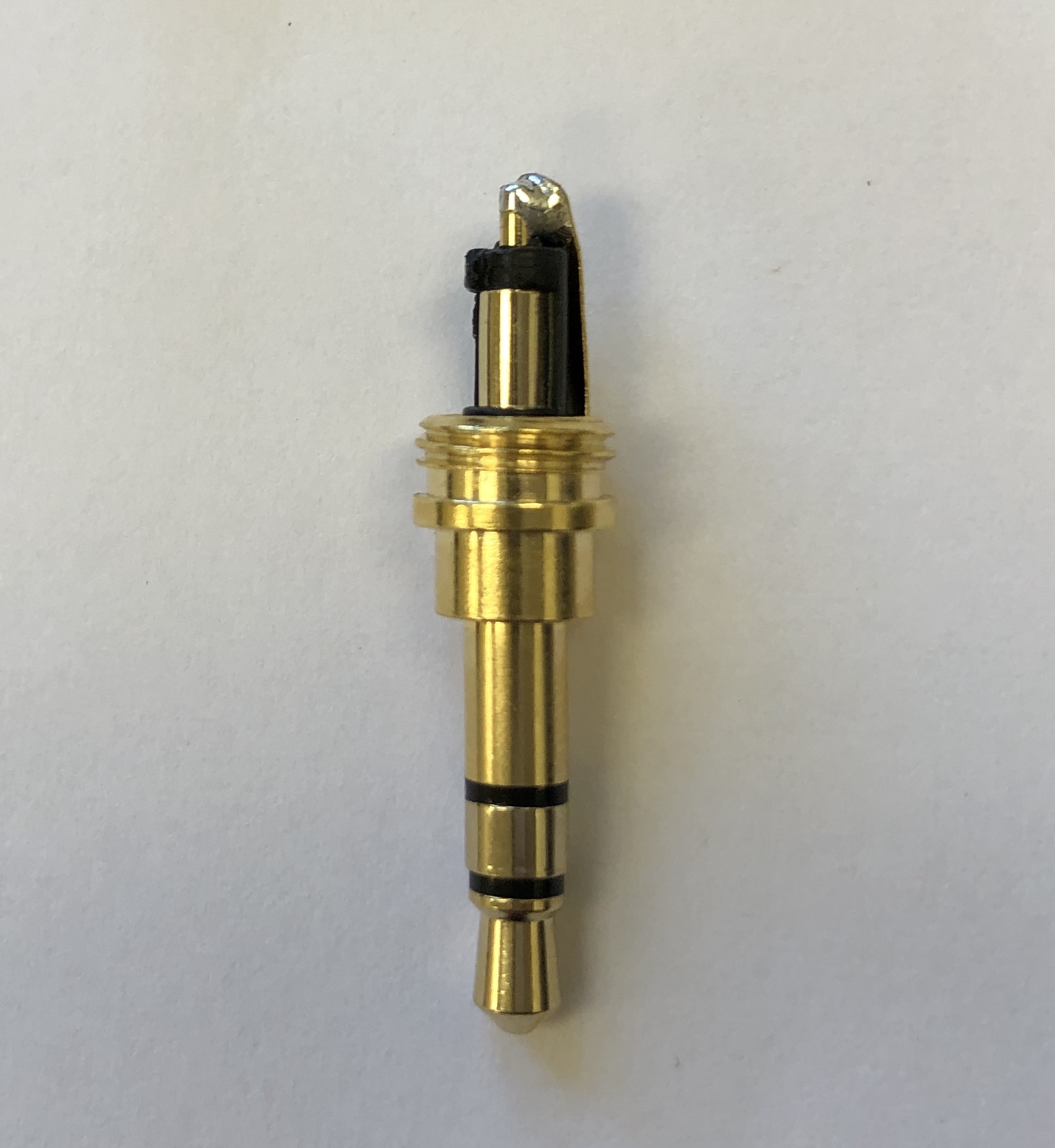
- To make the Remove Before Flight (RBF) pin, unscrew the cap on the 3.5mm stereo plug.
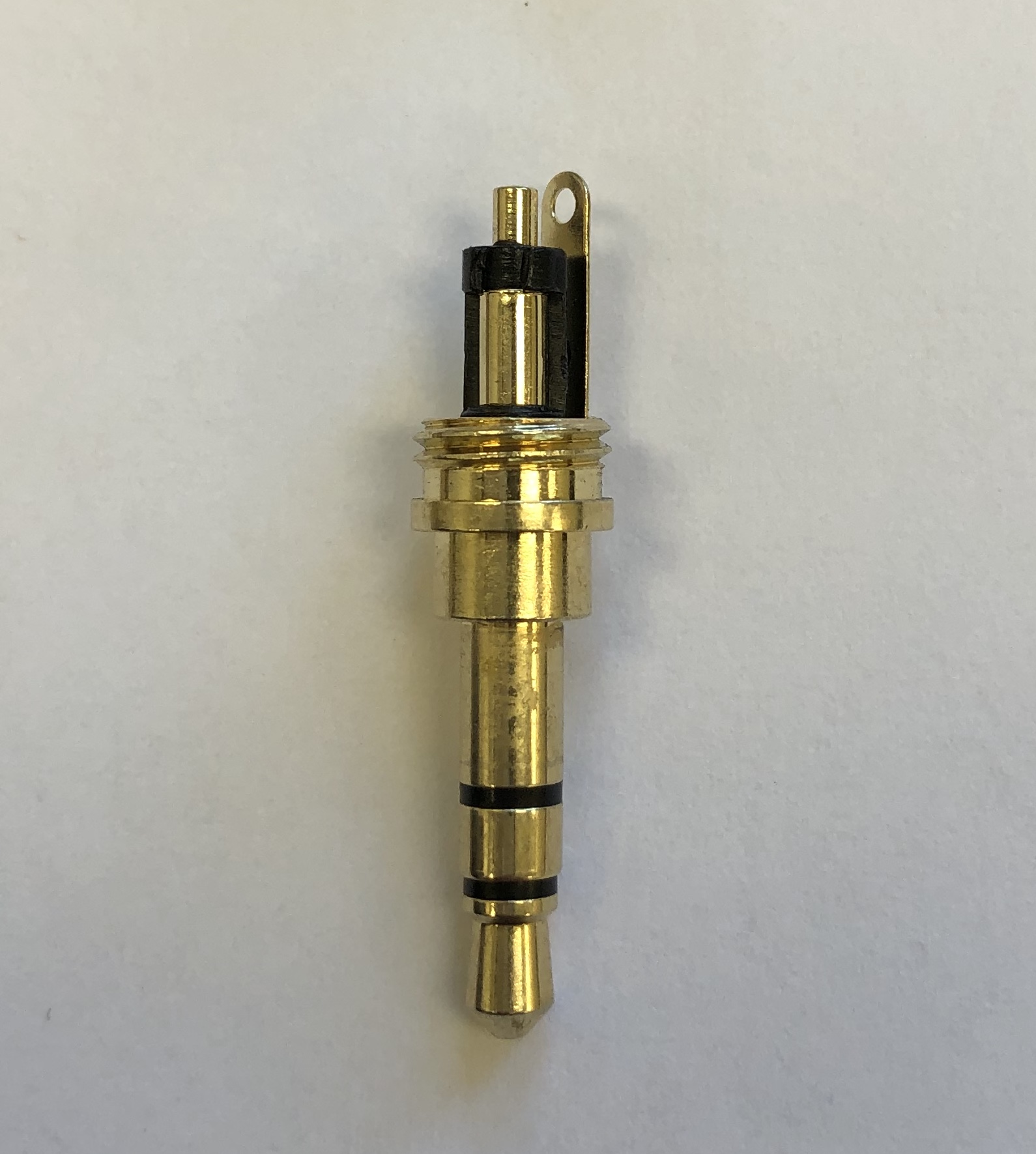
Bend the outer conductor lead against the inner conductor lead and solder:
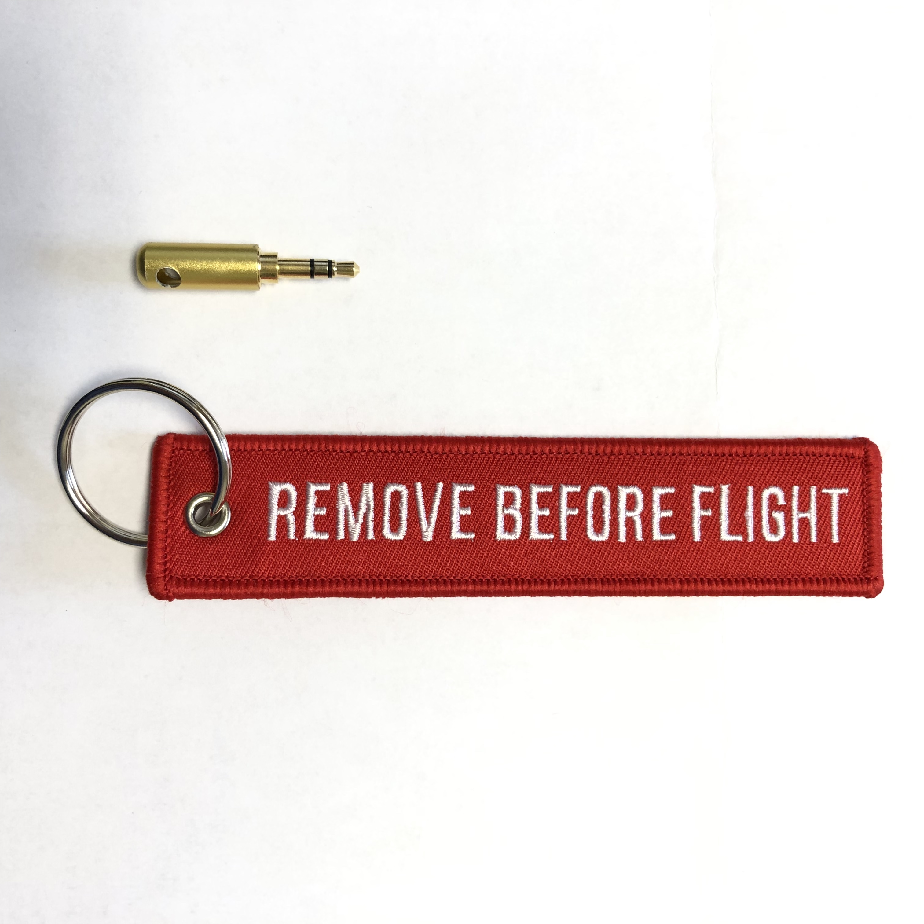
Screw the cap back on. Drill a hole through the end of the cap, then put the split ring of the RBF tag through the hole:
- The board assembly is now complete. Go on to the Solar Board Testing Instructions.