Photomask Fabrication - NanoLabStaff/nanolab GitHub Wiki
by Amund Stensrud Normann ([email protected])
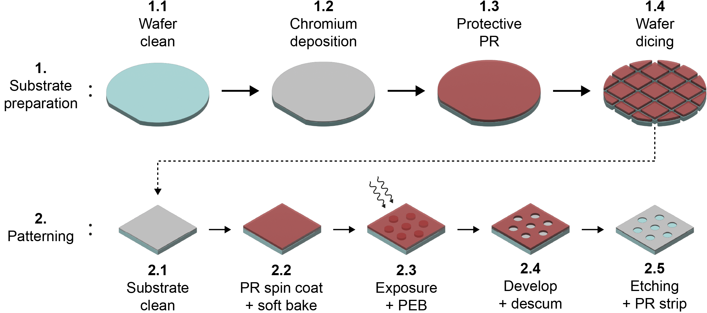
The following protocols can be used to fabricate physical photomasks for UV-lithography with features down to 2 µm. End product examples can be seen in the End Product section at the end. To fabricate photomasks the following steps will be carried out in order:
- Glass wafer preparation
- Metallization with 100 nm chromium
- Saw wafer to desired mask dimensions
- Deposition and patterning of photoresist (SPR 700)
- Etching of pattern with chromium etchant
- Strip away resist layer
These procedures were developed for a 4’’ glass wafer, but any glass surface transparent to UV light can in theory be used if it is sufficiently flat. Too rough of a surface will negatively affect the metallization and etching process.
- Clean the substrate by submerging it in acetone (ca. 1 min) followed by isopropanol (IPA, ca. 1 min), before drying with compressed nitrogen.
- Remove organic residues from the substrate with the plasma oven for 2 min at 100% power and 100% oxygen flow.
Plasma oven used: Femto Plasma Cleaner from Diener Electronics.
- Dehydration bake; heat the substrate on a hotplate for at least 3 minutes at a temperature of 150°C. Let it cool down on a cooling block.
- Secure the glass substrate to the e-beam sample holder. A 4’’ wafer can be conveniently attached to the 4’’ wafer sample holder using single-sided Kapton tape. For smaller or differently shaped samples double sided Kapton tape can be used to mount them to a 4’’ carrier wafer.
- Follow the user protocols for the e-beam evaporatorto deposit 100 nm of chromium at a rate of 5 Å/s. Remember to:
- Turn on sample rotation for better coating uniformity
- Allow vacuum to reach at least 6e-6 mbar before starting the deposition process
- Look out for anomalies in deposition rate or spitting from the chromium target during deposition
Pfeiffer E-Beam Evaporator was used
The positive photoresist SPR 700 will be spun on to the metallized wafer to protect the chromium layer from the wafer saw.
- Clean the appropriately sized spin-coater vacuum chuck
- Blow clean the substrate with compressed nitrogen before placing it on the vacuum chuck
- Spin coating of SPR 700:
- To avoid unexpected resist artifacts, turn off air flow in the spin-coater fume hood by pressing and holding the ventilation button
Spin coating with the air flow on in the fume hood has previously resulted in an uneven layer of resist with visible ring-/star like features (forum link).
- Turn on the spinner vacuum and make sure it is better than 0.7 bar
- Dispense SPR 700 with a single use pipette onto the middle of the substrate until about half of the substrate is covered
- Start the following spin process to realize an approximately 1 µm thick layer of resist: Speed = 3000 RPM, time = 30 s, acceleration = 1000 RPM/s
- Clean the backside of the substrate with a swab of acetone
- Soft bake on hotplate at 95°C for 60 seconds. Use a carrier wafer to avoid contaminating the hotplate
- Confirm resist thickness of about 1 µm by using the reflectometer Filmetrics F20
- Follow the user protocols or request assistance from one of the NanoLab engineers to use the Wafer Saw Disco 3220, located in the supporting labs area, to cut the substrate into the desired dimensions.
Note that MF26A is the preferred developer for SPR 700, but it was out of stock when these procedures were developed. Using ma-D 332/s instead of MF26A will affect the dose and development parameters relative to what is recommended in the SPR 700 data sheet, and possibly the achievable resolution.
- Use the same cleaning procedure as for the glass wafer in Step 1.1
- Use the same procedure as for the protective layer of SPR 700 applied before sawing in Step 3.1
NB! Once applied, be very careful not to damage the resist layer. Any damage to the resist risk being transferred to the chromium layer upon etching. Handle the substrate carefully with plastic tweezers instead of metal ones, or use fingers to grab it from the sides.
- Follow the user protocols for the MLA 150 to expose the substrate with the desired pattern. Use the 405 nm laser and a dose of 50 mJ/cm-2.
- Directly after exposure, do a PEB on a hotplate at 115°C for 60 seconds
- Let the substrate cool down on a cooling block.
- Develop the exposed substrate by submerging it in the developer ma-D 332/s and stirring gently every 10 seconds for a total of 50 seconds.
- Directly after developing, rinse the substrate with DI water from a squirt bottle for at least 30 seconds and/or submerge it in a bath of DI water for 1 minute
- Dry with compressed nitrogen
- Inspect the developed features, looking for signs of damage or over-/under exposure or development.
A plasma descum is needed prior to etching to remove residual resist remaining in developed areas.
- Descum the substrate by using the plasma oven for 1 min at 50% power and 50% oxygen flow.
- Patterned substrate to be etched
- Plastic tweezers
- Glass beaker (yellow circle), large enough to fit substrate - for chromium etchant
- Glass beaker (yellow circle), large enough to fit substrate - for rinsing with water
- Chromium etchant standard (Sigma Aldrich, product nr: 651826) - NB! A buddy is needed for handling this chemical in NanoLab
- Wipes
- Timer
Note that chromium etchant etches most other metals as well, so metal tweezers or sample carriers should not be used.
For the features etched here (5-100 µm) the etch rate was found to be about 20 Å/s. However, this can vary a lot depending on feature dimensions and density, as well as the age of the etchant solution. To calculate the required etching time, doing an initial experiment to determine the relevant etch rate for the desired pattern is recommended.
- Put on PPE for handling corrosive chemicals (apron, face shield, yellow acid gloves)
- Fill one beaker with DI-water.
- Pour enough chromium etchant into the small glass beaker to cover the sample, then close the lid
- Holding the sample with plastic tweezers, submerge it into the chromium etchant
- Wait for 50 seconds (20 Å/s * 50 s = 1000 Å = 100 nm)
- Transfer the sample into the water bath to quench the etching process. Use the water gun to actively rinse the sample for 30-60 seconds, then let it sit in the water bath for at least 3 more minutes.
The same etchant solution can be reused multiple times and should be stored in a personal bottle for later use. Be sure to label the storage bottle appropriately.
1. Inspect the etched sample prior to removing the resist layer. Look for signs of damage, residues or insufficient etching. 2. With the sample held at an incline, use a spray bottle of acetone to wash away the resist. > Note that simply submerging the sample in acetone, without first spraying at an incline, was found to sometimes produce a brown smudge after etching, possibly due to chromium residues clinging to the resist layer being redeposited on the sample. 3. Transfer the sample into an ultrasonic bath in acetone to remove stubborn resist. The descum process can harden layers of the resist, making it a bit harder to remove. 4. Submerge the sample in IPA for about 1 minute before drying it off with compressed nitrogenAttached are some figures of masks I made throughout my thesis.
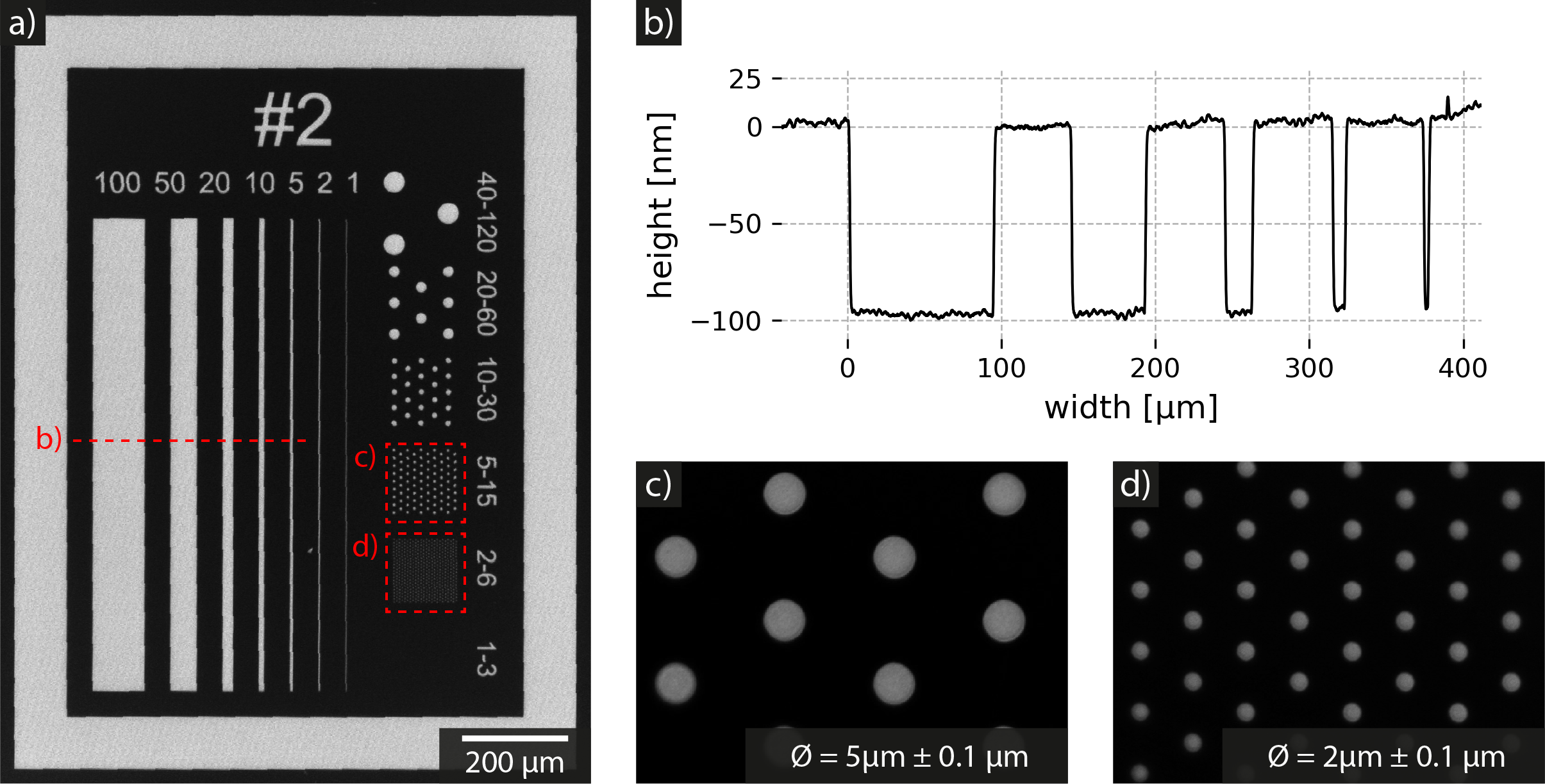 This was a test mask to get the dose, development and etching parameters right. The numbers above the lines in (a) are their respective widths in µm. The etching profile appears to be decent, as seen in (b). The numbers to the right of the hexagonally dotted areas in (a) are the circles' diameter and spacing in the format diameter-spacing
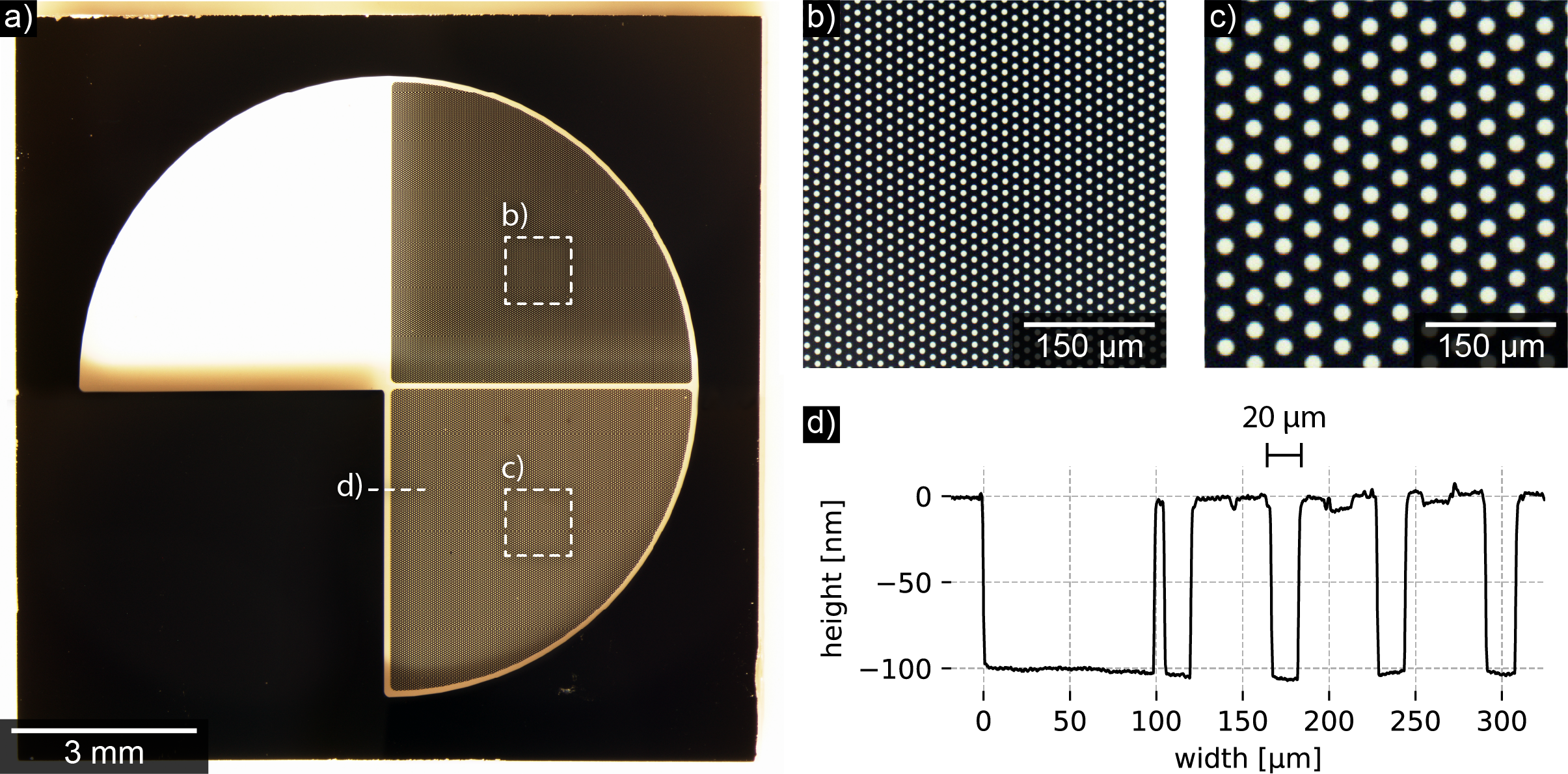 This was a mask I used for inclined photolithography (protocols for that can be found here), with large arrays of hexagonally arrayed circles. The top right area of (a) shows 10 µm circles spaced by 20 µm and (b) the bottom right shows 20 µm circles spaced by 40 µm (c). I have made a script to simplify the design of masks with large hexagonal arrays in CleWin. Check it out here: CleHexArr (GitHub).