Inclined Photolithography of SU 8 (45 µm) - NanoLabStaff/nanolab GitHub Wiki
by Amund Stensrud Normann ([email protected])
Inclined photolithography is a niche variation of conventional lithography, where the exposure step is done at an incline to achieve oblique features. While traditional lithography is limited to extrusions of 2D patterns with sidewalls normal to the substrate, inclined lithography can be used to achieve tilted features:
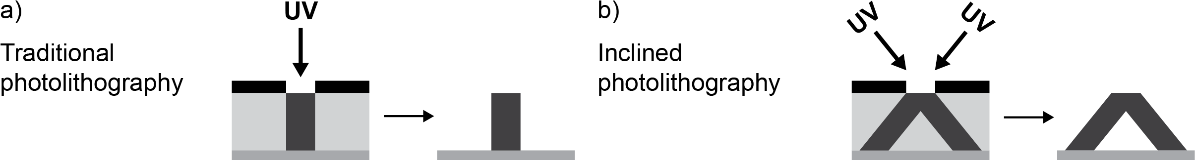 Figure 1: Illustration of how traditional planar photolithography yields extruded 2D features with sidewalls normal to the substrate (a), while inclined photolithography can be used to achieve oblique structures (b).
The following protocols detail how inclined photolithography of 45 µm thick SU-8 3050 can be carried out at NTNU NanoLab to fabricate 3D tripod structures, like the ones seen under the End Product section at the end. Other 3D structures can be realized by altering the proposed exposure setup and by using different photomasks. Have a look at this article by Han et al. (2004) for some other examples.
I have included some of my own tips and experiences from working with the thick SU-8 resist, as it took a considerable amount of trial and error to get right. Most of the following steps should be equally applicable to ordinary lithography of SU-8 as well. Note that the protocols were developed for 24 x 24 mm square glass substrates. For other dimensions or materials, small adjustments, e.g. to spin coating parameters or exposure dose, might be necessary.
The figure below illustrates the main steps of the inclined lithography process:
- Substrate cleaning
- Substrate priming (HMDS)
- Spin coating of SU-8
- Soft bake
- Inclined exposure with rotation in between exposures x3
- Post exposure bake (PEB)
- Development
- Hard bake
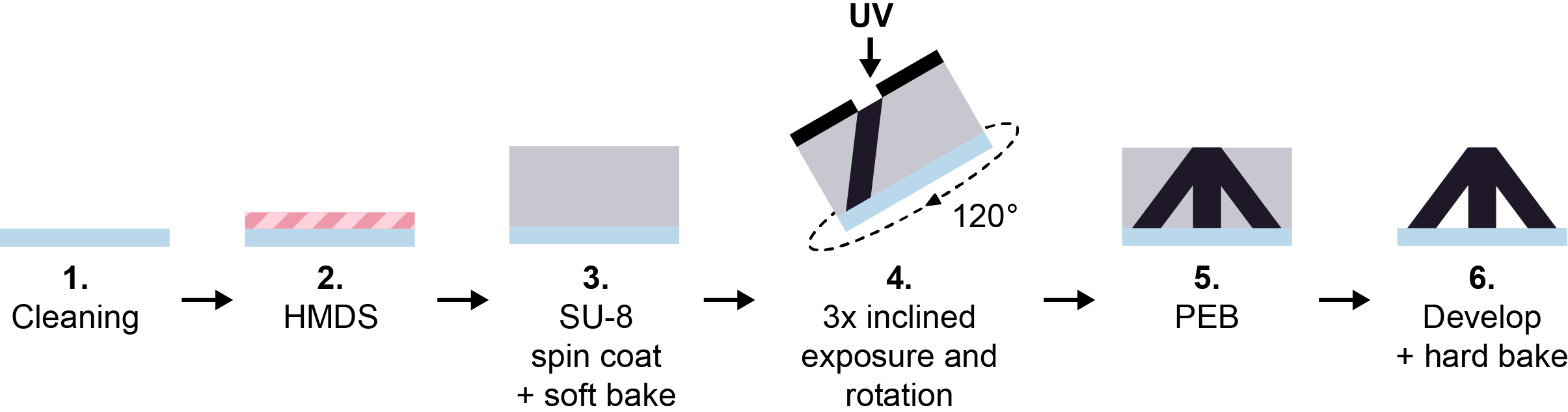 Figure 2: Illustration of the main steps involved in the inclined lithography process
- Place the samples in the HMDS vacuum desiccator
- Use a disposable syringe to put a few drops of HMDS into a small beaker
I used 1, 1, 1, 3, 3, 3-Hexamethyldisilazane from Acros Organics, product nr: 430851000
- Put the beaker in the desiccator, together with the samples
- Turn on the vacuum pump and let the desiccator pump for about 10 min
- Isolate the desiccator and turn off the vacuum pump
- Leave the desiccator for the desired amount of time
- Retrieve the samples
Optional step: If adhesion is a problem, an additional dehydration bake (5-10 min on 150°C hotplate) can be added after HMDS and immediately prior to the spin coating to make sure there is no moisture on the substrate. HMDS is known to be very sensitive to moisture and believed to degrade rapidly in humid environments. This step appeared to improve adhesion in my case, but I was also trying other parameters at the same time, so I am unsure whether this added baking step was a decisive factor.
-
Clean the appropriately sized spin-coater vacuum chuck
-
Blow clean (and cool if heated) the substrate with compressed nitrogen before placing it on the vacuum chuck
-
Turn on the spinner vacuum and make sure it is better than 0.7 bar
-
Carefully pour SU-8 3050 from a small bottle onto the substrate center until it forms a puddle covering about 1/3 - 2/3 of the sample surface
From experience, a tiny bit too much is usually better than too little. Excess SU-8 will be spun off without notably affecting the resulting thickness or profile, but too little resist will invariably yield spin artifacts.
-
Start the following spin process to realize a 45 µm thick layer of resist
- Speed = 300 RPM, time = 10 s, acceleration = 300 RPM/s
- Speed = 3000 RPM, time = 30 s, acceleration = 300 RPM/s
- Speed = 4000 RPM, time = 5 s, acceleration = 1000 RPM/s
This final, high accelleration spin step is included to spin off some of the edge bead, without affecting the resist thickness too much.
-
Use a swab of acetone to remove any resist on the backside of the substrate, or be sure to use a clean carrier wafer for subsequent soft baking.
Soft baking of SU-8 will reduce the solvent level and solidify the applied film. If adhesion is a problem, a relaxation period of up to one hour can be introduced after spin coating and prior to soft baking. This should help reduce some tensions in the resist, and/or at the substrate interface. Soft baking temperature, as for any heat treatment of SU-8, should preferably be ramped **slowly** up and down to reduce interfacial tensions between SU-8 and the resist. **Never use a cooling block to cool down SU-8 samples!** The rapid change in temperature is very likely to cause delamination.Further tips: The high viscosity of SU-8 can make it a bit tricky to handle, and this step might require some practice to get right. If possible, pour from a half-full bottle instead of a full one, as this makes it easier to handle. As a tip to stop pouring, tilt the bottle back while simultaneously twisting it. While doing this, try to avoid spilling any resist outside of the centered puddle; this will usually negatively affect the spin coating uniformity. Getting the timing right will require some experience, as the high viscocity of SU-8 keeps it flowing for a while after the bottle has been tilted back. Note that it will grow thicker over time due to age and being repeatedly exposed to air. Make sure to firmly close the lid immediately after each use!
If available, use a programmable hot-plate in the following manner:
A manual hotplate can be used as well, but including some sort of temperature ramping is usually beneficial for more stable results
- Place the substrates on a clean carrier-wafer to avoid contaminating the hot-plates
- Start the soft baking program at 30°C for 5 min
- Ramp the temperature up to 95°C over 30 min (2°C/min)
- Bake at 95°C for 35 min
About 15 min at 95°C is what is recommended in the data sheet, but for me this did not bring the solvent level down enough to avoid the photomask sticking to the resist after exposure. If you are using the MLA for exposure, however, 15 min might be sufficient.
- Set the temperature to 30°C and let the sample cool down slowly with the hot plate for about one hour before retrieving it
Being a big slab of metal, the hotplates cool down very slowly even when set to the lowest available temperature.
The inclined exposure setup assembled for these protocols (displayed in Figure 3 below) consists of three main components: (1) a UV-curing lamp, (2) a 3D printed stage for tilt and rotation of the samples, and (3) a physical photomask:
-
UV-source: The UV-curing lamp, purchased from Extral Light Store (China) via aliexpress.com (link to product), consists of a 2x4 array of uncollimated UV-LED (365 nm) diodes. The UV-Optometer from Krüss was used to determine the source's exposure effect at 21 mW/cm2 for 365 nm radiation 5 cm away from the source. A stand-alone UV-source is needed for inclined lithography as the available exposure systems at NanoLab, i.e. the MLA or MA6, are designed to operate in very close proximity to the substrate, limiting any substantial tilting
-
Sample stage: The setup used here, consisting of a stage and tower component, was designed in TinkerCAD and 3D printed on the Ultimaker 2+. The design files have been made publicly available at the TinkerCAD website (link). The sample stage to use will depend on the desired exposure angle, and if any rotation is to be carried out in between exposures. Note that the refractive index of SU-8 (n=1.6) limits the achievable angle to about 39°, without some trickery .
-
Photomask and shadow mask: Physical photomasks are needed for the exposure step. See separate protocols here on how to fabricate these. To ensure sufficient contact between mask and resist, make sure the mask is small enough to fit inside the SU-8 edge bead region. Use a shadow mask of aluminum foil to cover surrounding resist from exposure (See (i) in Figure 3 below).
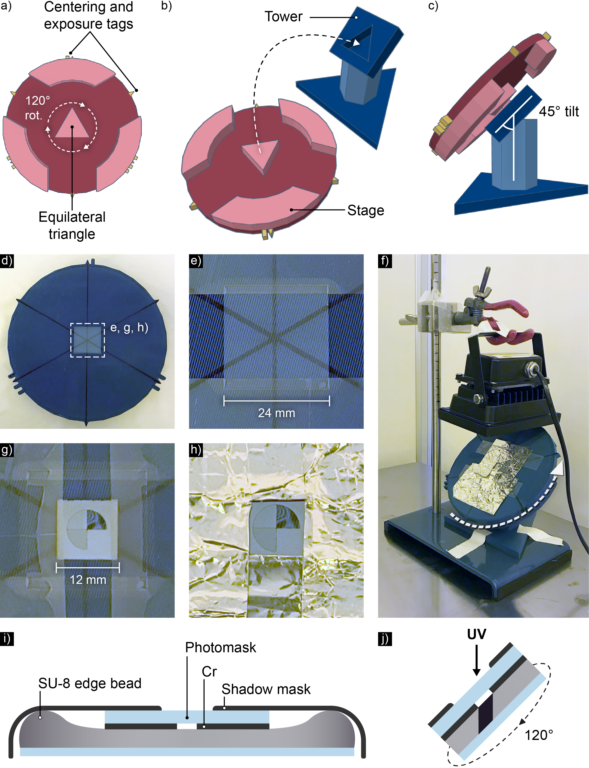
Figure 3: 3D model of the inclined exposure setup (a-c) and depiction of the sample mounting and exposure steps (d-j). 3D model (a-c): Tags along the stage perimeter can be used for substrate centering and to keep track of the number of exposures carried out (a). The equilateral triangle lock and key design between the tower and stage allows for convenient 120° rotation after each exposure (a, b). Joined together, the stage is tilted at a 45° angle relative to the normal line and UV-source (c). Exposure process (d-j): The sample (24 x 24 mm) is centered on the stage (d) and fastened using Scotch tape (e). The patterned photomask (12 x 12 mm) is pressed into contact with the resist and secured with tape (f). A shadow mask of aluminum foil is used to shield surrounding resist from exposure (g). The stage is joined with the tower at a 45° angle beneath the UV-source and can be rotated 120° between exposures (h). Sample cross sections are illustrated in i) and j). Note how the photomask is made to fit inside the edge bead region of the resist, enabling good contact in the area to be patterned, while a shadow mask is placed on top to cover the surrounding resist from exposure. Illustrations are not to scale.
To use the assembled exposure setup, manage substrates according to the following steps (illustrated in Figure 3 above):
- Position the sample on the stage center and use Scotch tape to secure it
- Press the photomask firmly into contact with the resist, inside the edge bead region and with the patterned chromium layer faced down. Secure it to the sample and stage with Scotch tape along the edges.
- Cut out a shadow mask of aluminum foil and use double-sided Kapton tape to secure it to the photomask. Make sure it does not overlap the region to be patterned.
- Join the stage to the tower at a 45° angle.
- Cover the entire setup with the opaque UV-shield dustbin before exposing
- Turn on the UV-source for 25 s (equals a dose of 525 mJ/cm2)
- Rotate the stage 120°
- Repeat step 4-7 two more times, for a total of three exposures
The tags along the stage perimeter can be used to keep track of how many exposures has been carried out.
- Gently remove the tape securing the photomask and carefully pry loose the mask from the substrate.
- Finally, carefully remove the tape securing the sample to the stage
A post exposure bake (PEB) is necessary to drive the cross-linking reacting of SU-8. It is typically done at 95°C, but can be done at as low as 55°C (see [this](https://www.spiedigitallibrary.org/journals/journal-of-micro-nanolithography-mems-and-moems/volume-4/issue-4/043008/Low-stress-ultra-thick-SU-8-UV-photolithography-process-for/10.1117/1.2117108.short) paper) to minimize heat induced swelling and subsequent delamination or deformation of the exposed features. The following PEB procedure on a programmable hotplate is advised:The photomask can be cleaned in an ultrasonic bath of acetone for 1-2 min, followed by a bath in IPA for 1 min, dried with compressed nitrogen and reused for multiple exposures.
- Place the samples on a clean carrier wafer to not contaminate the hotplates
- Start the baking program at 30°C for 5 min
- Ramp the temperature up to 60°C over 30 min (1°C/min)
- Bake at 60°C for 1 hour
- Set the temperature to 30°C and and let the samples slowly cool down with the hot plate for about one hour before retrieving them
- Using the wafer carrier, submerge the samples in mr-Dev 600 for a total of 7 min
- Stir gently every 30 s
- After 2, 4 and 6 minutes in the developer, use a disposable pipette to douse the sample with developer from the same beaker
This is done to add some extra agitation and possibly wash away stubborn resist.
- After 7 min, submerge the samples in IPA for 1 min
- Very gently, blow dry the samples with compressed nitrogen
Some structures can be very fragile at this point, so be careful when drying. Once dried and hard baked, however, they are usually a lot more stable.
- Place the samples on a clean carrier wafer to not contaminate the hotplates
- Start the baking program at 30°C for 2 min
- Ramp the temperature up to 180°C over 20 min (7.5°C/min)
- Bake at 180°C for 60 min
I used 60 min mainly for biocompatibility reasons, but everything between 15-120 min should suffice.
- Set the temperature to 30°C and and let the samples slowly cool down with the hot plate for about one hour before retrieving them
Attached are some figures of 3D structures I made throughout my thesis, using the process described above.
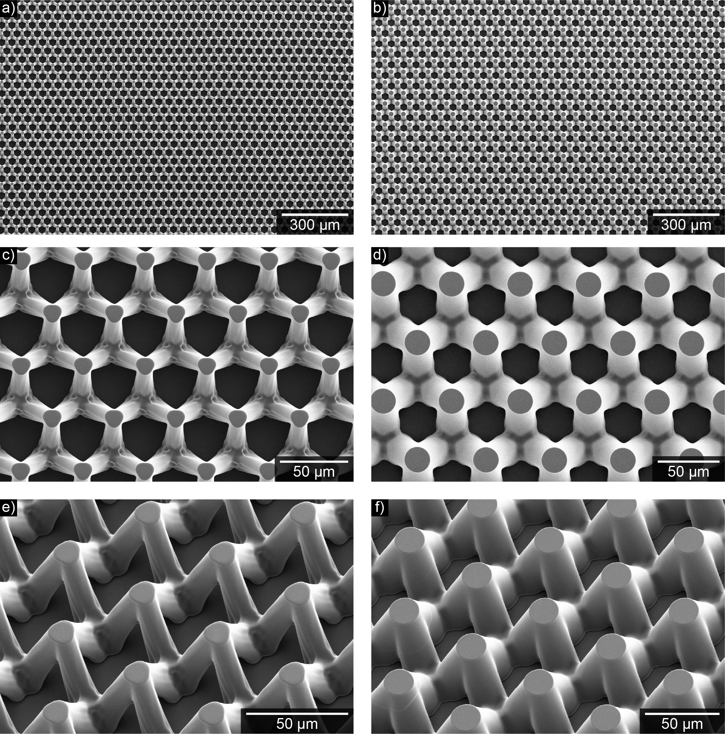 Figure 4: Electron micrographs of 45 µm tall interlinked tripods of SU-8 on glass, as realized by inclined lithography. Tripods with leg diameter of 10 µm and 20 µm are depicted in the left and right column, respectively. The spacing is 45 µm for 10 µm tripods and 55 µm for 20 µm tripods. Portrayed by a)-d), the inclined lithography technique established can reliably be used to fabricate large areas of homogeneous tripods linked at the bottom of each leg. A 45° tilted view of the interlinked tripods can be seen in e) and f).
Developing a stable process for inclined lithography took a considerable amount of optimization. However, along the way, I acquired a number of artistic electron micrographs whenever the fabrication did not go according to plan:
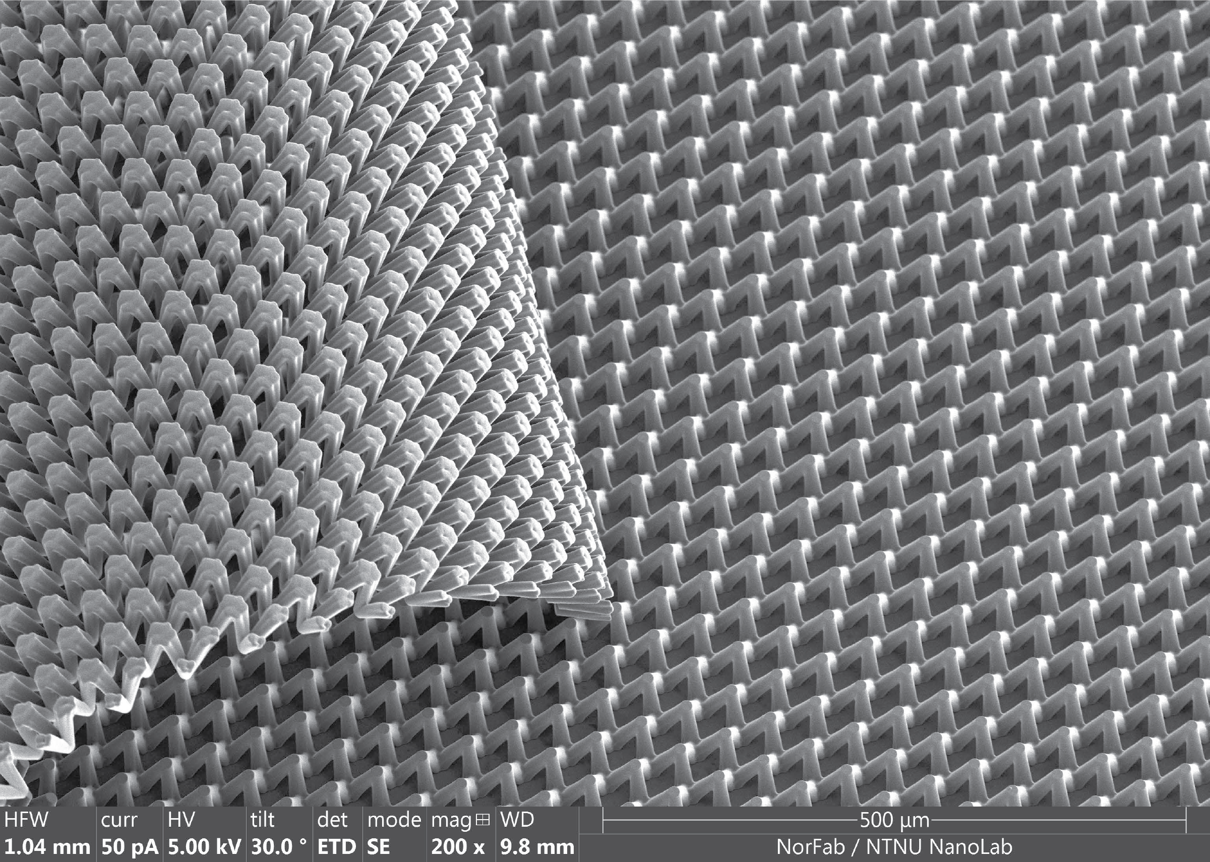 Figure 5: Delamination has caused the interlinked structures to peel away from the substrate and fold back on themselves, resulting in this artistic image
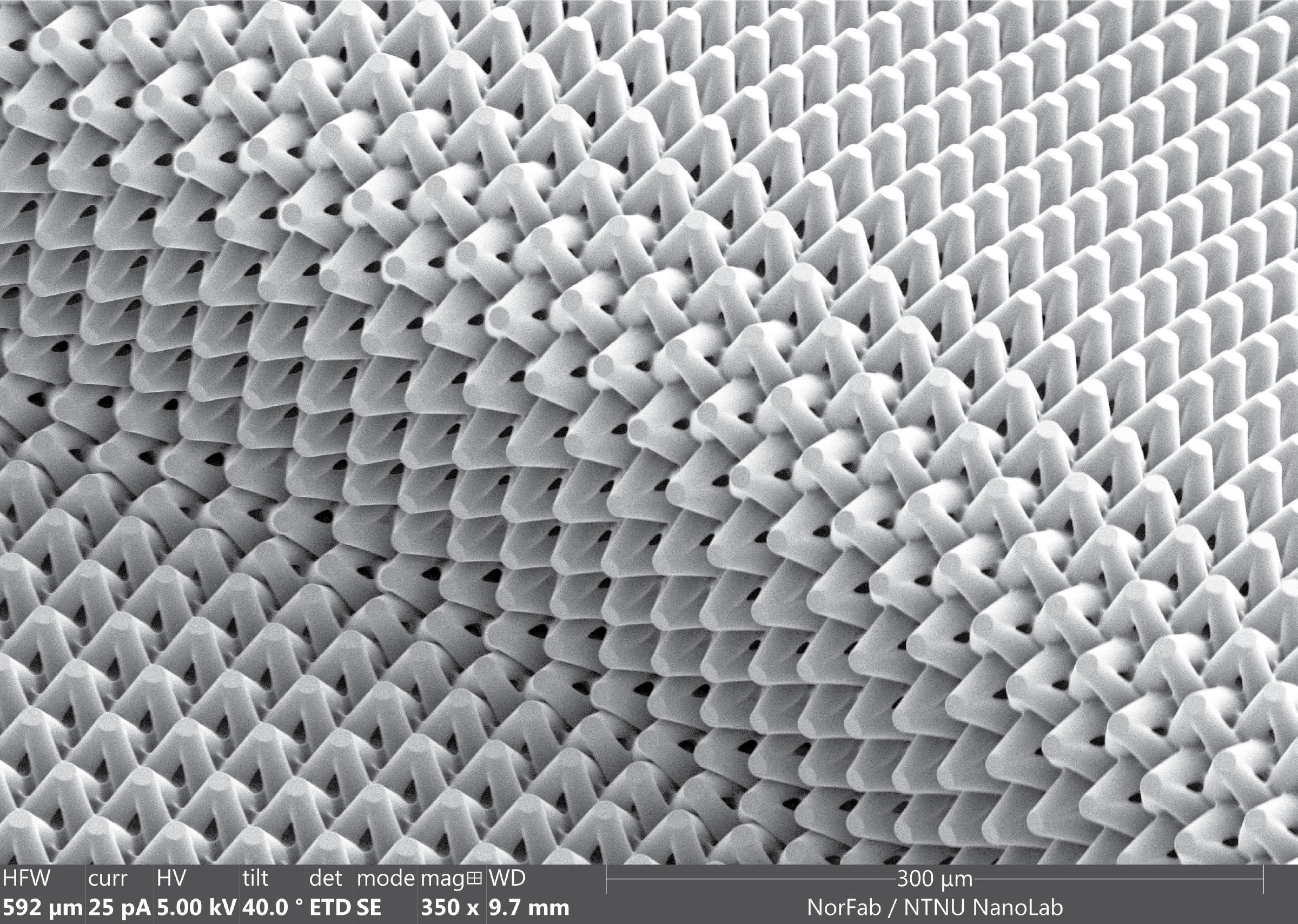 Figure 6: Here, swelling during the post exposure bake has caused the overlapping structures to wrinkle and fold. Interestingly, with this image an optical illusion can sometimes be seen, where the part of the image not immediately in focus seems to shift and wave slightly. This image won the NanoLab Image Contest 2022, for which I am very grateful.
Interestingly, when exposed on Si-wafers instead of glass, UV-reflection made for some interesting V-shapes. Furthermore, for the larger features, reflection happened in the chromium mask as well, resulting in N-shaped features with only one exposure step:
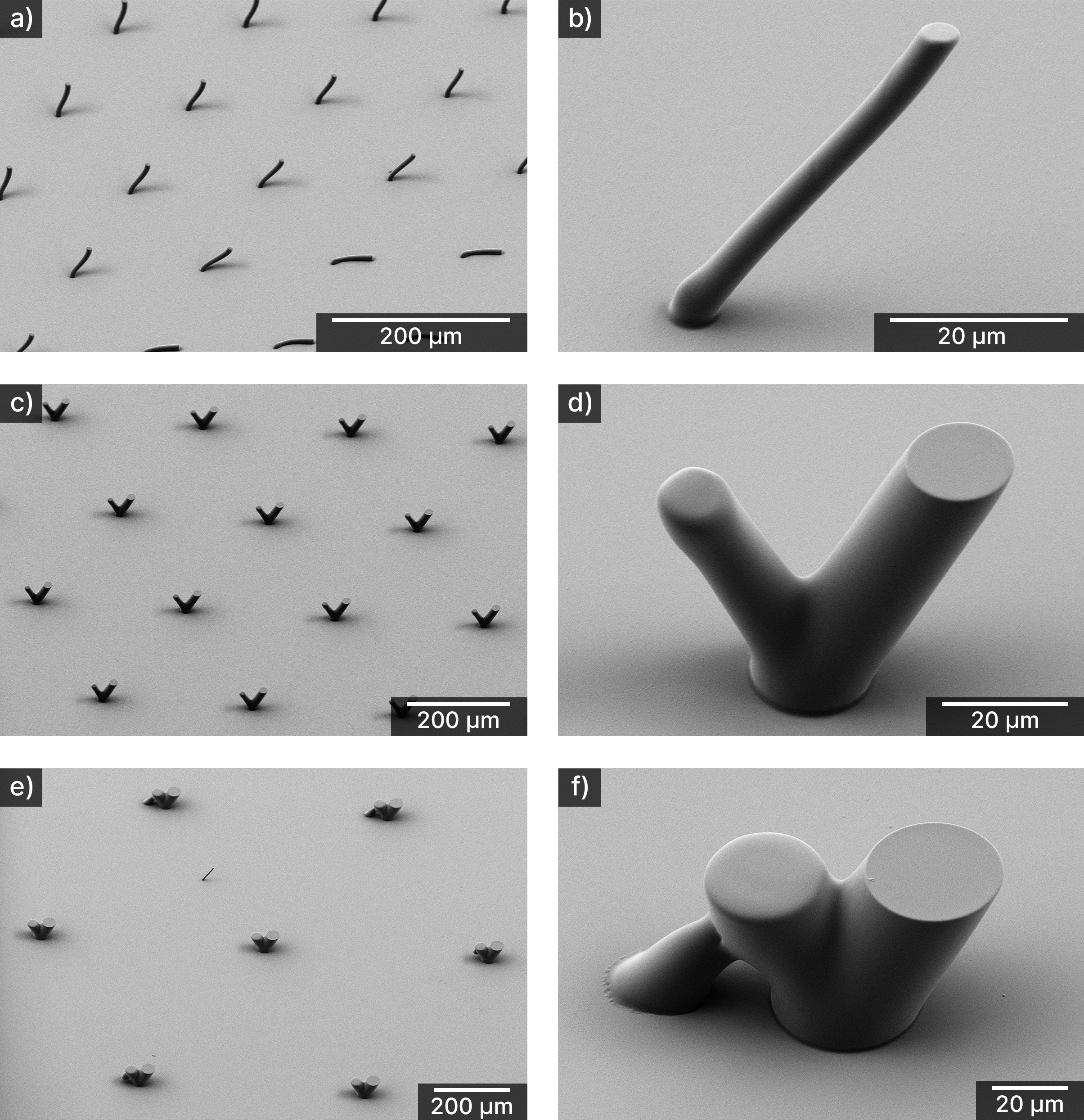 Figure 7: Electron micrographs of 45 µm tall SU-8 features after one inclined exposure step. Features with a diameter smaller than 10 µm were prone to collapse (a), while a few were able to stand, as the 6 µm diameter pillar in b). Larger features were more affected by reflection than the smaller ones. UV reflection in the Si substrate and chromium mask resulted in V-shapes of features with 20 µm diameter (c, d) and N-shapes of features with 40 µm diameter (e, f).
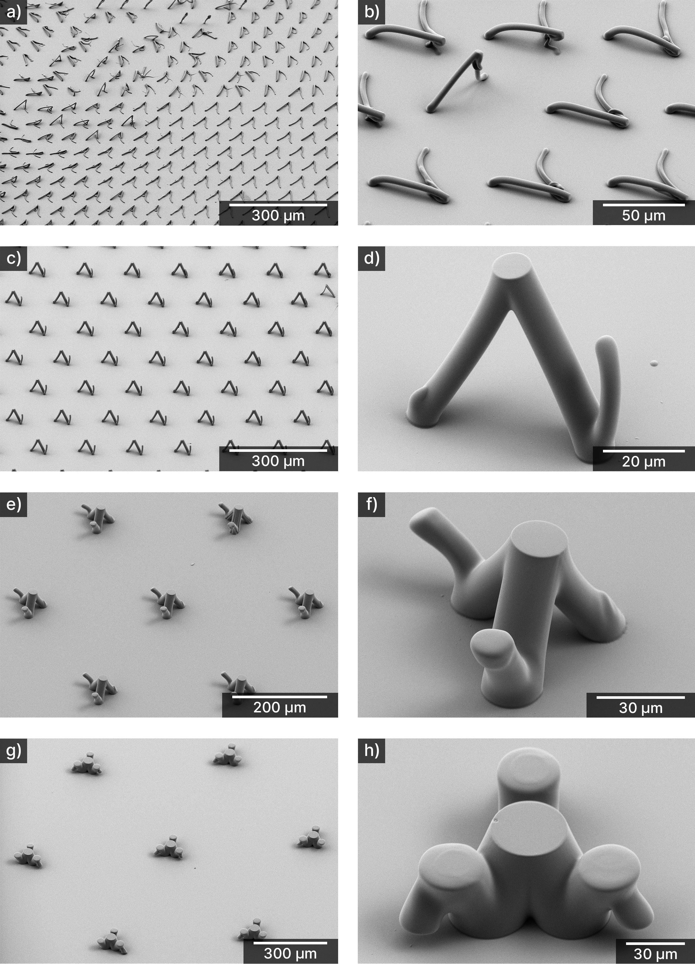 Figure 8: Electron micrographs of 45 µm tall SU-8 features after three exposures from different angles. Features with 5 µm (a, b) and 10 µm (c, d) diameter are inexplicably missing a leg. As for the one step exposure, significant reflection can be seen here as well, most noticeable for 10 µm, 20 µm (e, f) and 40 µm (g, h) diameter features.