6502 architecture - Falmouth-Games-Academy/comp310-wiki GitHub Wiki
Introduction
The 6502 is an 8-bit microprocessor created in 1975. It quickly became popular as it was the cheapest microprocessor on the market, and one of the fastest, at that time 1(https://research.swtch.com/6502). The cost of other processors at the time was around $200, whereas the 6502 cost fraction of that at $25 [9]. Likely because of this, the 6502 and its variants went on to be the standard chip in some of the most iconic electrical devices. Apple II, the Commodore PET, the Commodore 64, and the BBC Micro [9] to name a few. The drastic cost reduction was said to come from a different manufacturing process that yields ten times more usable chips than its competitors.
Even without the cost, the 6502 has several attractions over it's competitors. It has a very simple BUS structure to design and build with, a large stack space which is accessible to developers, extensive documentation, and an assembly language that makes it easy to envision solutions [10]. One developer has said on the 6502.org forum, "Yeah, programming the 6502 is like a guilty pleasure for my brain. It seems to know what I'm trying to say, and it just does it without complaining about the atrocious way I said it." While this author neither endorses nor condemns atrocious code structure, the enormous support and passion from hobbyists and purists for this nostalgia inducing processor is immediately apparent from the tutorials and fan service available. In fact it is still being manufactured and sold today!
The processor is little-endian (although care should be taken developing for the Nintendo Entertainment System (NES) as some registers like the PPUADDR are big-endian 11(http://wilsonminesco.com/6502primer/65tutor_intro.html)), with the ability to handle 64kb of memory at a time 2(http://www.obelisk.me.uk/6502/architecture.html). The general registers that can be directly controlled are A, X and Y. There are other 8 bit registers that can be accessed such as the status register and stack pointer. The program counter is different though being 16 bits wide, this means that the processor can access memory for $0000 to $ffff, this totals to 65536 bytes 3(https://safiire.github.io/blog/2015/03/29/creating-sound-on-the-nes/).
MOS Technologies
The engineers that went onto creating the 6502 first worked for Motorola, but when they were told to stop work on the more affordable microprocessor the group of engineers moved to MOS Technologies 4(https://www.commodore.ca/commodore-history/the-rise-of-mos-technology-the-6502/). In 1976 they built the first single board computer to show the capabilities of the 6502 microprocessor 5(https://www.commodore.ca/commodore-products/productscsg-mos-commodore-kim-1-history-pictures/).

![Figure 1 [6]](https://en.wikipedia.org/wiki/KIM-1#/media/File:Kim-1-computer.jpg)
Architecture
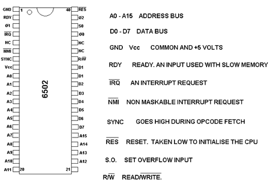
Figure 2 shows the input/ output pins of the 6502 microprocessor.
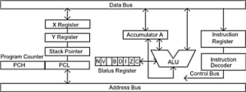
Figure 3 is a basic diagram of the 6502 architecture.
The Arithmetic Logic Unit
The Arithmetic Logic Unit (ALU) is the most important part of the 6502 chip, it is the heart of the CPU. Every time a calculation or logical operation is performed, the ALU where it is processed. The ALU can only perform addition and subtraction operations, however Multiplication and division is possible using different methods. The ALU has two 8 bit input registers (A and B) and one output register. The ALU has five inbuilt operations; ADD, OR, XOR, AND, Shift Right. When two numbers are to be added or compared, one number is fed into register A and the other into register B. The ALU then carries out the calculation and outputs the result on a data bus so it can be transported to wherever it is needed 12(https://twitalu.wordpress.com/2013/06/25/introductions-and-the-6502-alu/) 13(https://www.atariarchives.org/roots/chapter_3.php).

Figure 4 is the design of the ALU
References
-
[3] https://safiire.github.io/blog/2015/03/29/creating-sound-on-the-nes/
-
[4] https://www.commodore.ca/commodore-history/the-rise-of-mos-technology-the-6502/
-
[5] https://www.commodore.ca/commodore-products/productscsg-mos-commodore-kim-1-history-pictures/
-
[6] https://en.wikipedia.org/wiki/KIM-1#/media/File:Kim-1-computer.jpg
-
[7] http://www.hobbyprojects.com/microprocessor_systems/6502_CPU.html
-
[8] http://bucarotechelp.com/computers/architecture/82112201.asp
-
[12] https://twitalu.wordpress.com/2013/06/25/introductions-and-the-6502-alu/