Architecture Overview - wgrzegorz/c5xtools GitHub Wiki
Normative source: SPRU056D, chapter 2 (Architectural Overview). This page summarizes the TMS320C5x bus structure, CPU, on-chip memory, on-chip peripherals, and the test/emulation logic at a block level.
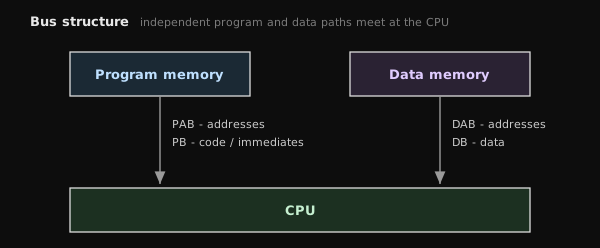
The 'C5x keeps program and data on separate buses, which lets the device fetch an instruction and move an operand at the same time. This Harvard-style separation is what makes the single-cycle multiply/accumulate possible: the multiplier can be fed a coefficient over one bus and a sample over another in the same machine cycle. On top of that parallelism the device carries its own control logic for interrupts, repeated instructions, and subroutine calls.
flowchart TB
    subgraph CPU
        CALU[CALU: 16x16 mult, PREG,<br/>32-bit ALU, ACC, ACCB, shifters]
        PLU[PLU]
        ARAU[ARAU: AR0-AR7, INDX, ARCR]
        MMR[Memory-mapped registers]
        PC[Program controller]
    end
    subgraph MEM[On-chip memory]
        ROM[Program ROM]
        DARAM[DARAM B0/B1/B2]
        SARAM[SARAM]
    end
    subgraph PER[On-chip peripherals]
        CLK[Clock generator]
        TMR[Timer]
        WS[Wait-state generators]
        IO[Parallel I/O ports]
        SER[Serial ports]
    end
    CPU --- PB[Program bus PB / PAB]
    CPU --- DBUS[Data read bus DB / DAB]
    PB --- MEM
    DBUS --- MEM
    CPU --- PER
    JTAG[JTAG / analysis block] --- CPU
The architecture is built around four major buses:
| Bus | Abbreviation | Role |
|---|---|---|
| Program bus | PB | Carries instruction codes and immediate operands from program memory space to the CPU |
| Program address bus | PAB | Supplies addresses to program memory space, for both reads and writes |
| Data read bus | DB | Connects CPU elements to data memory space |
| Data read address bus | DAB | Supplies data-memory addresses |
Because the program and data paths are independent, they can cooperate: one transfer can bring an operand from on-chip data memory while another brings a value from internal or external program memory, delivering both to the multiplier for a single-cycle multiply/accumulate. The same parallelism lets a set of arithmetic, logic, and bit-manipulation operations complete in one machine cycle.
The CPU is made of five building blocks:
- Central arithmetic logic unit (CALU)
- Parallel logic unit (PLU)
- Auxiliary register arithmetic unit (ARAU)
- Memory-mapped registers
- Program controller
The CPU keeps source-code compatibility with the earlier 'C1x and 'C2x generations while adding capability: a 32-bit accumulator buffer, extra scaling, new instructions, and block-move and memory-mapped-register instructions for data management.
The CALU performs 2s-complement arithmetic and contains:
| Element | Width |
|---|---|
| Multiplier | 16-bit by 16-bit |
| Arithmetic logic unit (ALU) | 32-bit |
| Accumulator (ACC) | 32-bit |
| Accumulator buffer (ACCB) | 32-bit |
| Output shifters | at the outputs of both the accumulator and the product register (PREG) |
The multiplier feeds the product register PREG; shifters at the ACC and PREG outputs provide the additional scaling mentioned above.
The PLU is an independent unit that runs in parallel with the ALU. It handles Boolean operations and the bit manipulation that controllers need: it can set, clear, test, or toggle bits in a status register, a control register, or any data-memory location. It reads and writes the data-memory value directly and writes the result back to that same location, without disturbing the ACC or PREG.
The ARAU is an unsigned 16-bit arithmetic unit that computes indirect addresses. Its inputs are the auxiliary registers (AR0 to AR7), the index register (INDX), and the auxiliary register compare register (ARCR). It can autoindex the current AR while a data-memory location is being addressed, stepping either by 1 or by the contents of INDX. Because the ARAU does this address arithmetic, the CALU is left free for other work in parallel.
The 'C5x maps 96 registers into page 0 of data memory space. Every 'C5x device has 28 CPU registers and 16 I/O port registers; the number of peripheral and reserved registers varies by device. Since these registers live in data memory space, software reads and writes them like any other data-memory location. They serve as indirect address pointers, temporary storage, CPU status and control, and operands for integer arithmetic through the ARAU.
The program controller decodes instructions, manages the CPU pipeline, holds the status of CPU operations, and decodes conditional operations. The architecture's parallelism lets the device carry out three memory operations in one machine cycle: fetch an instruction, read an operand, and write an operand. The controller is built from:
- Program counter
- Status and control registers
- Hardware stack
- Address generation logic
- Instruction register
The 'C5x carries three kinds of on-chip memory:
- Program read-only memory (ROM)
- Data/program dual-access RAM (DARAM)
- Data/program single-access RAM (SARAM)
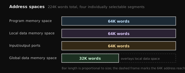
The device has a total address range of 224K words by 16 bits, split into four individually selectable segments:
Every 'C5x device carries a 16-bit on-chip maskable programmable ROM (sizes vary by device). It is used to boot program code from slower external ROM or EPROM into fast on-chip or external RAM. The 'C50 and 'C57S have boot-loader code resident in this ROM; on the other devices the boot loader is an option. The on-chip ROM is selected at reset by driving the MP/MC pin low; if it is not selected, the device starts executing from off-chip memory. After a custom program has been booted into RAM, the boot ROM can be removed from program memory space by setting the MP/MC bit in the processor mode status register (PMST). The ROM is otherwise intended to hold the user's finished program, which is submitted to Texas Instruments for implementation into the device.
Every 'C5x device carries 1056 words by 16 bits of on-chip dual-access RAM, divided into three selectable blocks:
| Block | Size | Configurable as |
|---|---|---|
| B0 | 512 words | data or program memory (by software) |
| B1 | 512 words | data memory only |
| B2 | 32 words | data memory only |
DARAM is mainly intended for data but can also hold programs. The whole array can be configured either as 1056 words of data memory, or as 544 words of data memory plus 512 words of program memory (that is, with B0 switched to program). DARAM speeds up the CPU, which runs a 4-deep pipeline that reads data in the third stage and writes in the fourth: the two data buses (DB and DAB) let the CPU read from and write to DARAM in the same machine cycle, so one instruction can read while the previous one writes.
Every 'C5x device except the 'C52 carries on-chip single-access RAM of various sizes. Code can be booted from off-chip ROM into SARAM and then run at full speed. Software can configure SARAM in one of three ways:
- All of it as data memory
- All of it as program memory
- Part as data and part as program memory
SARAM is organized as 1K- and/or 2K-word blocks that are contiguous in the address space. The CPU can access different SARAM blocks in parallel, but any one block can be accessed only once per machine cycle: the CPU can read or write one block while accessing another. When the CPU asks for multiple accesses to a single block, SARAM returns a not-ready condition and serializes the accesses one cycle at a time. SARAM is more flexible than DARAM in address mapping because it can be mapped into both program and data space at once; the trade-off is that an instruction fetch plus a data fetch that would take one cycle in DARAM may take two in SARAM.
The 'C5x devices offer a maskable option that protects on-chip memory contents. When the related bit is set, no externally originating instruction can access the on-chip memory spaces.
All 'C5x devices share the same CPU, but differ in the peripherals attached to it. The available peripherals are:
- Clock generator
- Hardware timer
- Software-programmable wait-state generators
- Parallel I/O ports
- Host port interface (HPI)
- Serial port
- Buffered serial port (BSP)
- Time-division multiplexed (TDM) serial port
- User-maskable interrupts
The clock generator pairs an internal oscillator with a phase-locked loop (PLL). It can be driven by a crystal resonator circuit or by an external clock source. The PLL can multiply the clock source by a set factor to produce the internal CPU clock, so the source frequency can be lower than the CPU frequency.
A 16-bit hardware timer with a 4-bit prescaler is provided. Its rate is between 1/2 and 1/32 of the machine cycle rate (CLKOUT1), depending on the divide-down ratio. Status bits can stop, restart, reset, or disable it.
The device can generate wait states for slower off-chip memory and I/O without external hardware. The logic is a set of wait-state generating circuits, each individually programmable for a different number of wait states on off-chip accesses.
A total of 64K I/O ports are available; sixteen of them are memory-mapped into data memory space. Any I/O port can be addressed with the IN or OUT instruction, and the memory-mapped ports can also be reached with any instruction that reads or writes data memory. The IS signal marks an I/O read or write. This lets the device interface with external I/O devices with minimal off-chip address decoding.
The HPI, available on the 'C57S and 'LC57, is an 8-bit parallel I/O port that connects to a host processor. The DSP and the host exchange information through on-chip memory that both can access.
Three kinds of serial port exist: a general-purpose serial port, a TDM serial port, and a buffered serial port. Each 'C5x has at least one general-purpose, high-speed, synchronous, full-duplex serial port for talking to codecs, serial A/D converters, and similar devices.
| Port | Where | Notes |
|---|---|---|
| General-purpose serial port | all 'C5x devices (at least one) | Up to 1/4 the machine cycle rate (CLKOUT1); transmitter and receiver double-buffered and individually controlled by maskable external interrupts; data framed as bytes or words |
| Buffered serial port (BSP) | 'C56 and 'C57 devices | Full-duplex, double-buffered, with an autobuffering unit (ABU) for high-speed transfer and lower interrupt latency; flexible data-stream length |
| TDM serial port | 'C50, 'C51, 'C53 devices | Full-duplex; software-configurable for synchronous or time-division multiplexed operation; common in multiprocessor designs |
The count and type of serial and parallel ports per device and package are given in SPRU056D Table 2-1.
Four external interrupt lines (INT1 to INT4) and five internal interrupts (a timer interrupt and four serial-port interrupts) are user maskable. When an interrupt service routine runs, the program counter is saved on an 8-level hardware stack and the contents of eleven specific CPU registers are automatically shadowed on a 1-level-deep stack; a return-from-interrupt instruction restores those registers.
The 'C5x uses an IEEE Standard 1149.1 (JTAG) interface for emulation and test. Two variants exist:
- With boundary scan, on the 'C50, 'LC50, 'C51, 'LC51, 'C53, 'LC53, 'C57S, and 'LC57S. The boundary scan reaches the interfacing devices and can test pin-to-pin continuity and run operational tests on devices peripheral to the 'C5x.
- Without boundary scan, on the 'C52, 'LC52, 'C53S, 'LC53S, 'LC56, and 'LC57. Here JTAG is used for emulation only, interfacing to internal scanning logic that reaches all on-chip resources, so the device supports on-board emulation through the serial scan pins and the emulation-dedicated pins.
An on-chip analysis block, working with the 'C5x debugger software, provides debugging and performance evaluation in a target system. The full analysis block offers:
| Capability | Details |
|---|---|
| Flexible breakpoints | Triggered on program fetches/reads/writes, EMU0/1 pin activity, data reads/writes, CPU events (calls, returns, interrupts/traps, branches, pipeline clock), or event-counter overflow |
| Performance event counting | CPU clocks, pipeline advances, instruction fetches, calls/returns/interrupts/traps/branches, program fetches/reads/writes, data reads/writes |
| PC discontinuity trace | A trace buffer that monitors program counter flow |
A reduced analysis block, on the 'C53S and 'LC53S, supports breakpoint triggering on program fetches/reads/writes and EMU0/1 pin activity only.
The JTAG interface, boundary-scan capability, and analysis-block configuration per device are listed in SPRU056D Table 2-2.
MIT - (c) 2026 Grzegorz Worona [email protected]. See LICENSE.