Header Pinouts - v3l0c1r4pt0r/lkv-wiki GitHub Wiki
J4
| No | Function | MU1 pin | U2 pin | U3 pin | Notes |
|---|---|---|---|---|---|
| 1 | RX | 65GPIO28 | NC | UART output | |
| 2 | GND | ||||
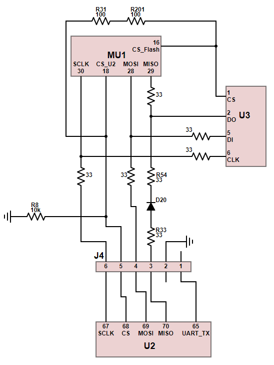
| 3 | SPI MISO | 29ND1 | 70GPIO3 | 2DO | J4.3 is directly connected to U2.70. The connection from J4.3/U2.70 to MU1.29/U3.2 goes through R33, D20, R54 |
| 4 | SPI MOSI | 28ND0 | 69GPIO2 | 5DI | |
| 5 | SPI CS# | 18GPIO19 | 68GPIO1 | This CS and the CS used for MU1->U3 communication (MU1.16, U3.1) are tied together with 200 ohms (R31, R201). Both CS are also pulled down with a 10K resistor (R8), so they are active by default when the board powers up. | |
| 6 | SPI SCLK | 30ND2 | 67GPIO0 | 6CLK |
J6
| No | Connection |
|---|---|
| 1 | MU1 pin 24 (GPIO10) |
| 2 | GND |
Unmarked 2-pin header near U4
| No | Connection |
|---|---|
| 1 | U2 pin 125 (GPIO15 = BOOT_CFG1). Pulled down to GND with 10k resistor. |
| 2 | 1k resistor to VCC |
SW2
SW2 is not populated, but 10k pulldown resistors are populated on the bottom of the board for each switch
| No | MU1 pin | MU1 pin name |
|---|---|---|
| 1 | 39 | LD14 |
| 2 | 40 | LD15 |
| 3 | 41 | LD16 |
| 4 | 42 | LD17 |
| 5 | 43 | LD22 |
| 6 | 44 | LD23 |