Home - tvelliott/jPCBSim GitHub Wiki
2018-09-15 Update
New features:
Simulations for N-port (up to 9 ports) touchstone output now supported. Use TP1, TP2, TP3,... TP9. Anything >2 ports, uses the touchstone N-port format. TP1 is always the excitation port.
Re-enabled LorentzMaterials for the pcb dielectric. Requires a patch to newest version of openEMS. You can follow the instructions for building openEMS, but build from the local fork for now. A pull-request has been submitted.
https://github.com/tvelliott/openEMS-Project (local fork with fix)
Coming soon... examples including validation via measurements
Introduction
The goal of the jPCBSim application is to improve a users ability to maintain, configure, and simulate planar pcb-based filters, antennas, and other 1-port / 2-port devices using the openEMS FDTD engine. Octave and gnuplot (current interfaces for openEMS) are not required to simulate pcb structures with jPCBSim. The first step is to create a 2-layer pcb using EagleCad. Currently, excitation and sensor ports are positioned by placing smd test pads (from testpad.lbr) with the device names TP1 (excitation) and TP2 on the port areas of the pcb design. These pads are converted to box-type lumped element ports with a user-defined termination resistance. The ports extend from the top copper to the bottom copper with the ends matching the dimension of the test pads. The pcb is then exported from eaglecad using the hyperlynx ulp script. A .hyp file is then imported (via the hyp2mat software). jPCBSim is then used to configure various parameters to be simulated. The output generated by jPCBSim is an xml file that is structured in a format that openEMS reads for simulation. The time-domain data output from openEMS is output in steps throughout the entire simulation. jPCBSim reads this data during the simulation on a user-defined interval and converts it to frequency domain via FFT. The complex values returned are used to generate s-parameter plots s11/s21, smith chart plot of s11, and touchstone outputs .s1p for 1-port, .s2p for 2-port device. The touchstone outputs can be imported into a circuit simulator such as QUCS where the PCB can now be inserted into an s-parameter circuit simulation just like any other 1-port / 2-port device. E-field dumps can be enabled, allowing the user to view animated e-field propagation along the surface plane of the pcb with paraview software.
Features
-Written in Java, Utilizes Jogl (openGL bindings), Same executable runs on Windows and Linux.
-Generates output that can be directly solved with the openEMS FDTD field solver
-Graphically manage simulation parameters configurations for multiple projects.
-Microstrip calculator aids in converting to/from lumped element / distributed elements
-1 and 2 port planar (e.g. microstrip) pcb devices can be designed using eagle cad pcb design software. Currently, only Gaussian excitation with lumped element terminations are supported.
-pcb thickness can be re-scaled upon import from eagle cad / hyperlynx / hyp2mat conversion.
-easy mesh generation. automatic in most cases.
-post processing converts time-domain output from the field solver to frequency domain via FFT. Currently, output includes s-parameter plots s11,s21. Annotated Smith chart generation, and Touchstone s1p and s2p output for import to a circuit simulator such as QUCS. The outputs are generated on a user-programmable period throughout the entire simulation. The user can monitor and decide if the simulation should be aborted early for modifications.
jPCBSim Screen Shots
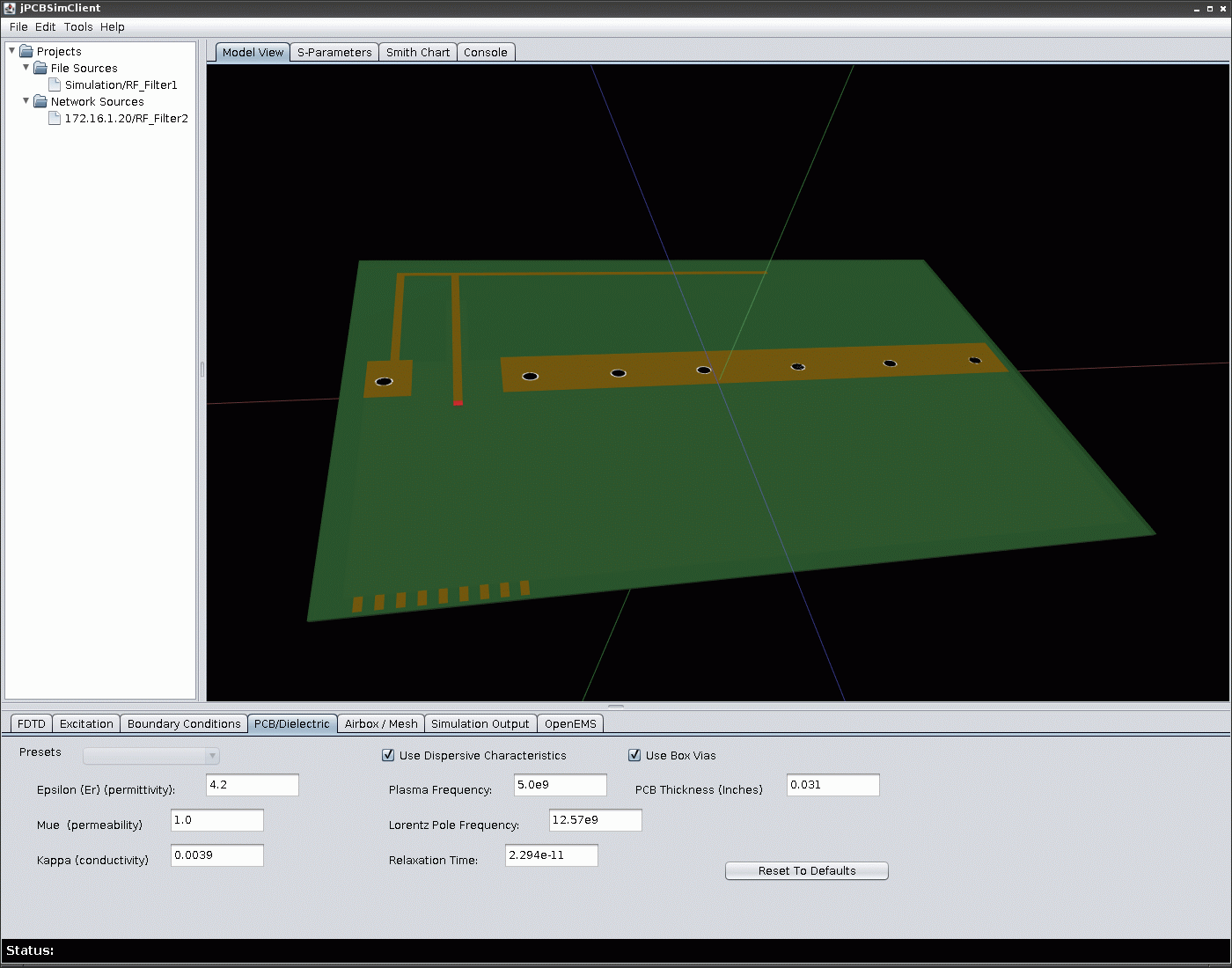 Inverted-F Antenna Example (Top)
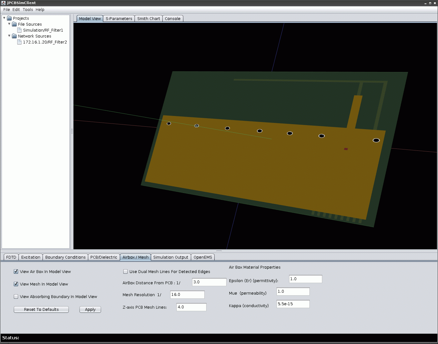 Inverted-F Antenna Example (Bottom)
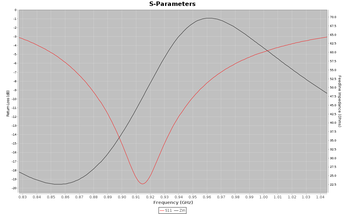 Inverted-F Antenna Example (S-Parameter plot S11)
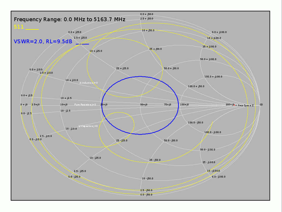 Inverted-F Antenna Example (Smith Chart plot S11)
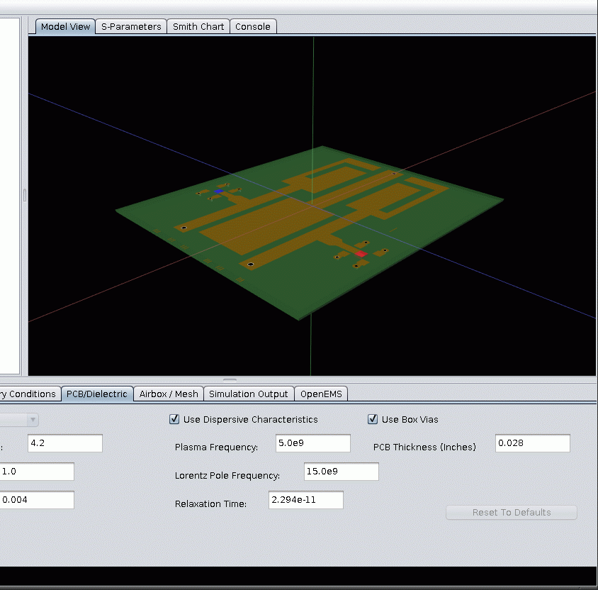
BPF Filter
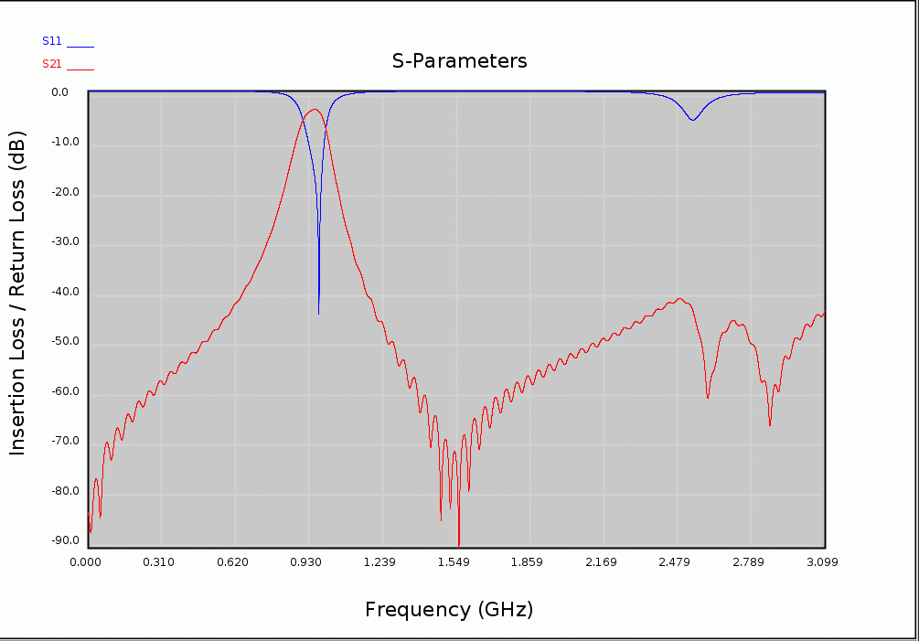
BPF Filter (S-parameter)
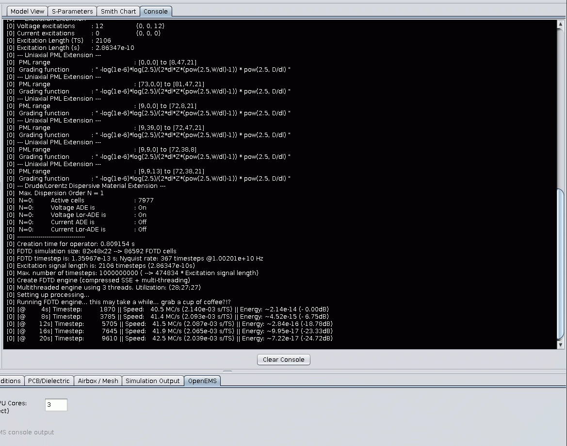
Output from openEMS simulation is displayed on the console during a simulation