Build Notes 2.0beta2 - softerhardware/Hermes-Lite2 GitHub Wiki
DEPRECATED PAGE!!!!
This page is deprecated and kept only for historical reference. There have been many changes since beta2. Please see the Hermes-Lite 2.0 Getting Started for current details.
Build Notes 2.0beta2
These are notes to help those building the Hermes-Lite 2.0beta2 printed circuit board by hand.
Schematics
You can find the latest Hermes-Lite 2.0 schematics on www.hermeslite.com. For a Hermes-Lite 2.0beta build, please be sure you are using a schematic that says "Rev: 2.0beta2" in the lower right corner.
The schematic component prefix "DB" is used for any connector intended for a daughter board. These should only be stuffed as needed.
The schematic component prefix "B" is used for 0.1uF capacitors.
Sometimes it can be confusing finding schematic component's footprint on the PCB. The best way to do this is to use KiCAD. The KiCAD files can be found here. It is easiest to just clone or create a zip file of the Hermes-Lite2 project directly from github. Also, enlarged PDFs of the front silkscreen and back silkscreen are also available.
BOM
Hermes-Lite 2.0beta2 builders must procure all required parts on their own. There are two build options:
- Standard which includes QRP PA, digital bias, TR relay, low power RF/PA switch, high current 9V supply and instrumentation slow ADC
- No PA which only includes low power RF output
You can find both BOMs here. Please be sure that the BOM says 2.0beta2 at the top of the first page.
The BOMs include links to Mouser or Digi-Key sources for the part line items. There also may be group members who have created sharable shopping carts. Please check the Hermes-Lite Google Group for the latest details.
At the end of the BOM is a list of all components that should be omitted in your build. It may be helpful to go over this list and cross out these components on your printout of the schematics.
It can be helpful to build a Hermes-Lite 2.0 by blocks where each block is tested as it is completed. The schematic pages are grouped into such blocks.
Power Supply
The power supply schematic page contains the title "Power" in the lower right corner. The components on this page can be assembled first.
Option: Low or High Current 9V Supply for Driver
In standard builds using the onboard AFT05MS003 QRP PA, the PA shares a high current 9V power with the driver. This is U8 and the surrounding components. For this option, J6 must remain open but J20 must be shorted.
In no PA builds or PA builds that use a final LDMOS device using 12V or higher, a lower current 10V supply is provided for the driver. This is U12 and the surrounding components. For this option, J6 must be shorted and J20 must be open.
Option: LVDS and Ethernet Bank Voltages
The ethernet interface or LVDS IO pins may be set to 2.5 or 3.3 V logic. This is done by selecting FB27 or FB28 and FB29 or FB30 for installation. To reduce current consumption and noise, please select 2.5V for all builds. This is what has been tested so far. Be very careful not to install both ferrite beads as that will short your 3.3V and 2.5V supplies together!
Option: Switching Power Supply Synchronied by FPGA
There is an option for the FPGA to generate the switching power supply clocks. This is to provide a mechanism to move any spurs possibly created by the power supply. For now, the gateware is not using this option. J2, J11 and J19 must be shorted. R13, R16 and R47 may be left open.
Issues and Required Modifications
The connector CN2 has a dual purpose footprint to support a terminal block connector or power pole connector. The power pole connector holes are too small on the 2.0 beta2 boards so only the terminal block connector is supported. You may also solder wires directly to the power input connections.
Some early versions of the schematics have the values of R14 and R15 swapped. R14, the resistor in parallel with C19, must be 10K. R15 must be 20K.
Some early version of the BOM specify a part for U1 with the wrong width. This EEPROM must be 3.9mm or 150 mils wide. For example, manufacturer part number S25FL116K0XMFI041 should work.
VPA+ is currently set to 9.44V. This may be slighly high for SWR ruggedness of the AFT05MS003 transistors in the PA. I have recently lowered this to just below 9V by replacing R46 with 1.5K and 75 Ohm resistors in series for 1.575K total. Other standard values of R19 and R46 that should produce near 9V are 16.2K/1580Ohm, 16.9K/1650Ohm, 17.8K/1740Ohm, 15.8K/1540Ohm and 15.4K/1500Ohm.
Testing
Before powering up, check that there are no shorts between the 1.2V, 2.5V, 3.3V, VPA+ and external power input with an Ohm meter. Also use an Ohm meter to check that there is continuity to the proper power supply through all installed ferrite beads.
Connect a 11 to 15V power supply and measure that the voltages produced are correct. DB9, DB12 and DB14 may be used to measure 3.3, 1.2 and 9V respectively. Measure 2.5V at the terminal of C25.
FPGA
There is no single schematic sheet for the FPGA, but once the power supply is verified working, the FPGA may be installed. Also, please install FPGA LEDs D2,D3,D4,D5 and R74,R73,R72,R71 found on the schematic "Hermes-Lite Input Ouput" to use as test indicators.
Options
There are currently no options for the FPGA build.
Issues and Required Modifications
There are no issues or required modifications for the FPGA build.
The FPGA LEDs are very bright. The resistance of R71-R74 may be increased.
Testing
Download the .jic LED test bitfile found here to test initial life of the FPGA. First connect your Altera Blaster to CN1. Align the key on the Altera blaster plug with the silkscreen for CN1 on the PCB. The gateware download procedure is as described on the Hermes-Lite 1.22 Firmware Wiki.
This test is successful if the programming process completes and 2 of the 4 LEDs are lit.
Ethernet
Proceed to install all components on the schematic sheet titled "Ethernet." It helps to install the MagJack, CN3, last as it can block access to some of the other smaller components. CN3 also prevents the PCB from laying flat. I installed standoffs in the four mounting holes so that I could lay the PCB flat on either side.
Options
In the future, J1 may be omitted to provide an extra free FPGA IO pin. For now, please install J1 as the current gateware senses when the ethernet PHY is out of reset.
Issues and Required Modifications
The LEDs on the jack are dim. The values of R30 and R31 are set for 3.3V Veth but we are running at 2.5V. 220 or 250 Ohm resistors may be substituted. Care must be taken as we have a limited current budget for the 2.5V supply. More experimentation is required.
Only gigabit ethernet is currently supported. Future plans are to be able to switch fromm 1000Mb/s to 100Mb/s ethernet.
Testing
Using the same leds.jic bitfile as used for the FPGA test, you should see the 4 LEDs (D2,D3,D4,D5) count in binary. This confirms that the clock generated by the Ethernet PHY is reaching the FPGA.
Once the Ethernet PHY clock is confirmed, connect the HL2 to gigabit ethernet and download the ethernet test gateware to the FPGA. The HL2 should receive an IP address via DHCP and you should be able to ping your HL2.
Clock
Install all the required components in the BOM for the schematic sheet titled "Clock." The oscillator specified in the BOM is tricky to solder. Make sure the two center pads of the oscillator are not connected to one of the four outside pins. I used hot air to solder this.
Option: No Versa Clock
Future builds may leave the entire clock circuitry off and instead populate X3 on the RF Frontend schematic. This will require changes to the gateware as the AD9866 must now double the clock frequency. Also, use of the AD9866 PLL may result in higher clock phase noise as discussed here. This option is not recommended for early builds.
Option: Crystal for X2
There is an option to use a crystal for X2 instead of an oscillator. This can reduce costs. The Versa5 chip also has digitally programmable capacitors for a crystal so the frequency can be shifted without VCO. This option is not recommended for early builds.
Option: VCO for X2
An alternate oscillator for X2 is a VCO. This requires the MCP4716 DAC to set the VCO voltage. This option is not yet supported in the gateware.
Option: Bypass Versa5
Wires may be run from the oscillator directly to the RFFE_CLK to bypass the Versa5. This is not recommended for early builds.
Option: External Clock
CL1 may be populated to support using an external synchronized clock. CL2 may be populated to drive and become another unit's external clock. This is for experiments with multiple synchronous transceivers. Firmware does not yet support this.
Option: Recovered Clock
For LVDS communication, a recovered clock from the datastream may be used as a synchronous reference clock. This requires including J23 and J5. Firmware does not yet support this.
Option: External I2C
DB1 may be populated to support attaching additional I2C devices.
Issues and Required Modifications
None.
Testing
The test bitfile found here should be downloaded to the FPGA. This will enable the Versa5 and set the proper PLL multiply and divide values. With a scope, you should see a 76.8 MHz digital clock on one pad of J22.
RF Frontend RX
Install the components specified in the BOM for schematic page "RF Frontend" except for the TX components beginning at U7 pins 51,52 and continuing to RF1.
Option: Local Clock
J22 may be excluded and X3,C58,C59 included for a local inexpensive oscillator directly connected to U7. This may result in increased phase noise. It requires changes to the gateware. It is not an option currently supported by the gateware.
Option: External Clock
J22 may be excluded and CL4 included for an external oscillator directly connected to U7. This is to support synchronized receivers in the same case. One master unit produces the clock. The master unit CL2 is connected to the slave unit CL4. This option is not currently supported in the gateware.
Option: Reverse Polatiry of T2
Some commercial baluns have the polarity of T2 pins 4 and 5 reversed. Jumpers J12, J15, J16 and J21 can be configured to reverse the polarity of T2.
Option: Hand Wound or Commercial T2
The footprint for T2 supports multiple uses. It supports a traditional hand wound BN43-2402 balun as described here or a commercial balun as used in the Hermes-Lite1 v1.42 Frontend. Note that the v1.42 balun does not need polarity reversed.
Option: External RX Filter Board
The reconstruction filter L10,L11,C54,C55,C56,C57 may be left off and an optional RX filter daughter board inserted connecting to DB15 and DB4. This daughter board does not yet exist.
Option: No Reconstruction Filter
The reconstruction filter L10,L11,C54,C55,C56,C57 may be excluded and L10 and L11 stuffed as 0 Ohm resistors. This is to support 6M undersampling reception as well as cases where the RX reconstruction filter will be later in the RX chain.
Option: Secondary RX Input
B82 and RF3 may be included for a secondary RX input.
Issues and Required Modifications
TVS diode D1 may not provide adequate protection and may be updated. From the AD9866 datasheet, the maximum allowed input for the ADC is just over 6V peak to peak. Accounting for the transformer T2, we should be protecting for maximum of about 2.1 to 2.2 V at the antenna input. This TVS diode is not doing that.
Testing
The standard most recent Hermes-Lite2 gateware found here may now be used with various software to test receive.
RF Frontend Low Power TX
Install the components specified in the BOM for the RF driver. These are the components on the schematic page "RF Frontend" from U7 pins 51,52 to RF1. The low power TX balun should be wound as described here.
Option: Instrument TX Only, PA TX Only, or Instrument and PA TX
Depending on whether you want instrument TX, PA TX or both, you must stuff specific components and include jumpers. The details of this options are described directly on the schematic.
Option: Adjust Low Power TX Level
The resistor combination of R52,R54,R61 and R52 help define the load seen when the driver is powering RF1 through the PE4259 switches. The values of R54 and R61 may be changed to increase or descrease the power delivered to RF1.
Option: Bypass RF Driver
The RF driver circuit may be excluded entirely. Daughter board connectors DB3 and DB2 exist for experimenting with alternate drivers.
Option: Improve U9 Thermal Dissipation
The thermal pad underneath U9 extends past the op amp IC boundaries. This allows additional heat sinks (copper braid, tab, etc.) to be soldered near DB2 for improved thermal dissipation. Be sure that U9 and all ICs with thermal pads are adequately connected to the thermal pad on the PCB. Since the Hermes-Lite2 uses a 4-layer board, there is more heat sinking via the PCB than the V1.42 frontend and thermal dissipation does not appear to be an issue.
Issues and Required Modifications
The T1 footprint supports various sizes of commercial 1:1 transformers. We need to find a commercial SMT balun that will handle the expected power. We could possibly use a 1.5:1 as used on the Hermes.
Testing
The standard most recent Hermes-Lite2 gateware found here may now be used with various software to test low power TX. TODO: The posted bitfiles do not yet support TX. You must build your own.
QRP Power Amplifier
Install the components specified in the BOM for the schematic page "Hermes-Lite V2 5W Power Amplifier."
Option: TO-220 LDMOS Devices
Although the power amplifier is designed to support TO-220 devices, the bias circuit in the 2.0 beta2 boards will not go high enough to properly bias these devices. Because of this, only build the AFT05MS003 version.
Option: Various Configurations
The power amplifier circuit attempts to be universal. There are several components marked DNI. The use and need of these components will be determined through experimentation.
Option: Input Attenuator
Input power may be attenuated with proper choice of R94,R97,R98 an R100.
Option: Transistor Adapter Board
The footprints for Q3 and Q4 support small adapter boards for a variety of transistors that are mounted at right angle to the main PCB and abutt to the enclosure side for thermal dissipation. The latest version of these boards are found here but will eventually be moved to the new Hermes-Lite2 github repository.
Issues and Required Modifications
The 5V LP2985 as specified in early BOMs will not work as the 3.3V supplied U15 does not permit inputs with that high of voltage. A LP2985-33DBVR must be used for U14 on the 2.0 beta2 boards. This limits the maximum bias to no more than 3.3V which is not enough to properly bias popular Mitsubishi TO-220 devices. Future revisions will update the bias circuilt to support higher biases.
The footprint for relay K2 on 2.0 beta2 boards is mirrored. To fix this, pins 1 and 12 must be swapped. This can be done by installing K2 at an angle so that pins 1 and 12 can be bent out and jumper wires run to the proper pads or vias connected to those pads. This is shown in the picture below. If you do not intend to enclose the PCB, you may also mount the relay on the bottom of the PCB to effectively mirror all pins.
Setting the bias to 100 mA per transistor is difficult as there is no easy place to measure the current and no way currently for software to easily change the bias voltages. The two wires of T3 connecting to pin hole 3 may be left unconnected at first and an amp meter inserted at this point for measurements. Test software should be available soon to adjust bias voltages. An alternate method to set the bias current by measuring variation in the total current to the Hermes-Lite will be developed. Future revisions of the Hermes-Lite2 will have a method to digitally measure the bias current.
Mounting the AFT05MS003 devices directly to the main beta2 board is an experiment in thermal dissipation. As seen in the photo below, the nut and bolt between Q3 and Q4 pull the PCB down to provide better thermal transfer from the bottom edge of the PCB to the aluminum enclosure. Also, the two bolts in the side of the enclosure (roughly at the same location for mounting TO-220 devices for thermal dissipation) hold a strip of copper that presses down on the tabs of the AFT05MS003 devices and against the ensloure side for additional thermal relief. Further experiments are required to determine if this thermal dissipation is adequate. The fallback is to use the transistor adapter boards bolted directly to the enclosure side.
Initial experiments show that there is too much drive to the AFT05MS003-based amplifier. R94,R97,R98 and R100 will be adjusted based on experimental results to achieve 5W output with full RF driver output.

Testing and Usage
Before using the onboard AFT05MS003-based PA, please make sure that you have:
- Replaced U14 with a 3.3V equivalent, LP2985-33DBVR
- Swapped pins 1 and 12 of relay K2
Currently, the PA may only be used with this modified version of Quisk. This version is for Linux only. All other software will never enable bias to Q3 and Q4. A future plan is to release a secondary program to manage Hermes-Lite 2 specific features separately so that it can still be used with other openHPSDR software.
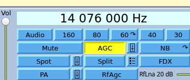
This version of Quisk adds a PA button to the lower left corner of the main window as pictured above. If this button is inactive as pictured above, then the PA is disabled and the lowpower RF is enabled with output on RF1. But if the button is pressed and activated, as shown below, then the lowpower RF is disabled and the PA is enabled with output on relay-switched RF2.
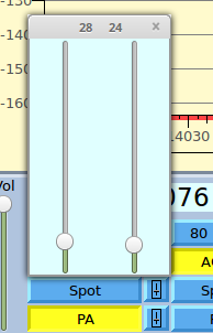
In the picture above, the pop up window with the 2 bias sliders is also shown. This window is opened and closed by pressing the small slider button just to the right of the PA button. The raw potentiometer settings sent to U15 are displayed in the window title. These values range from 0 to 255. The lowest voltage, roughly 0.03V, is seen with a setting of 255. The highest voltage, a few tens of millivolts less than your 3.3V supply, is seen with a setting of 0. Vbias ~= slider_value x .012784 + .03. The left slider sets the bias for Q3, bias0. The right slider is for Q4, bias1.
Each AFT05MS003 requires roughly 100mA of current for proper bias. We can measure this current in several ways:
- Do not solder the centertap of T3 at first, but leave a length of wire. Insert an ammeter and optional current limiting ~5 Ohm resistor between the centertap leads of T3 and pad 2 of T3.
- Insert an ammeter in the main power supply.
Once you are measuring current, connect a dummy load, start Quisk and enable the PA. Ensure that both bias sliders are set to 255, essentially 0V bias. With no microphone input to Quisk or spot value of 0, press PTT on Quisk. Lower one slider until you measure the target current. It is best to take tiny steps with the slider. You can click on the slider then use the up and down arrows on your keyboard to change the value in single increments. You may need to wait 20 to 30 seconds for the bias current to stabilize. Once you have found the setting for one transistor, push that slider back up to 255 and repeat for the other transistor. The setting for each transistor may differ slightly. In the picture, my setting for Q3 is 28 (2.92V) but Q4 is 24 (2.97V).
If you are measuring current through the centertap of T3, the target bias is simply 100 mA for each transistor. If instead you are measuring current at the main power connector, then you must estimate. First, measure a baseline current when PTT is enabled on Quisk (no signal though) and both sliders are at 255. Next, estimate the current change at the power connector for 100mA of bias current:
Idelta = (targetbiascurrent x Vpa)/(powersupplyefficiency x Vexternalpowersupply)
For my HL2 with Vpa at 8.95V, power supply efficiency of roughly 0.9 (see Claudio's measurements), and voltage input of 13.8V, I calculate:
Idelta = 72mA = (0.1 x 8.95)/(0.9 x 13.8)
This is only an estimate. It can be difficult to obtain an accurate efficiency number at low currents. Please update this wiki if you have a better way of doing this. In practice, I measured a change of 50 to 60 mA at the power connector for a bias change of 100 mA. For reference and comparison, my measurements are below.
| Description | Measurement at 13.8V Input |
|---|---|
| RX only | 210mA |
| TX no signal | 220mA |
| TX, Q3 at ~100mA | 280mA |
| TX, Q4 at ~100mA | 275mA |
| TX at 3W | 880mA |
| TX at 5W | 1170mA |
It is easiest to measure the bias voltage at the two vias near pin 1 of DB3.
Once you determine a good bias setting for each transistor, you can have Quisk start with the desired setting by editing your .quisk_conf.py file. See hermes/quisk_conf_hermeslite2.py for examples. There is a new way to save these settings but it is not implemented yet.
Before operating, make sure your transistors are well heat sinked. Also, the PA is currently overdriven and we need to add proper attenuation to the input of the PA. I run Quisk with TX levels of ~20% for 5W output.
Input Output
Hermes-Lite2 schematics dated April 23 2017 or later show connections for CW key in, PTT in, CW out, TX inhibit and Radio ID type on the Input Output page. You may only stuff the components required for those IO blocks. The IO blocks for LVDS and external clock reference do not need to be stuffed as they are not yet enabled.
The PA temperature sensor is enabled. This requires stuffing U13 and U18 as well as surrounding components. Use 0 Ohm resistors or jumpers for D8 and D9. These are not required for the onboard analog channels.