DropBot DB3 120 chips - sci-bots/dropbot-v3 GitHub Wiki
Digital Microfluidic chips for DropBot DB3-120
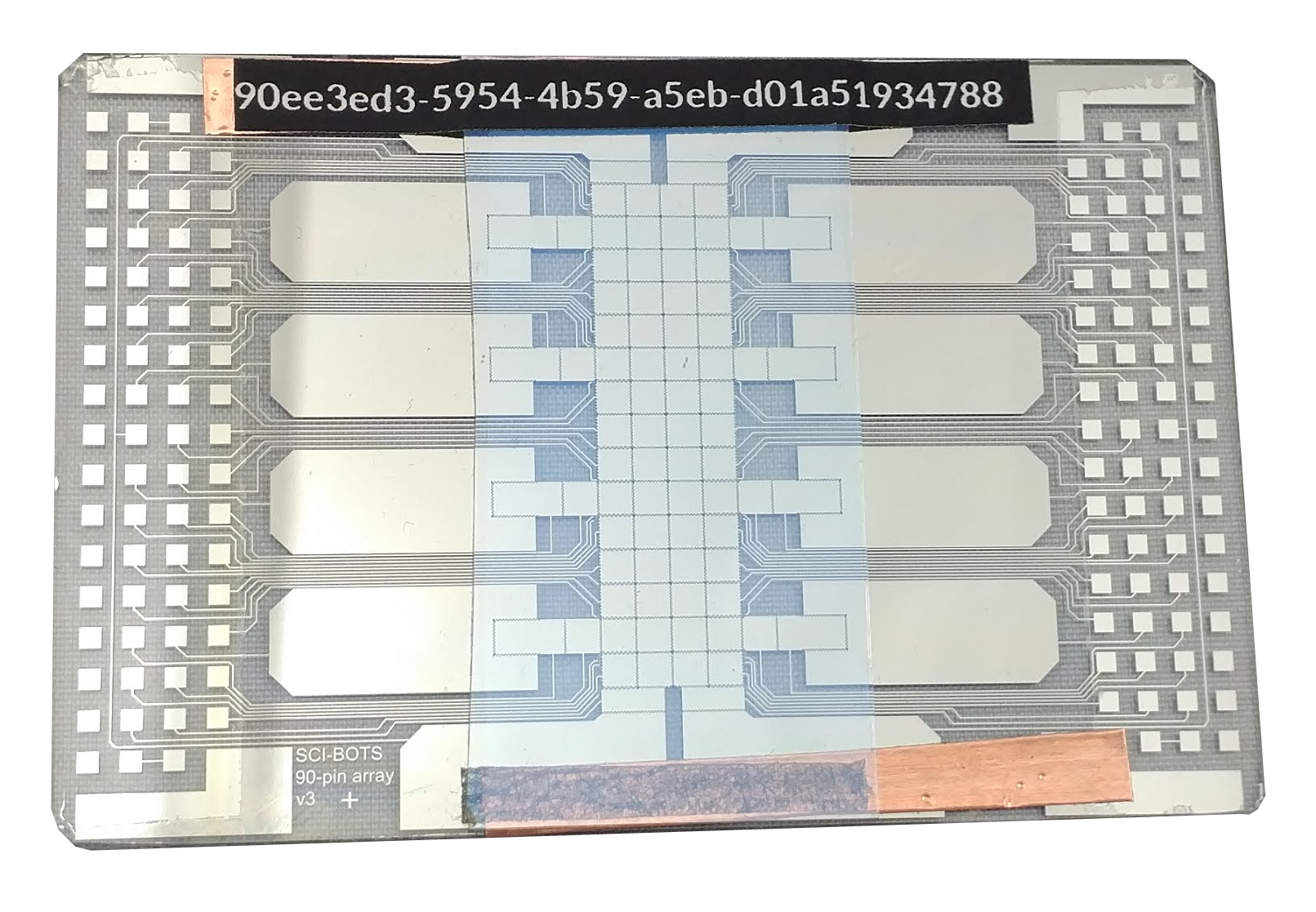
Sci-Bots sells general-purpose, 90-electrode chips for use with the DropBot
DB3-120 system (contact [email protected] for a quote or visit our online store). Our chips are made with the following specifications:
Bottom plate:
- 0.9 mm Soda Lime glass
- High Reflective Chrome electrodes
- Vapour-deposited Parylene-C dielectric coating (6 μm)
- Spin-coated Fluoropel 1101V hydrophobic coating
Top plate:
- 0.7 mm ITO-coated glass (8-12 ohms/sq)
- Spin-coated Fluoropel 1101V hydrophobic coating
There is a 180 um gap height between top and bottom plates
Custom chips
Some users may also be interested in designing custom chips.
Chip design requirements
The main requirements for chips compatible with the DropBot DB3-120 are:
-
Bottom plate MUST be 76.2 mm wide
-
Pogo pin pads MUST match the example mask relative to the front/top edge of the chip (see pin mapping for corresponding channel numbers in the MicroDrop software)
-
Bottom plate MUST be ~1+/-0.2 mm thickness under the pogo pins (top plate may be thicker)
-
Output enable (i.e.,
OE) pad MUST be connected to Ground (i.e.,GND) pad in at least one corner of the chip (see below). It is RECOMMENDED to connectOEtoGNDin all four corners.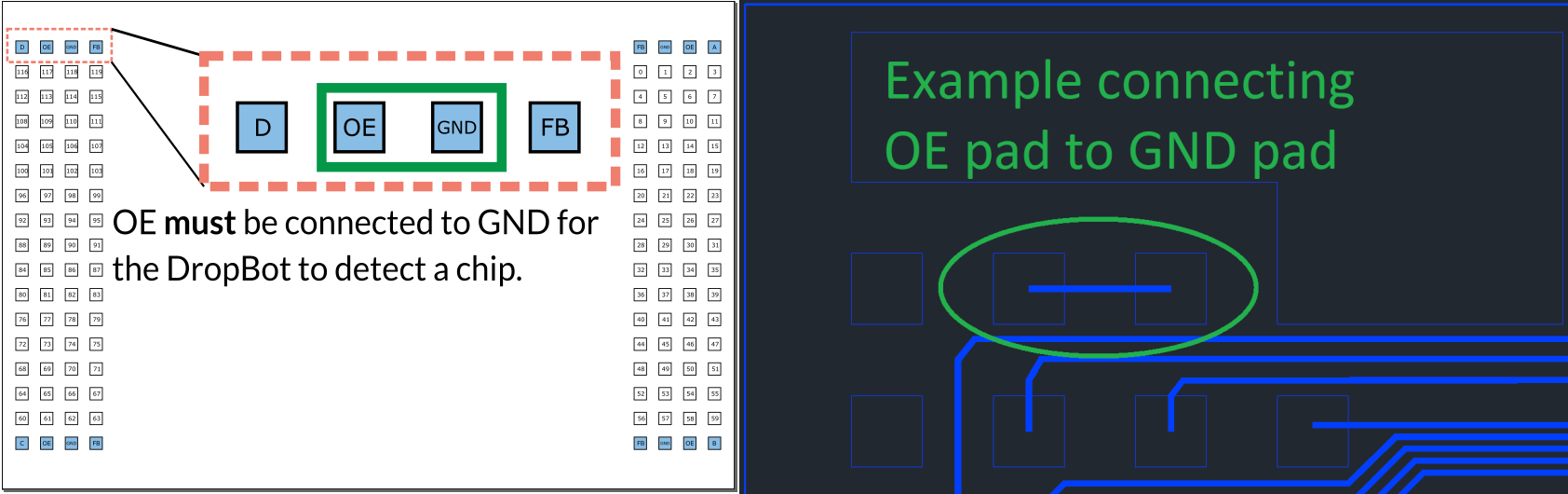
-
For proper DMF operation with the DropBot, the top plate of your device MUST be electrically connected to at least one of the feedback ground pins (i.e.
FB). -
The DropBot chip design template contains an example of electrodes running from the
FBpin to under the top plate that can be easily connected during device assembly using double sided conductive tape:

- The conductive tape (Some examples tapes that work well as a double stack: Copper tape, XYZ Conductive tape) will electrically connect the top plate to the
FBpins while also mechanically holding the top and bottom plates together.
Note: The key words "MUST", "MUST NOT", "REQUIRED", "SHALL", "SHALL NOT", "SHOULD", "SHOULD NOT", "RECOMMENDED", "MAY", and "OPTIONAL" in this document are to be interpreted as described in RFC 2119.
Reference chip design
Here is an example mask (click on image to download in AutoCAD dwg format):
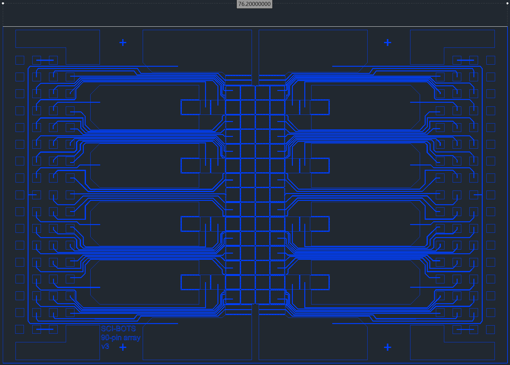
Here is the corresponding mapping of DropBot channels to electrodes on the reference mask:

Please contact [email protected] for more information.