Designing your own Adapters - sanni/cartreader GitHub Wiki
To design your own adapters you need to download and install the following software:
- KiCad
- FreeRouting V1.2.43 (Source code and newer releases that might still be buggy can be found here)
- a Java Runtime Enviroment like OpenJDK
Making an adapter PCB will take you about three hours.
Important: This tutorial will not teach you how to use KiCad, you already need to know how Kicad works. It will just show you how I designed the adapters. To learn KiCad it's best to watch some Youtube videos about KiCad.
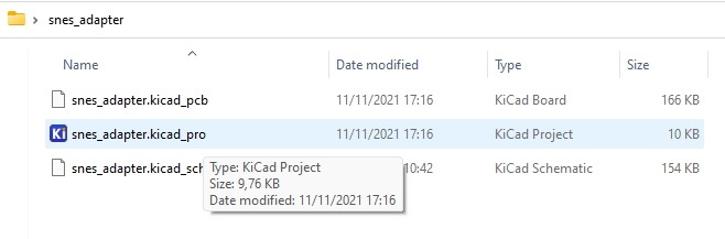
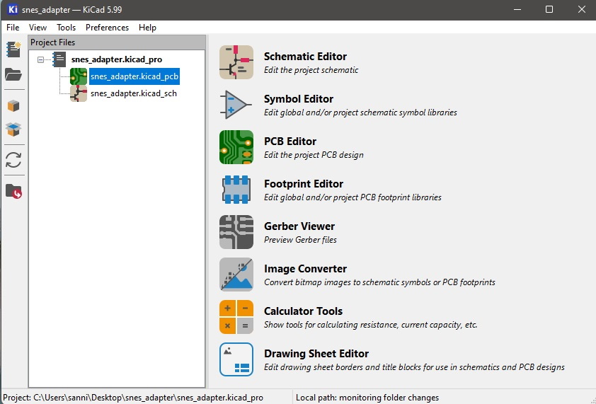
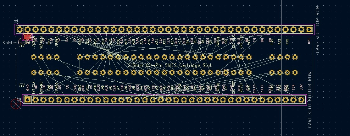
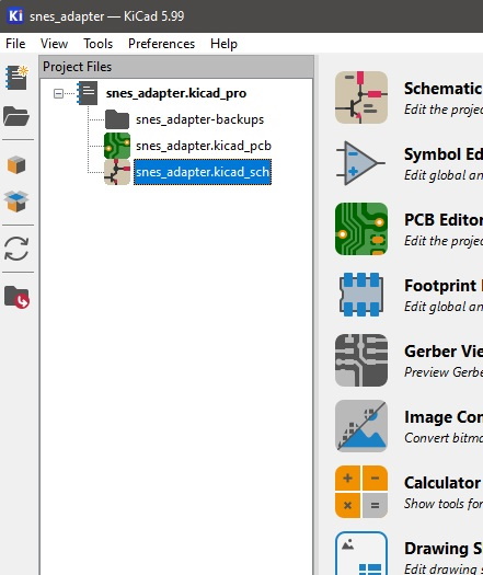
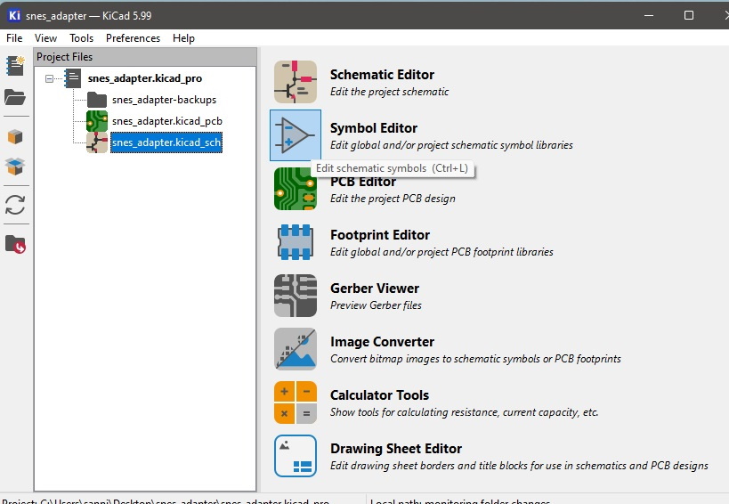
To start download and open the KiCad project of an already released adapter that fits your new adapter idea the best: https://github.com/sanni/cartreader/tree/master/hardware
Double-click on the kicad_pcb file
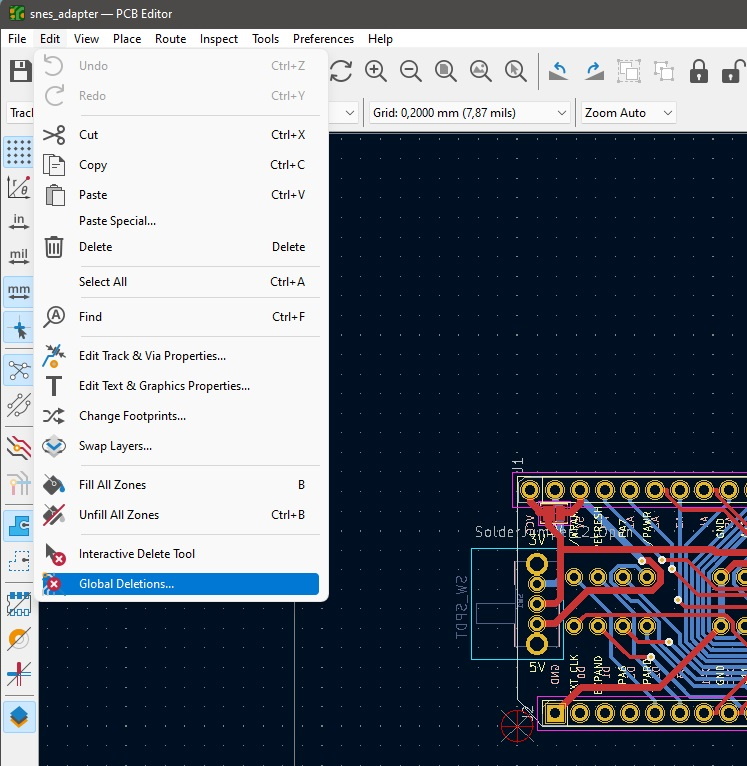
Select Global Deletion to get rid of all the traces
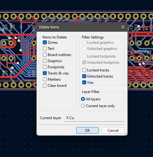
Delete everything you don't need
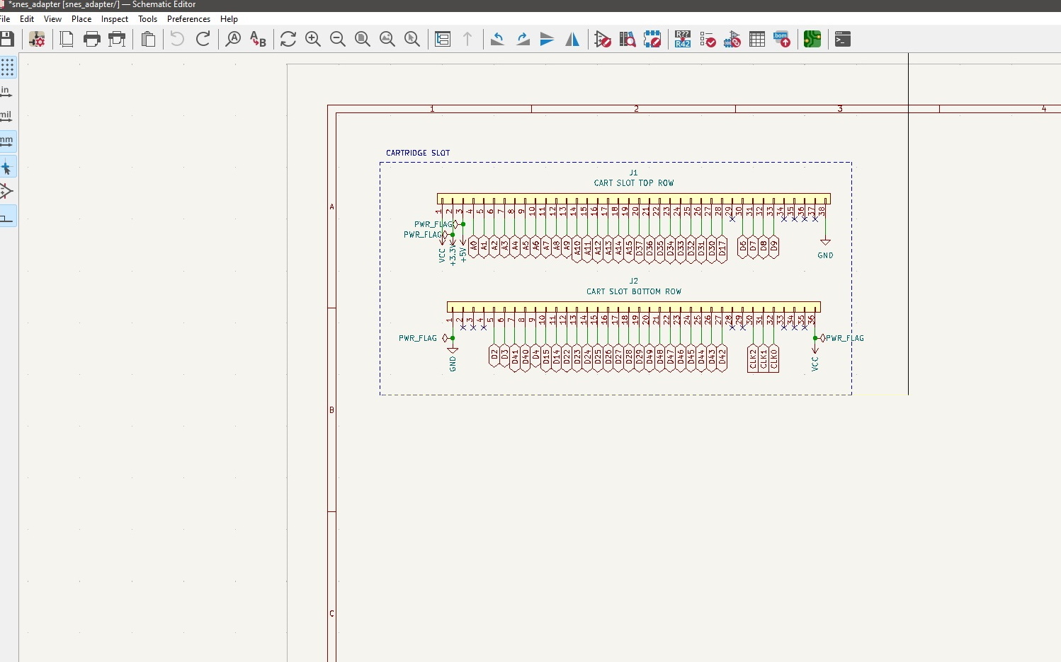
Open the kicad_sch file
Delete everything you don't need
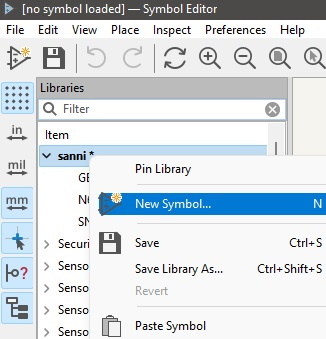
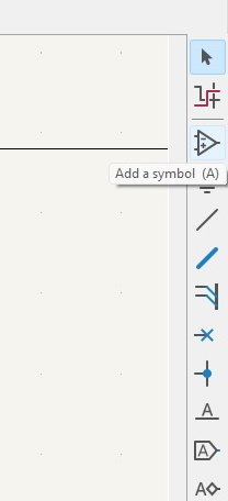
Open the symbol editor
Right-click on the OSCR library and select new symbol
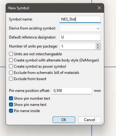
Give the new symbol a name
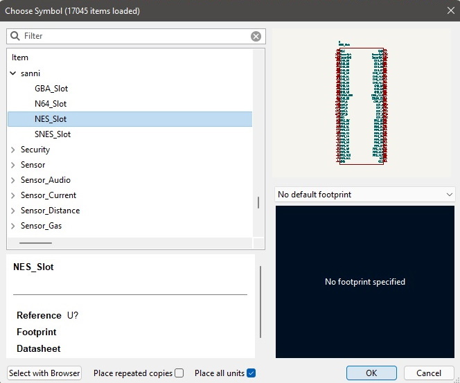
If you want you can copy&paste from another symbol
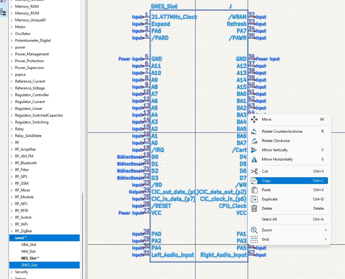
Then you can rearrange everything until it matches the desired pinout and save
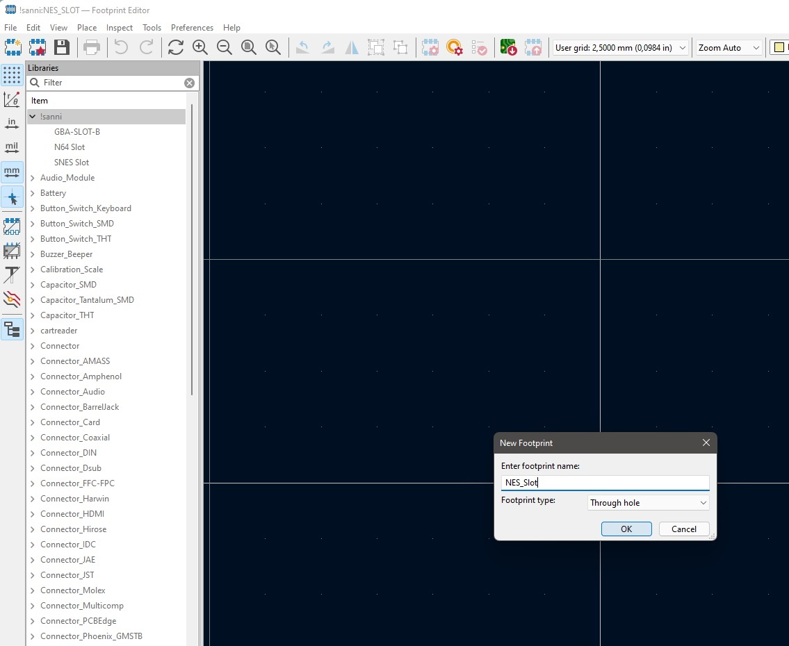
Open the footprint editor
Locate the OSCR library and create a new through-hole footprint
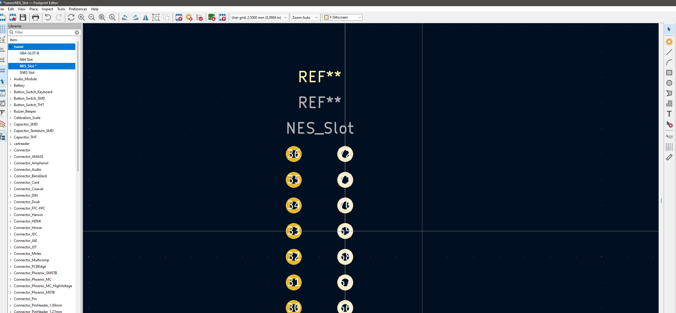
Now place the needed pads, make sure you don't mix up the pin numbers compared to your symbol. You can choose a grid with the same spacing as the pin spacing of your cartridge slot to place the pads more quickly. Save once finished.
Back in the schematics editor you can now place the newly created symbol
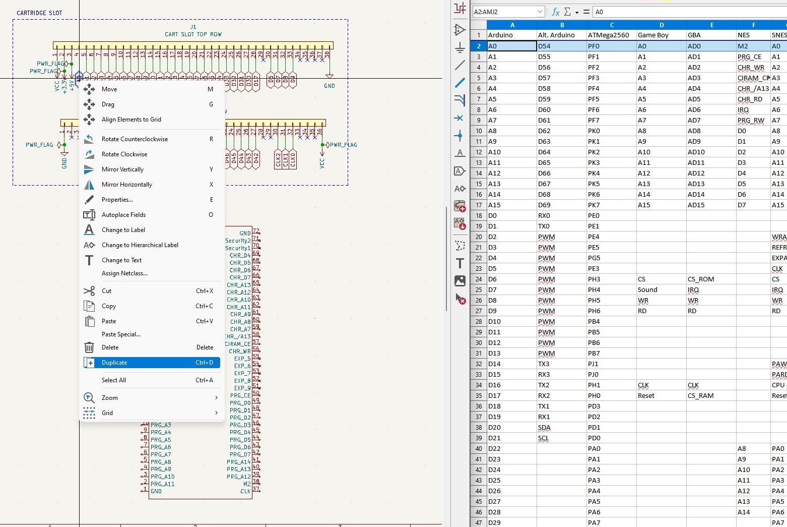
Open your pinout next to the schematics editor. Now duplicate(Ctrl+D) the little flags next to the Cart Slot Top/Bottom Row pins one by one and move(m) and rotate(r) them to the right position on your newly added symbol.
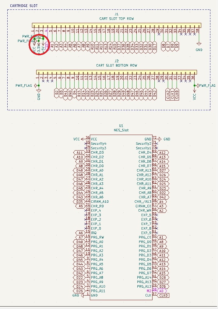
Once done you also need to connect either the +5V or +3.3V pin to the VCC pin according to the voltage your cartridge needs using the line tool to make the adapter compatible with HW4, HW5 ignores this and has its own voltage switch. Also make sure you give your symbol a reference name like U1.
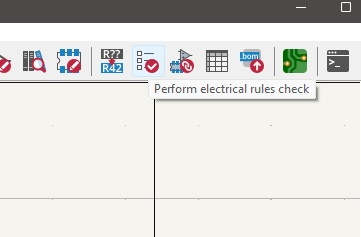
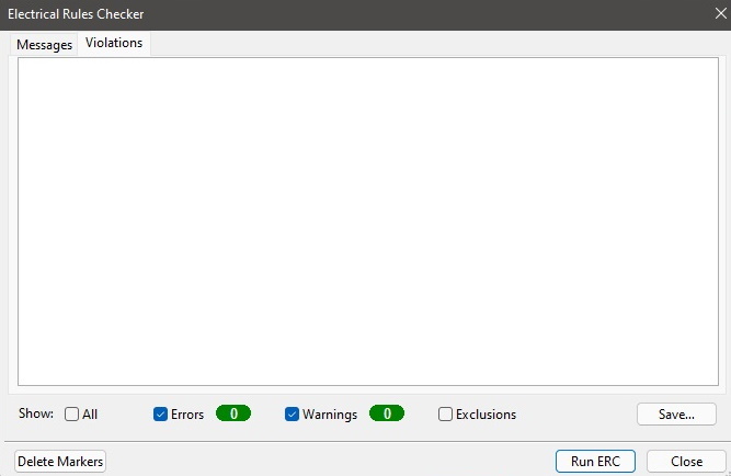
Now perform an electrical rules check and fix all error that appear and save
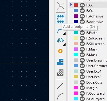
Open the kicad_pcb file again and add your newly created footprint
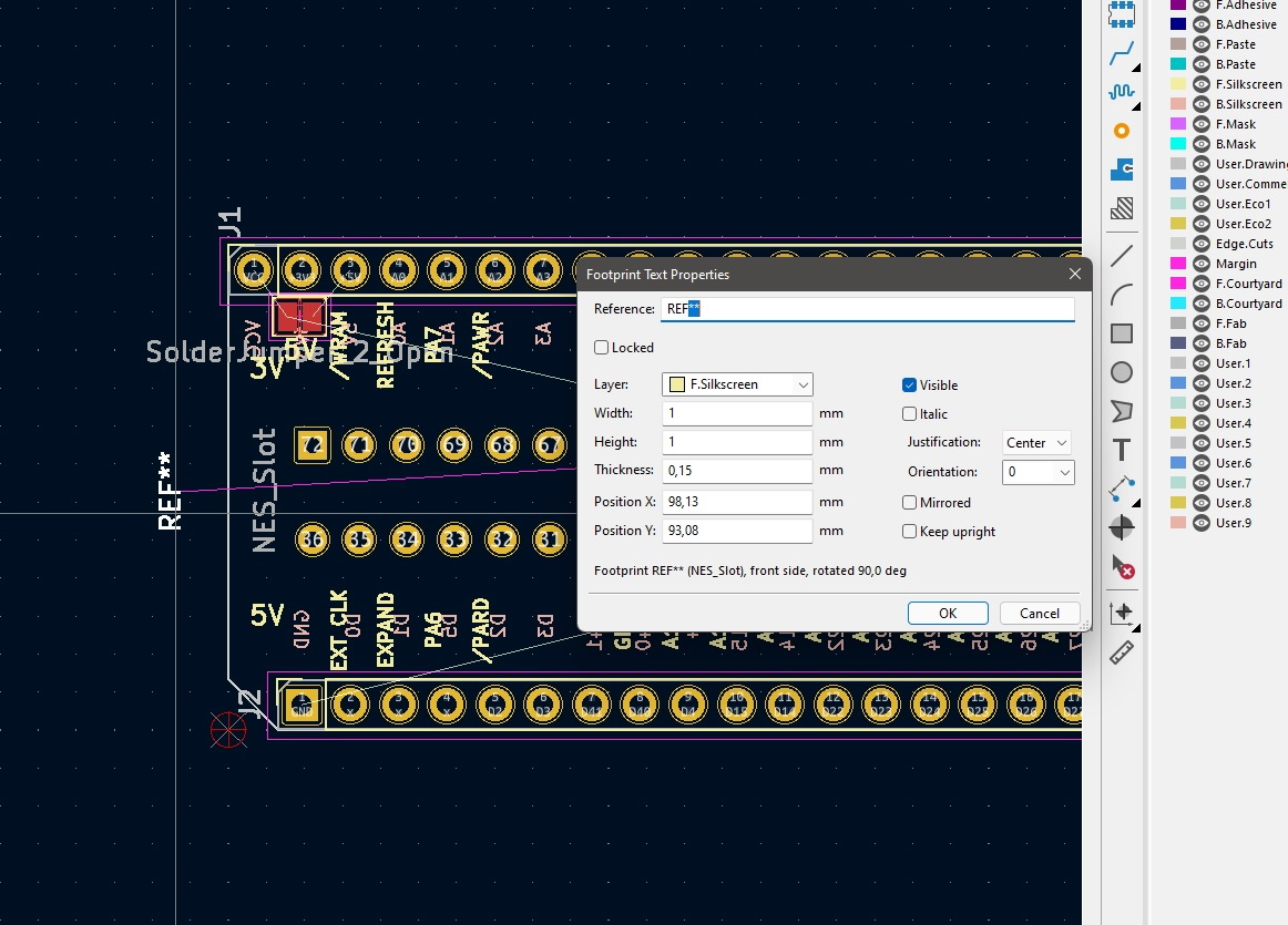
Give it the same name as you have given the symbol in the schematic
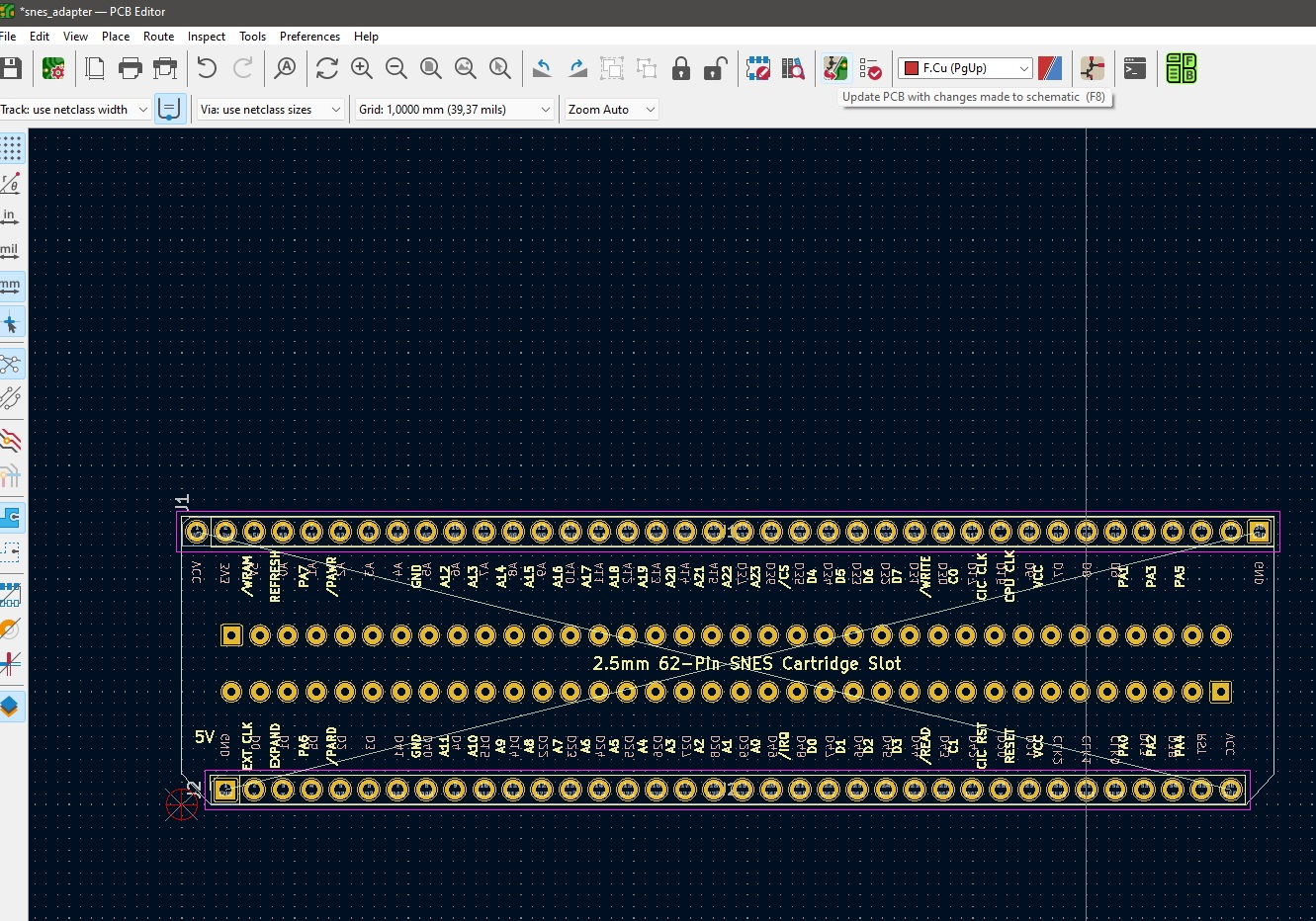
Press the "Update PCB with changes made to schematic" button
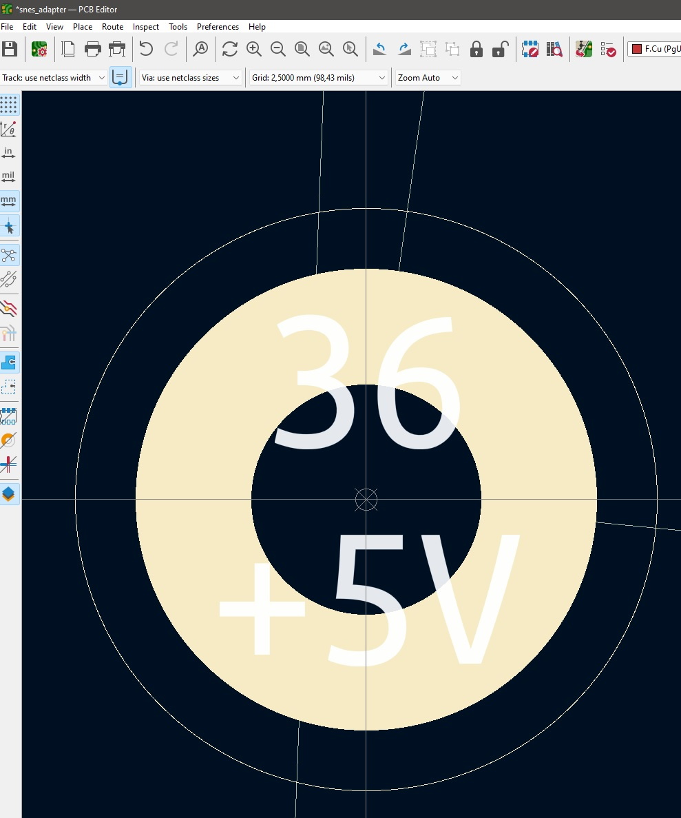
For the next step it is best if you align the grid to your solder pads. So choose same grid spacing as your pin spacing of your cartridge slot, then select a pad of your cartridge slot and press (m) then press (s) and left click. There should now be a little crosshair in the center of the pad and the grid should be aligned to the cartridge slot.
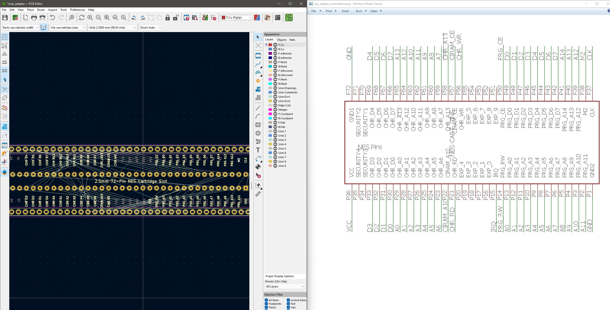
In the F.Silkscreen layer use the text tool to write the pinout next to each pin. This makes trouble shooting later easier. Once done save.
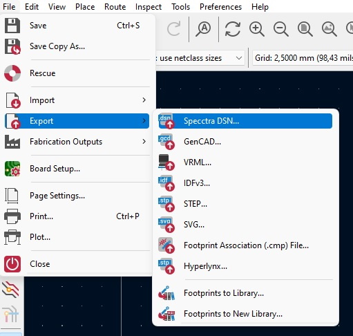
Now select "Export" and "Specctra DSN"
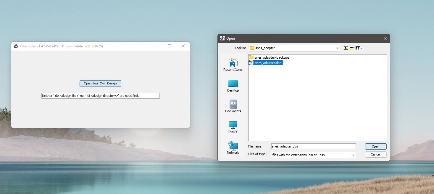
Launch FreeRouting and open the dsn file that you just exported
Click "Autorouter" and wait a little
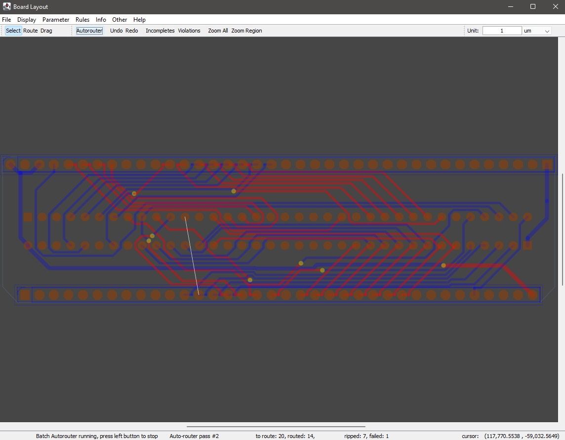
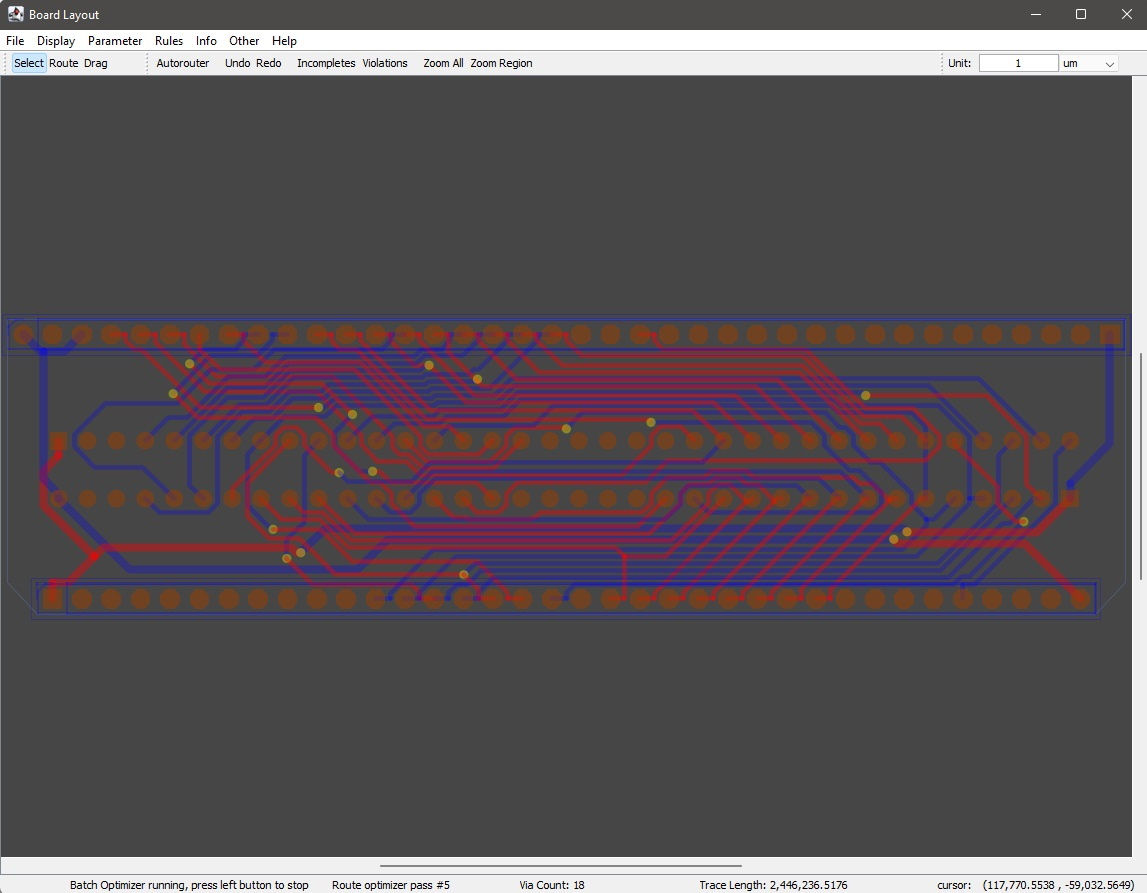
Once the routing is done the batch optimization will start which can take quite some time
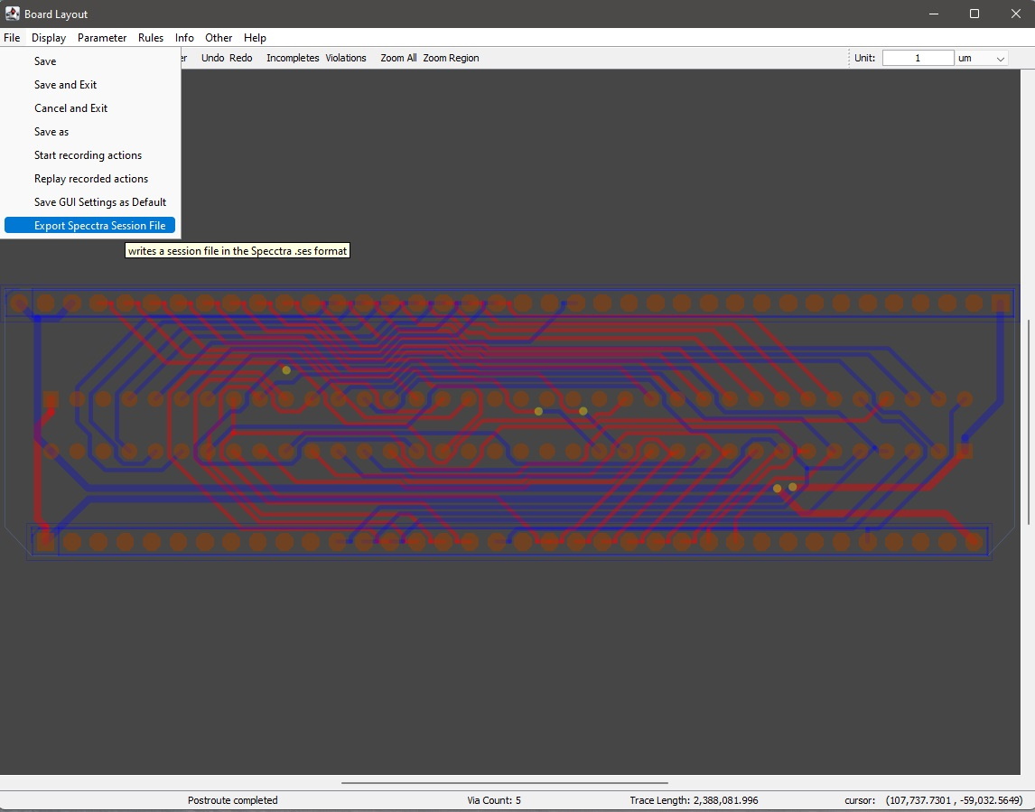
As soon as it has finished you can select "Export Specctra Session File"
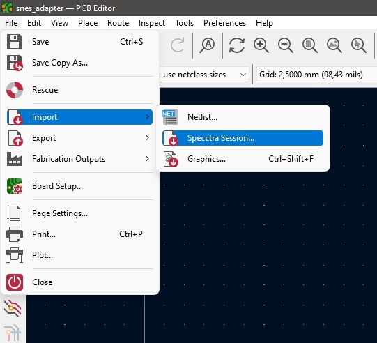
Import the session file in KiCad
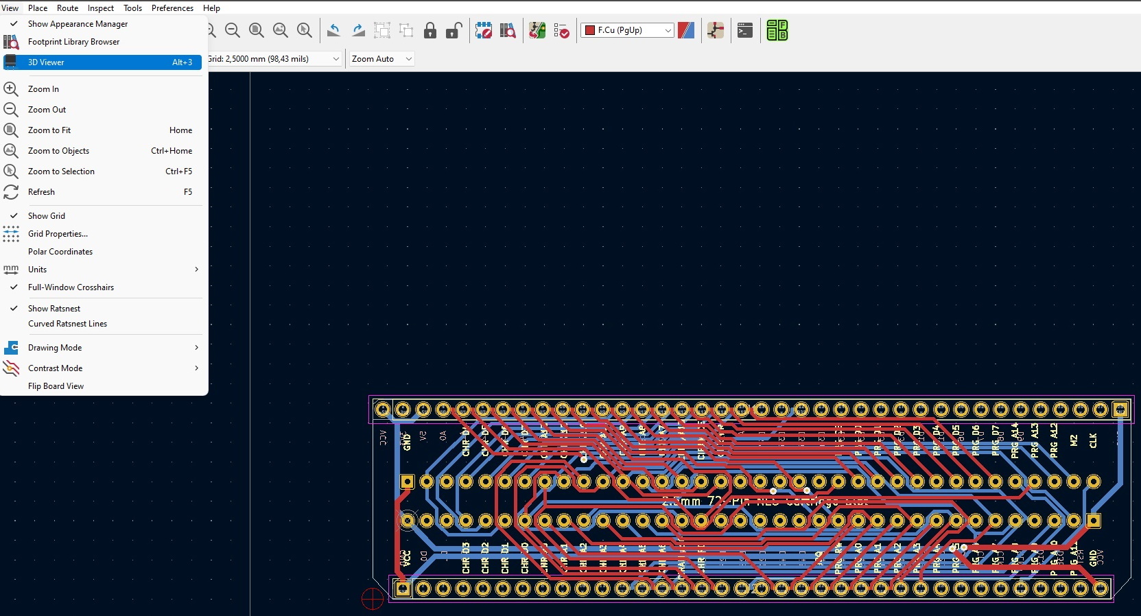
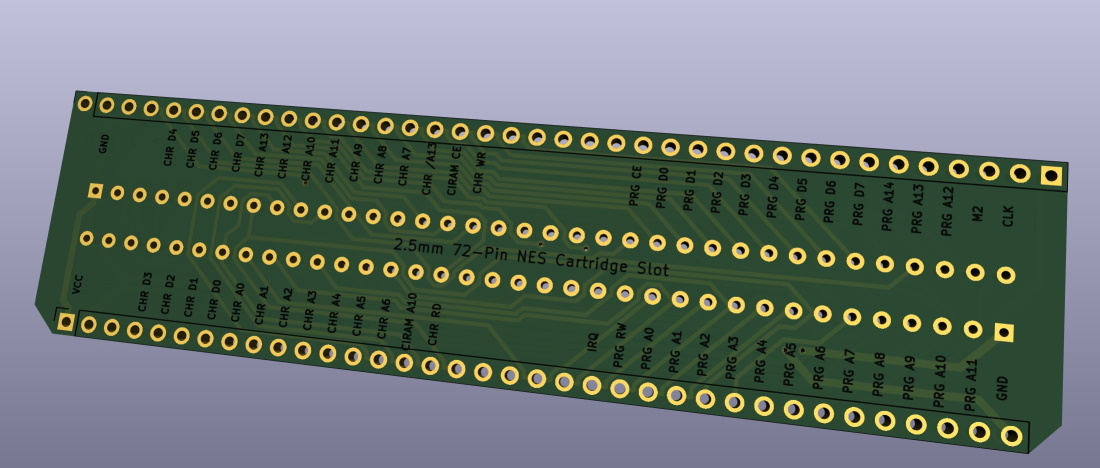
Press "Show the design rules checker window" to fix any issues. This step is super important, especially after using the autorouter. After that open the 3D viewer to check if the silkscreen looks ok too
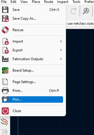
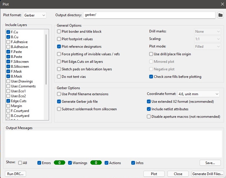
Finally select "Plot"
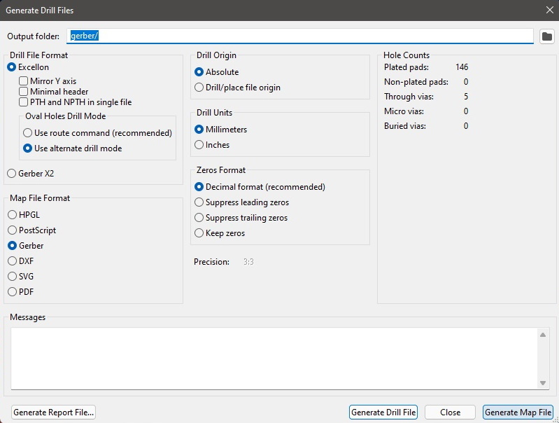
Press the "Plot" button and the "Generate Drill Files" button
Press the "Generate Drill File" and "Generate Map File" buttons
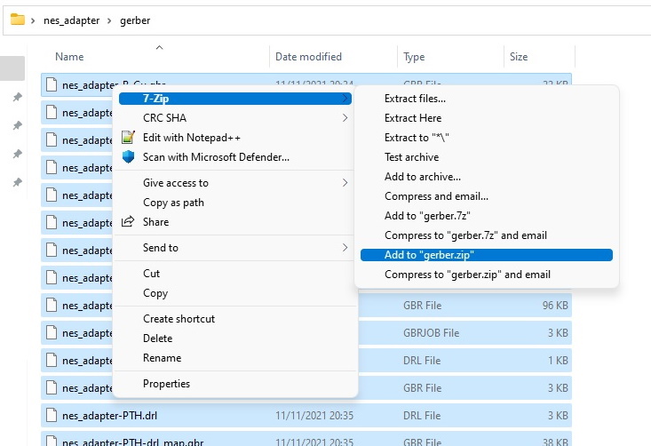
Finally put all the Gerber files into a zip and upload it to a PCB maker