Kickstart Switcher v1 - keirf/pcb-projects GitHub Wiki
If you have received this switcher in kit form then please read these instructions from start to finish. If you have received this switcher fully assembled then you can skip to the last section ("Installing the ROM").
A ROM is an array of storage locations indexed by a binary-encoded address at the address pins of the chip. The standard 512kB Amiga ROM is 256k x 16-bit words, addressed by pins A0-A17. Larger ROMs require an extra address pin for each doubling of capacity: A18 (1MB), A19 (2MB), and so on.
These larger ROMs can be considered a banked (or multi-ROM-image) version of the 512kB ROM: A0-A17 address the currently selected 512kB bank (aka ROM image), while A18+ select between 2 or more banks.
The purpose of the Kickstart switcher, then, is to control the bank-selection pin(s). Since this design switches between 2 ROM images, it controls just one address pin (A18) via its output (called 'Sel'). A0-A17 remain under control of the Amiga hardware. A19+, if present, can be tied to a fixed value.
The switcher defaults to Sel=0 at startup. The output is toggled by seeing a low pulse at its input (called 'Rst') which is longer than around 4 seconds. The input is expected to be attached to the active-low reset line of the Amiga, so that holding Ctrl-Amiga-Amiga for multiple seconds will trigger the Kickstart switch.
For each self-build kit, the following parts are supplied (package type in brackets where applicable):
- 1 x PCB
- 1 x 74HC14 (SOIC-14)
- 1 x 74HC74 (SOIC-14)
- 4 x 1K resistor (0805) [marked '1001']
- 3 x 1M resistor (0805) [marked '1004']
- 3 x 0.1uF MLCC (0805) [thin brown chip]
- 1 x 22uF MLCC (0805) [thick brown chip]
- 1 x 4.7uF tantalum (2012) [yellow with anode marking]
- 1 x N MOSFET (SOT23)
- 1 x right-angled pcb header pin
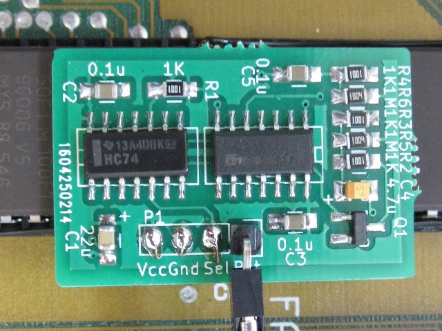
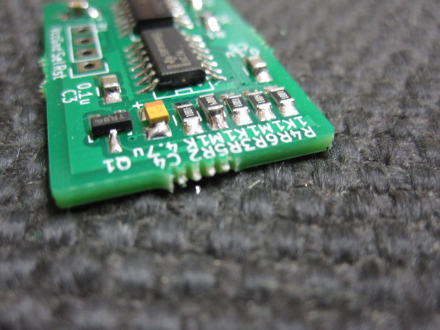
See the closeup picture for a build guide. Take care with the orientation of parts: the SOICs have a bevelled edge on the side with pin 1; the tantalum capacitor has a bar marking the anode (+).
In location R5 the 1M resistor gives a reset-to-switch delay of 4 seconds. A second 1M resistor is provided which can be stacked on the first to halve the delay to 2 seconds.
Soldering advice:
-
Use flux (flux pens can be picked up cheaply from China on Ebay). Flux pads before applying solder to help it flow and avoid blobby joints. This is particularly useful for fine solder.
-
Use fine solder, around 0.4mm works well. If your solder is too thick it is easy to over-apply and end up with blobby joints.
-
Use a regulated soldering station, set it to about 350C, and use a conical tip (but not too fine) or a small chisel tip (say up to 2mm). The tip wants to be big enough to get heat to the part but not too cumbersome for the detailed work. If using a conical tip apply it at an angle to increase surface area.
-
The 0805 passive components tend to move around while soldering. To avoid this, apply solder to one pad. Now hold the component in place with tweezers and re-heat the pad. This will tack the component in place. Now solder the second pad as usual, and return to the first pad and add extra solder as required.
-
If you end up with a messy joint, apply more flux and re-heat. The solder should reflow and make a nicer joint. If there is still to much solder, remove some with solder wick.
-
Use flux. :)
This step requires a blank 27C800 or 27C160. Also typically you will use a TL866 programmer and the 27C160 adapter which I build and sell. You require 512kB ROM images which are 'byte-swapped' (bytes in each 16-bit word are swapped). If this is done correctly then, when loaded into the MiniPro programming software, the Kickstart copyright message will appear in the buffer window ungarbled. If it's garbled, you haven't swapped! If you are using a 256kB image (eg Kickstart 1.3) then double it up.
In Linux or MacOS terminals, the double-up and byte swap could be done as follows:
 # dd if=kick13.rom of=kick13_swapped.rom conv=swab
 # cat kick13_swapped.rom >kick13_swapped_doubled.rom
 # cat kick13_swapped.rom >>kick13_swapped_doubled.rom
On Windows you will have to find your own way!
Plug my adapter into the TL866 and set the jumpers to
A19/A18=0/0. Select device 27C4096, deselect Check ID and set
VPP Voltage 12.50V (optional, but seems to work and closer to 27C160
specs). Insert the EPROM into the adapter. Load your default ROM image
and program the EPROM.
Now load your second ROM image, select A19/A18=0/1, and program
the EPROM.
The 27C800/27C160 must be physically modified to support the Kickstart switcher. In the below steps you can ignore pin 42 on 27C800, or even cut it off entirely, as it's unused.
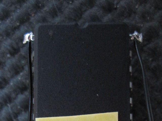
-
Cut pins 1 (A18) and 42 (A19) short, but with enough left to solder onto.
-
Flux pins 1, 22, 31, 42.
-
Apply solder to all fluxed pins and then attach a short piece of hookup wire ('Kynar' wire, or a strand from an ATA 80 ribbon cable is appropriate here) to each one.
-
Attach the switcher to the top of the EPROM with glue or double-sided tape with header P1 on the right-hand side. Pre-programmed EPROMs are supplied with tape already installed.
-
Connect pin 22 (VCC) to P1:Vcc on the switcher.
-
Connect pin 31 (VSS) and pin 42 (A19) to P1:Gnd on the switcher.
-
Connect pin 1 (A18) to P1:Sel on the switcher.
The ROM is directly compatible with any single-ROM Amiga with a 42-pin ROM socket. In this case insert the ROM with its pin 1 in pin 1 of the socket (however since this pin is cut short, it will of course not make contact with the socket).
If the Amiga has a 40-pin socket then ensure that pin 31 of the socket is connected to VCC. This is true for A500 Rev 6 and later, A500 Plus, and A600, among others. If compatible, insert the ROM with pin 2 in pin 1 of the socket (ie. the shortened pins overhang the socket).
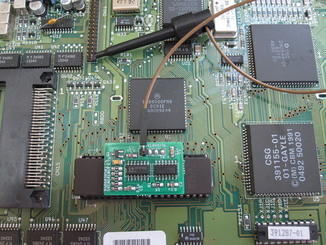
Now you must attach P1:Rst of the switcher to the Amiga's reset line. A jumper wire and probe clip are supplied for this purpose (separately if supplied in kit form; soldered together in assembled form).
WARNING: The ROM will not work reliably until connected to the reset line. It will switch randomly between the programmed Kickstart images causing crashes.
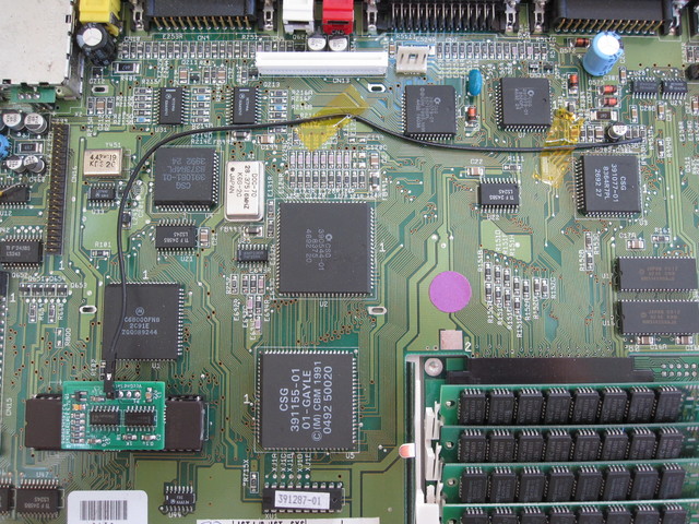
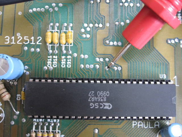
Clip to the leg of any DIL chip connected to the _RST line. Paula pin 11 is a good choice (see picture). You may need to bend and/or open up the probe clip a little to hook it around the chip pin -- make sure to retract the clip as far as possible and snug the probe up against the pin, and check that the clip does not touch any adjacent pin.
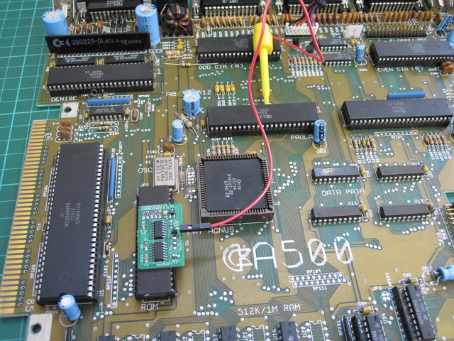
If you want a more permanent connection, _RST is available at various vias on the A500 motherboard (eg. there is one near Paula on at least Rev 6A: see below) or at resistor array RP101. A buzz test with a multimeter for continuity with Paula pin 11 will confirm that a via or track carries _RST.
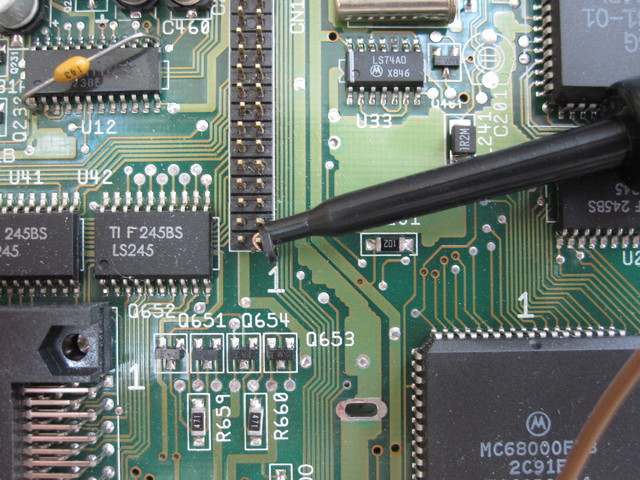
Similar to A500 you can clip to any DIL chip connected to the _RST line: eg. Paula pin 11, 68000 pin 18, or Gary pin 41.
Clip to pin 1 of the IDE port if it is unused.
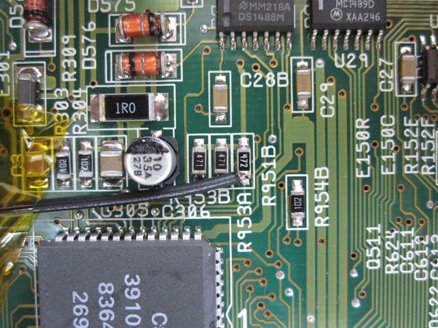
Otherwise you will need to solder to resistor R951B near Paula.