Shifting Register 74HC595 IC - jlopez6077/STM32_Components_Library GitHub Wiki
Understanding the 74HC595 IC

It's an 8-bit register with a total of 16 pins.
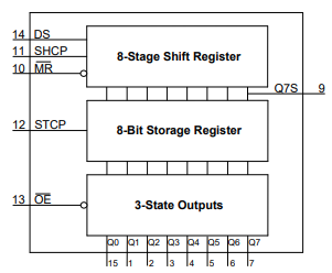
Data is first transmitted using the DS (Serial Data Input) pin. Serial meaning one bit at a time. With each cycle of the SHCP (Shift Register Clock Input), the value of the DS gets shifted one bit, inside the 8-Stage Shift Register. Both DS and SHCP are controlled by SPI (Serial Peripheral Interface) in your microcontroller. SPI is a synchronous communication protocol, meaning both the transmitter and receiver share the same clock signal.
MR (Master Reset Input) pin is low active. Meaning that to clear the Shift Register, the pin needs to be low.
The Q7S (Serial Data Output) pin is used if you want to connect another shifting register. In this example, we won't be using the Q7S pin. The opinion is there if you need a larger register.
Assuming SPI has transmitted the data to the 8-Stage Shift Register, it's time to cycle the STCP (Storage Register Clock Input) pin. The data from the Shift Register is loaded into the Storage Register. It's parallel loaded so all 8 bits are transferred at once.
Lastly, the OE (Output Enable Input) Pin is activated. It's low active and it allows the data to be outputted through Q0-Q7. The OE pin isn't essential so for our setup it's grounded. This way it's always outputting the data.
Configuring your Pins
In your Pinout & Configuration tab, you'll need to go to the Connectivity section. There you will find SPI1. The mode will be Transmit Only Master. Under Parameter Settings, change Data Size to 8 bits. Also, note that First Bit is MSB First. What this means is that the most significant bit is going to be Q7 on the register.

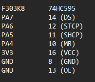
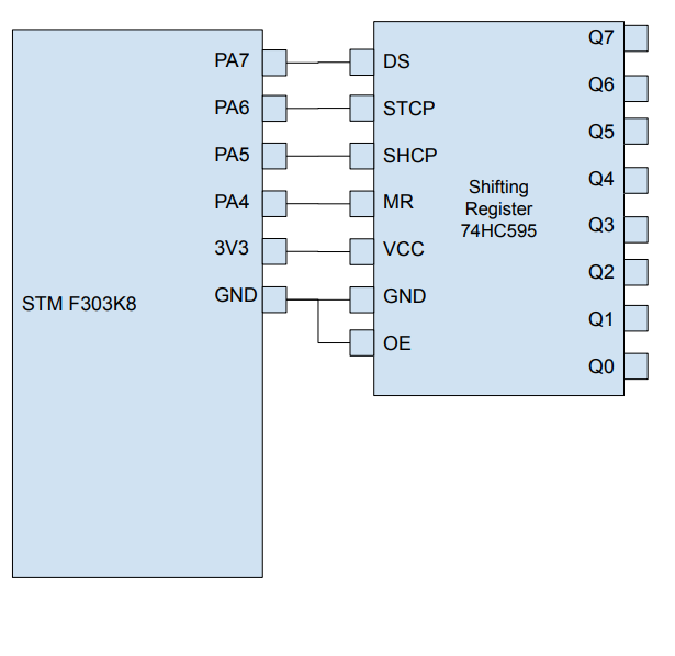
This will automatically assign Pin PA5 as SPI1_SCK. That is the SHCP pin. Also, PA7 was assigned as SPI1_MOSI. That is the DS pin.
Next, assign PA6 and PA4 as GPIO_Output. These will be your STCP and MR pins.
After that, generate your code.
Pin Connection

Code
The file is called register.h and can be found in the components folder.
define section
// 74HC595 IC REGISTER PINS
#define STORAGE_REGISTER_CLOCK_PIN GPIO_PIN_6	// PA6
#define MASTER_CLEAR_PIN GPIO_PIN_4		// PA4
#define REGISTER_PORT GPIOA			// GPIOA

#define BYTE_SIZE 1				// Data Size
If you used different pins for your GPIO_Outputs then here is were you can change those. For example, lets say I didn't want PA6 as my SHCP pin. I want to use PA11 instead. I would write this:
#define STORAGE_REGISTER_CLOCK_PIN GPIO_PIN_11 // PA11
Just note that both PA11 and PA6 have the same register port. They are both GPIOA. If you wanted to use GPIOB instead then you would have to change the function manually.
function
void sendSPIdata(SPI_HandleTypeDef hspi1, uint8_t data[])
/*
 * @param  hspi to a SPI_HandleTypeDef structure that contains
 *               the configuration information for SPI module.
 * @param  Data address to data buffer
 */
{
	// clear the shift register buffer
	HAL_GPIO_WritePin(REGISTER_PORT, MASTER_CLEAR_PIN, GPIO_PIN_RESET);	// Low Active

	// open shift register buffer
	HAL_GPIO_WritePin(REGISTER_PORT, MASTER_CLEAR_PIN, GPIO_PIN_SET);

	// transmit data
	HAL_SPI_Transmit(&hspi1, &data[0], BYTE_SIZE, 10); 			//controls SPI1_MOSI and SPI1_SCLK

	// parallel load into storage register
	HAL_GPIO_WritePin(REGISTER_PORT, STORAGE_REGISTER_CLOCK_PIN, GPIO_PIN_SET);
	HAL_GPIO_WritePin(REGISTER_PORT, STORAGE_REGISTER_CLOCK_PIN, GPIO_PIN_RESET);
}
First you'll find a comment explaining what parameters it takes. Then it's the function itself.
How to Use
- Copy register.h file into your project.
- Include it into your main.c file.
/* Private includes ----------------------------------------------------------*/
/* USER CODE BEGIN Includes */

#include "register.h"
/* USER CODE END Includes */
- Create an array of 8-bits
  /* USER CODE BEGIN 2 */
  uint8_t SPIdata[] ={0xff}; // 0xff is how you write ff in hexadecimal
  /* USER CODE END 2 */
- Call the function
/* Infinite loop */
  /* USER CODE BEGIN WHILE */
  while (1)
  {
    /* USER CODE END WHILE */
	  sendSPIdata(hspi1, &SPIdata[0]);  // hspi1 is initialized when code is generated, 1111 1111 is sent to register
	  HAL_Delay(500);                   // 500 ms delay
    /* USER CODE BEGIN 3 */
  }
  /* USER CODE END 3 */
}