FPGA Communication - hampussandberg/HexConnect GitHub Wiki
To simplify the controller on the FPGA the command format below is used. This gives the FPGA the time it takes to transmit one byte to process the command and data.

Command format with returning data
This means that sending a command that does not return anything will result in two bytes sent, while a command that will return data requires four bytes minimum to be sent.
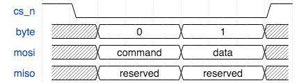
Command format without returning data
0x00 - Status
Description: Status of the data processor
Return byte:
| Bit7 | Bit6 | Bit5 | Bit4 | Bit3 | Bit2 | Bit1 | Bit0 |
|---|---|---|---|---|---|---|---|
| res | res | res | res | res | res | res | Ready |
Ready: Set to 1 when the data processor is ready, otherwise 0
0x10 - Channel Power
Compatible modules: All
Description: Controls the input of the TPS22960 load switch connected to each module
Data byte:
| Bit7 | Bit6 | Bit5 | Bit4 | Bit3 | Bit2 | Bit1 | Bit0 |
|---|---|---|---|---|---|---|---|
| Op[1] | Op[0] | Ch6 | Ch5 | Ch4 | Ch3 | Ch2 | Ch1 |
Operation (Op[1:0]):
- Op=0x0: Get Current Power
- Op=0x1: Enable Power
- Op=0x2: Disable Power
- Op=0x3: reserved
Channel (Ch6 - Ch1): When a bit is set the operation will be performed for that channel
Return byte:
| Bit7 | Bit6 | Bit5 | Bit4 | Bit3 | Bit2 | Bit1 | Bit0 |
|---|---|---|---|---|---|---|---|
| 0 | 0 | Ch6 | Ch5 | Ch4 | Ch3 | Ch2 | Ch1 |
0x11 - Channel Output
Compatible modules: GPIO Module, CAN Module, RS-232 Module
Description: Manages the output switch for the modules that has a relay on the outputs
Data byte:
| Bit7 | Bit6 | Bit5 | Bit4 | Bit3 | Bit2 | Bit1 | Bit0 |
|---|---|---|---|---|---|---|---|
| Op[1] | Op[0] | Ch6 | Ch5 | Ch4 | Ch3 | Ch2 | Ch1 |
Operation (Op[1:0]):
- Op=0x0: Get current output
- Op=0x1: Enable output
- Op=0x2: Disable output
- Op=0x3: reserved
Channel (Ch6 - Ch1): When a bit is set the operation will be performed for that channel
Return byte:
| Bit7 | Bit6 | Bit5 | Bit4 | Bit3 | Bit2 | Bit1 | Bit0 |
|---|---|---|---|---|---|---|---|
| 0 | 0 | Ch6 | Ch5 | Ch4 | Ch3 | Ch2 | Ch1 |
0x12 - Channel ID
Compatible modules: All
Description: Manages the channel ID of the modules
Data byte:
| Bit7 | Bit6 | Bit5 | Bit4 | Bit3 | Bit2 | Bit1 | Bit0 |
|---|---|---|---|---|---|---|---|
| Op[1] | Op[0] | Ch6 | Ch5 | Ch4 | Ch3 | Ch2 | Ch1 |
Operation (Op[1:0]):
- Op=0x0: Get channel ID
- Op=0x1: Update channel ID
- Op=0x2: Stop updating channel ID
- Op=0x3: reserved
Channel (Ch6 - Ch1): When a bit is set the operation will be performed for that channel
Return byte(s):
| Bit7 | Bit6 | Bit5 | Bit4 | Bit3 | Bit2 | Bit1 | Bit0 |
|---|---|---|---|---|---|---|---|
| 0 | 0 | 0 | ID[4] | ID[3] | ID[2] | ID[1] | ID[0] |
Channel ID (ID[4:0]): The ID for the requested channel. If more than one channel was specified they will be returned in different bytes with the lowest numbered channel first.
0x13 - Channel Direction
Compatible modules: GPIO Module, RS-232 Module
Description: Manages the direction of the data to and from the module
Data byte:
| Bit7 | Bit6 | Bit5 | Bit4 | Bit3 | Bit2 | Bit1 | Bit0 |
|---|---|---|---|---|---|---|---|
| res | res | Op[1] | Op[0] | SubCh | Ch[2] | Ch[1] | Ch[0] |
Operation (Op[1:0]):
- Op=0x0: Get channel direction
- Op=0x1: Set channel direction
- Op=0x2: reserved
- Op=0x3: reserved
Subchannel (SubCh):
- SubCh=0x0: Subchannel A
- SubCh=0x1: Subchannel B
Channel (Ch[2:0]):
- Ch=0x0: reserved
- Ch=0x1-0x6: Channel no 1 to 6
- Ch=0x7: All channels
0x30 - Termination
Description: Manages the switching of the termination resistor between CAN_HIGH and CAN_LOW
Data byte:
| Bit7 | Bit6 | Bit5 | Bit4 | Bit3 | Bit2 | Bit1 | Bit0 |
|---|---|---|---|---|---|---|---|
| Op[1] | Op[0] | Ch6 | Ch5 | Ch4 | Ch3 | Ch2 | Ch1 |
Operation (Op[1:0]):
- Op=0x0: Get current termination
- Op=0x1: Enable termination
- Op=0x2: Disable termination
- Op=0x3: reserved
Channel (Ch6 - Ch1): When a bit is set the operation will be performed for that channel
Return byte:
| Bit7 | Bit6 | Bit5 | Bit4 | Bit3 | Bit2 | Bit1 | Bit0 |
|---|---|---|---|---|---|---|---|
| 0 | 0 | Ch6 | Ch5 | Ch4 | Ch3 | Ch2 | Ch1 |