Upconverter_Design_Details - ha7ilm/opendous GitHub Wiki
Upconverter
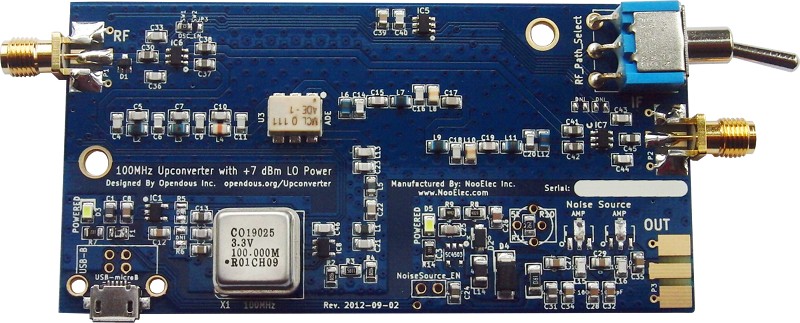
Design
The Upconverter is a passive Double-Balanced Mixer with RF switches at input and output to allow a Passthrough mode. Power is sourced from a standard USB-microB connector to allow powering via mobile device chargers. The switch controls the signal path, Passthrough or Upconvert, and mirrors the board layout. Switch towards the SMA connector is Upconvert, towards PCB edge for Passthrough.
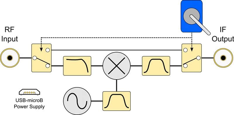
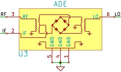
RF and IF ports in a Double-Balanced Mixer are interchangeable but there is more LO-to-RF Isolation than LO-to-IF Isolation. To reduce LO radiation through the antenna, the RF port is used as input.
The mixer used is the Mini-Circuits ADE-1 with a low LO Power Level to reduce noise and better receive weak signals. The LO Level is nominally +7dBm which puts the 1dB compression point at +1dBm (this is the maximum input signal level before distortion occurs). Upconversion losses are around 10dB.
RF Input Low-pass Filter
The input Low-pass filter is an Elliptic (Cauer) filter used for its sharp transition between passband and stopband. This ensures higher input frequencies do not mix with the intended output products.

The filter was designed to have less than 1dB of ripple in its passband and a 3dB cutoff at the lower input range of cheap DVB dongles being repurposed for SDR.

The input switch and filter together manage to keep passband ripple below 1.5dB. This data plot was created using a VNWA freshly calibrated for 0.1MHz to 120MHz.

LO Band-pass Filter
Most oscillators show significant bleed of the internal frequency used in their multiplier circuitry. With 100MHz oscillators the internal frequency tends to be in the 20-25MHz range, directly in the HF band of interest. To reduce these frequencies at the output and also help reduce LO harmonics, a Bessel band-pass filter is used for its minimal phase distortion to keep the LO signal as clean as possible.

The attenuator and filter are used to reduce the LO level to an optimal value.

125MHz LO Band-pass Filter
The 6dB attenuator and filter are needed to reduce the LO level to the +7dBm optimal value and filter any oscillator spurious signals and harmonics.

The testing results:

LO Level
The following data plot was created using a VNWA freshly calibrated for 40MHz to 160MHz. Theory and practice clearly deviate here but the losses are acceptable for the LO signal. With the LO buffer running at 3.3V and outputting nearly a square wave (Vpk=Vrms), the LO level at the buffer is about 3.3Vp-p=1.6Vpk=1.6Vrms=17dBm. The LO level at the mixer is therefore approximately +7dBm.

IF Output Band-pass Filter
The output Band-pass filter is a Butterworth filter used for its lack of ripple in the passband. It is a 7th-order topology to ensure a sharp transition between passband and stopband. A band-pass filter was chosen to get the upconversion products of the mixer and to reduce LO harmonic products at the IF output.

The filter was designed to have a passpand between 100MHz and 150MHz (the upconverted 0.5MHz to 50MHz signals). Attenuation of LO harmonics/products and RF input frequencies is >30dB.

This data plot was created using a VNWA freshly calibrated for 70MHz to 200MHz. The filter and output switch manage to keep losses to about 3dB in the MF and HF Bands.

125MHz IF Output Band-pass Filter
The filter was designed to have a pass the Upconversion products and attenuate LO harmonics/products and RF input frequencies.

It has a 6dB bandwidth (data) of 121.5MHz to 193MHz and attenuates signals below 108MHz (FM Radio) by more than 26dB.

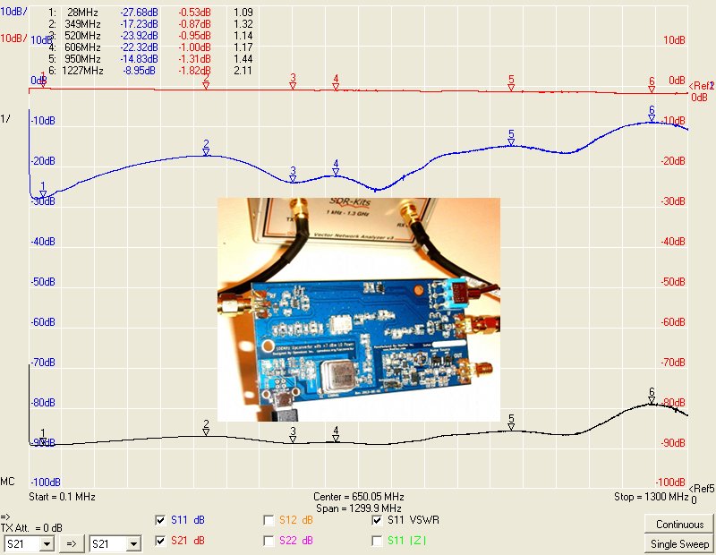
Passthrough Mode
This data plot was created using a VNWA freshly calibrated for 0.1MHz to 1300MHz. The AS169-73LF RF switches and PCB trace have losses of about 1dB up to around 1GHz.
Testing
There is a dedicated page for additional testing results.
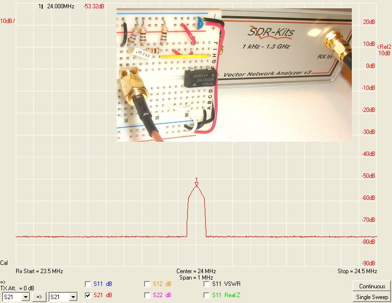
The following is the spectrum of a 24MHz oscillator (attenuated and DC-blocked). Note that the VNWA is not designed as a Spectrum Analyzer so the signal levels are not absolutely accurate but relative levels are useful.
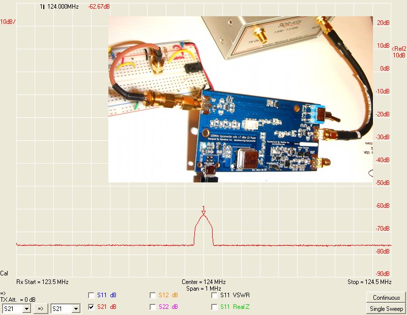
The following is the spectrum of the 24MHz oscillator upconverted to 124MHz. There is a ~9.35dB upconversion loss.
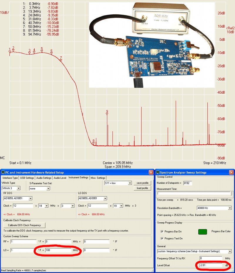
Conversion Losses
The following is the spectrum of the Upconverter with the tracking generator offset by 100MHz. This is a plot of the Upconversion losses which are below 10dB up to about 40Mhz, about 15dB at 50MHz, and hit the VNWA3 limits beyond 81MHz. The various peaks beyond are noise. The spectrum is vertically offset -2.61dB to make sure the 24MHz signal falls at 9.35dB loss, same as per the above Upconversion result for a 24MHz clock.
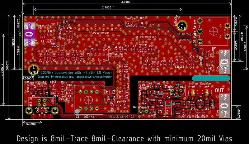
Layout
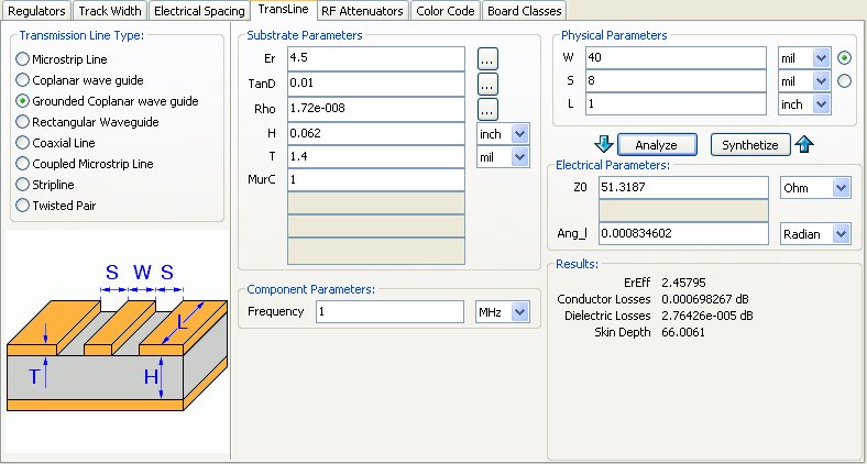
To reduce costs and allow for cheap prototyping, the board was designed to 2-layer 8-8-20 (8mil Trace, 8mil Clearance, and 20mil minimum drill size) specifications. A Coplanar Waveguide with Ground 40mil-Trace 8mil-Clearance structure provides the necessary 50-Ohm characteristic impedance over the intended frequency range. This happens to be about as wide as 0805 parts which allows for DIY'ability. The following image is of KiCad's PCB Calculator.
One side is a GND plane underneath all RF circuitry. Power is supplied through a PTC-protected USB-microB connector to allow powering the board using anything compatible with standard mobile device chargers. The 5V supply is converted to 3.3V with an RF LDO, the TPS79333. The 100MHz oscillator is buffered with a 74LVC1G126 gate to enable high drive levels and allow either TTL or CMOS output oscillators to be used. The oscillator is disabled when Passthrough mode is selected. Additional space that was leftover is used for a simple Noise Source.