KiCADTutorialCreatingGerberFiles - ha7ilm/opendous GitHub Wiki
This quick tutorial is for an older version of KiCad. The KiCad website has many newer tutorials.
This Tutorial uses the Micropendous1 project as an example.
After finishing your project you must set up KiCAD to produce well-defined Gerber files.
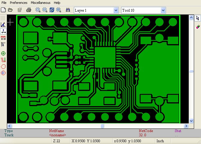
Open your PCB layout in PCBNew:
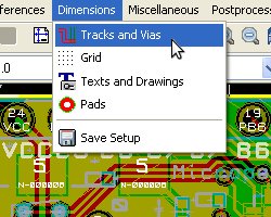
Select Tracks and Vias from the Dimensions Menu
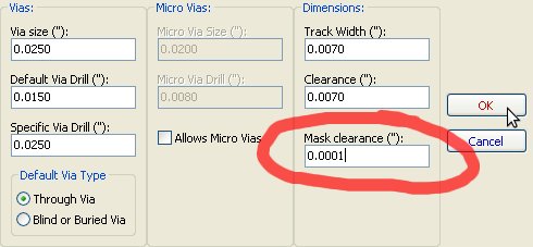
Now change the Mask Clearance from 0.0100 to 0.0001 and click OK.
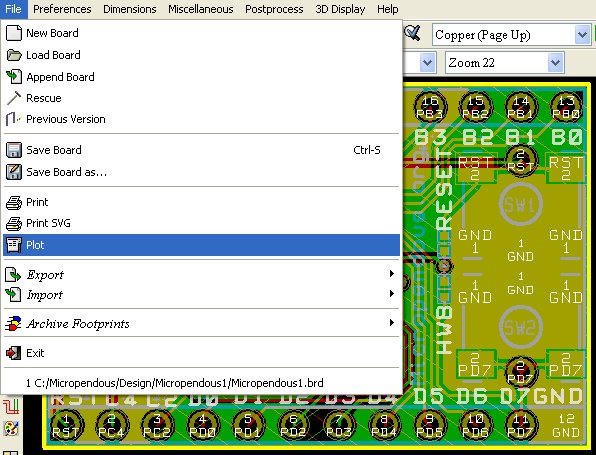
Now create the Gerber files. Select Plot from the File menu.
Select all the layers you want to plot. Here is an example list of the layers needed by one PCB manufacturer, GoldPhoenixPCB:
| KiCAD Layer Name | Gerber Name | Gerber Extension | GoldPhoenixPCB Extension |
|---|---|---|---|
| Copper | Bottom Layer | .GBL |
.BOT |
| Component | Top Layer | .GTL |
.TOP |
| SoldP_Cmp | Top Paste | .GTP |
.GBR |
| SilkS_Cmp | Top Overlay | .GTO |
.OVL |
| Mask_Cop | Bottom Solder Resist | .GBS |
.RES |
| Mask_Cmp | Top Solder Resist | .GTS |
.RES |
| Edges_Pcb | Edges | N/A | .GBR |
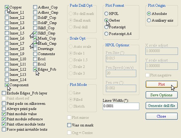
Click Plot to create the selected layers in the same directory as your project files. Note that KiCAD creates all Gerber files with the extension .pho. Depending on your PCB manufacturer, this may be acceptable or you may need to rename all files.
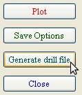
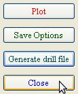
Now click the Generate Drill File button to create the drill file.
Your PCB fabricator may have specific requirements for these settings. The options selected in the picture below are somewhat standard.
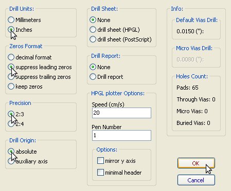
Click OK button to generate the drill file. Click Close in the Plot window to close. You are done creating Gerber files for PCB manufacturing.
Checking Gerber Files for Correctness
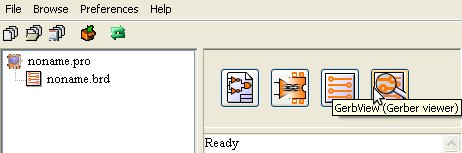
Start Gerber Viewer:
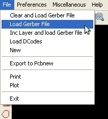
Select Load Gerber File from the File menu:
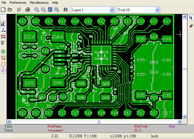
You can now use your mouse wheel to zoom in and out and examine your Gerber file.
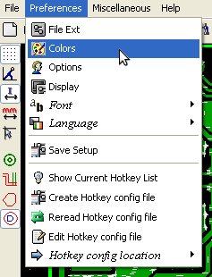
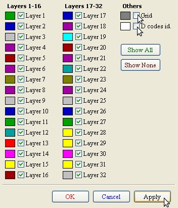
For easier examination, it helps to remove the white dcode markers. Select Colors from the Preferences menu:
Deselect Grid and D codes id. checkboxes and click OK.
Your Gerber files will now be more readable. Examine all of them carefully to make sure they describe your intended design.