ADC - glennlopez/EmbeddedSystems.Playground GitHub Wiki

ADC Initialization Registers
// Run Mode Clock Gating Control: base address 0x400F.E000
#define SYSCTL_RCGC2_R          (*((volatile unsigned long *)0x400FE108))
#define SYSCTL_RCGC0_R          (*((volatile unsigned long *)0x400FE100))

// GPIO PortE Registers: (APB) base address 0x4002.4000
#define GPIO_PORTE_DIR_R        (*((volatile unsigned long *)0x40024400))
#define GPIO_PORTE_AFSEL_R      (*((volatile unsigned long *)0x40024420))
#define GPIO_PORTE_DEN_R        (*((volatile unsigned long *)0x4002451C))
#define GPIO_PORTE_AMSEL_R      (*((volatile unsigned long *)0x40024528))

// ADC Registers: ADC0 base address 0x4003.8000	| ADC1 base address 0x4003.9000
#define ADC0_SSPRI_R            (*((volatile unsigned long *)0x40038020))
#define ADC0_ACTSS_R            (*((volatile unsigned long *)0x40038000))
#define ADC0_EMUX_R             (*((volatile unsigned long *)0x40038014))
#define ADC0_SSMUX3_R           (*((volatile unsigned long *)0x400380A0))
#define ADC0_SSCTL3_R           (*((volatile unsigned long *)0x400380A4))
#define ADC0_ACTSS_R            (*((volatile unsigned long *)0x40038000))
System Control Registers Base Address: 0x400F.E000
- System Control Legacy Registers (pg 234)
- RCGC0: 0x100 (pg 454)
- RCGC2: 0x108 (pg 462)
GPIO PORTE (APB) Base Address: 0x4002.4000
- Port Configuration Offsets (pg 657)
- GPIODIR: 0x400 - Direction (pg 660)
- GPIOAFSEL: 0x420 - Alternate Function Select (pg 668)
- GPIODEN: 0x51C - Digital Enable (pg 679)
- GPIOAMSEL: 0x528 - Analog Mode Select (pg 684)
Analog-to-Digital Converter (ADC) base address: ADC0 0x4003.800 & ADC1 0x4003.900
- Port Configuration Offsets (pg 657)
- SSPRI: 0x020 - ADC Sample Sequencer Priority (pg 838)
- ACTSS: 0x000 - ADC Active Sample Sequencer (pg 818)
- EMUX: 0x014 - ADC Event Multiplexer Select (pg 830)
- SSMUX3: 0x0A0 - ADC Sample Sequence Input Multiplexer Select 3 (pg 872)
- SSCTL3: 0x0A4 - ADC Sample Sequence Control 3 (pg 873)
ADC Initialization Routine
void ADC0_InitSWTriggerSeq3_Ch1(void){ volatile unsigned long delay;
  SYSCTL_RCGC2_R |= 0x00000010;   // 1) activate clock for Port E
  delay = SYSCTL_RCGC2_R;         //    allow time for clock to stabilize

  GPIO_PORTE_DIR_R &= ~0x04;      // 2) make PE2 input
  GPIO_PORTE_AFSEL_R |= 0x04;     // 3) enable alternate function on PE2
  GPIO_PORTE_DEN_R &= ~0x04;      // 4) disable digital I/O on PE2
  GPIO_PORTE_AMSEL_R |= 0x04;     // 5) enable analog function on PE2

  SYSCTL_RCGC0_R |= 0x00010000;   // 6) activate ADC0
  delay = SYSCTL_RCGC2_R;

  SYSCTL_RCGC0_R &= ~0x00000300;  // 7) configure for 125K
  ADC0_SSPRI_R = 0x0123;          // 8) Sequencer 3 is highest priority
  ADC0_ACTSS_R &= ~0x0008;        // 9) disable sample sequencer 3
  ADC0_EMUX_R &= ~0xF000;         // 10) seq3 is software trigger
  ADC0_SSMUX3_R = (ADC0_SSMUX3_R&0xFFFFFFF0)+1; // 11) channel Ain1 (PE2)
  ADC0_SSCTL3_R = 0x0006;         // 12) no TS0 D0, yes IE0 END0
  ADC0_ACTSS_R |= 0x0008;         // 13) enable sample sequencer 3
}
The code above will perform the following steps to configure the ADC for software start on one channel. The code shows specific details for sampling PE2, which is channel 1. The function ADC0_InSeq3 below will sample PE2 using software start and use busy-wait synchronization to wait for completion.
-
Step 1: We enable the port clock for the pin that we will be using for the ADC input.
- Set bit 4 in RCGC2 to enable the clock for PortE
SYSCTL_RCGC2_R |= 0x00000010;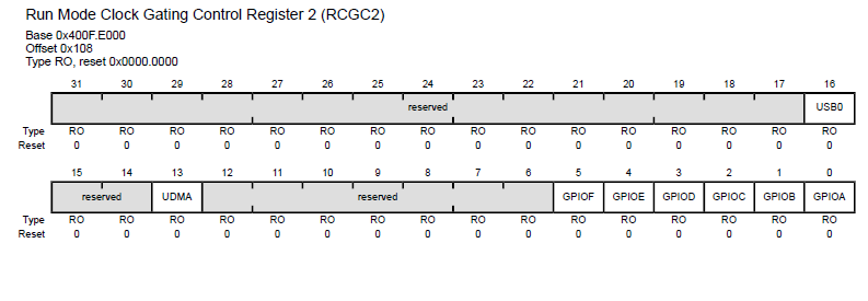
-
Step 2: Make that pin an input by writing zero to the DIR register.
- Clear bit 2 to make that port pin an input data direction
GPIO_PORTE_DIR_R &= ~0x04;
-
Step 3: Enable the alternative function on that pin by writing one to the AFSEL register.
- Set bit 2 to enable the alternative function
GPIO_PORTE_AFSEL_R |= 0x04;
-
Step 4: Disable the digital function on that pin by writing zero to the DEN register.
- Clear bit 2 to disable the digital function
GPIO_PORTE_DEN_R &= ~0x04;
-
Step 5: Enable the analog function on that pin by writing one to the AMSEL register.
- Set bit 2 to enable the analog function
GPIO_PORTE_AMSEL_R |= 0x04;
-
Step 6: We enable the ADC clock by setting bit 16 of the SYSCTL_RCGC0_R register.
- The RCGC0 register is used for controlling the ADC peripheral clock.
- Set bit 16 in RCGC0 register to enable the clock for ADC0
SYSCTL_RCGC0_R |= 0x00010000;
-
Step 7: Bits 8 and 9 of the SYSCTL_RCGC0_R register specify the maximum sampling rate of the ADC. In this example, we will sample slower than 125 kHz, so the maximum sampling rate is set at 125 kHz. This will require less power and produce a longer sampling time, creating a more accurate conversion.
- Clear bits 8 and 9 (MAXADC0SPD) in RCGC0 register to use 125K sample rate
SYSCTL_RCGC0_R &= ~0x00000300;

-
Step 8: We will set the priority of each of the four sequencers. In this example, we are using just one sequencer, so the priorities are irrelevant.
- The ADCSSPRI register is used for setting the priority for the sample sequencer.
- Make bits 13 and 12 in the SSPRI register 0 to set the to the highest priority
ADC0_SSPRI_R = 0x0123;-
Advantage of Sample Sequencer: Sequencers allow you to use the same ADC for multiple projects on same chip Each task/project has a sequencer and you assign channels to it.


-
Step 9: Before configuring the sample sequencer, we need to disable it. Disabling the sequencer during programming prevents erroneous execution if a trigger event were to occur during the configuration process.
- To disable sample sequencer 3, we write a 0 to bit 3 (ASEN3) in the ADC_ACTSS_R register.
ADC0_ACTSS_R &= ~0x0008;
-
Step 10: We configure the trigger event for the sample sequencer in the ADC_EMUX_R register.
- ADCEMUX register selects the event trigger that initiates the sampling for each sample sequencer (SS).
- For this example, we clear bits 15–12 (EM3) specifying software start mode for sequencer 3.
- Clearing bits 15-12 makes the trigger be initiated by setting the SSn bit in the ADCPSSI register (which we will use in ADC0_InSeq3 function below).
ADC0_EMUX_R &= ~0xF000;
-
Step 11: Configure the corresponding input source in the ADCSSMUXn register. In this example, we write the channel number to bits 3–0 in the ADC_SSMUX3_R register. In this example, we sample channel 1, which is PE2.
- There are 12 channels (0-11) to choose from. In this example we set SSMUX3 to 0x01 to use AIN1 (wired to PE2)
ADC0_SSMUX3_R = (ADC0_SSMUX3_R&0xFFFFFFF0)+1;
-
Step 12: Configure the sample control bits in the corresponding nibble in the ADC0SSCTLn register. When programming the last nibble, ensure that the END bit is set. Failure to set the END bit causes unpredictable behavior.
- Sequencer 3 has only one sample, so we write a 0110 to the ADC_SSCTL3_R register.
- Bit 3 is the TS0 bit, which we clear because we are not measuring temperature.
- Bit 2 is the IE0 bit, which we set because we want to the RIS bit to be set when the sample is complete.
- Bit 1 is the END0 bit, which is set because this is the last (and only) sample in the sequence.
- Bit 0 is the D0 bit, which we clear because we do not wish to use differential mode.
ADC0_SSCTL3_R = 0x0006;


-
Step 13: We enable the sample sequencer logic by writing a 1 to the corresponding ASENn. To enable sequencer 3, we write a 1 to bit 3 (ASEN3) in the ADC_ACTSS_R register. *
ADC0_ACTSS_R |= 0x0008;
ADC Sample Capture Registers
// ADC Registers: ADC0 base address 0x4003.8000	| ADC1 base address 0x4003.9000
#define ADC0_PSSI_R             (*((volatile unsigned long *)0x40038028))
#define ADC0_RIS_R              (*((volatile unsigned long *)0x40038004))
#define ADC0_ISC_R              (*((volatile unsigned long *)0x4003800C))
#define ADC0_SSFIFO3_R          (*((volatile unsigned long *)0x400380A8))
Analog-to-Digital Converter (ADC) base address: ADC0 0x4003.800 & ADC1 0x4003.900
- Port Configuration Offsets (pg 815)
- ADCPSSI: 0x028 - ADC Processor Sample Sequence Initiate (pg 842)
- ADCRIS: 0x004 - ADC Raw Interrupt Status (pg 820)
- ADCISC: 0x00C - ADC Interrupt Status and Clear (pg 825)
- ADCSSFIFO3: 0x0A8 - ADC Sample Sequence Result FIFO 3 (pg 857)
ADC Sample Capture Routine
unsigned long ADC0_InSeq3(void){  unsigned long result;

  ADC0_PSSI_R = 0x0008;            // 1) initiate SS3
  while((ADC0_RIS_R&0x08)==0){};   // 2) wait for conversion done
  result = ADC0_SSFIFO3_R&0xFFF;   // 3) read result
  ADC0_ISC_R = 0x0008;             // 4) acknowledge completion
  return result;

}
The function ADC0_InSeq3 samples PE2 using software start, and use busy-wait synchronization to wait for completion.
-
Step 1: Initiate SS3
- The ADCPSSI provides a mechanism for our software to initiate sampling in the sample sequencer.
- To begin sampling on the Sample Sequencer 3 (SS3) we set bit 3 in the ADCPSSI register.
ADC0_PSSI_R = 0x0008;
-
Step 2: Wait for conversion
- Bit 3 of the ADCRIS register (INR3) shows the Raw Interrupt Status of the Sample Sequencer 3.
- INR3 is polled to check if an interrupt has occurred yet (0 = an interrupt has not occurred). A while loop is used as a busy-wait synchronisation. Once the INR3 is 1 it will exit out of the while loop and move to the next instruction.
while((ADC0_RIS_R&0x08)==0){};
-
Step 3: read results
- ADCSSFIFO will return conversion result data that was sampled from bits 0 to 11 (12 bits) until the FIFO is empty
- Simply store the ADCSSFIFO data into a variable for analysis.
result = ADC0_SSFIFO3_R&0xFFF;
-
Step 4: acknowledge completion
- The ADCISC register provides a mechanism for clearing the sample sequencer interrupt condition. Sample sequencer interrupt is cleared by writing a 1 to the corresponding bit position.
- To acknowledge the RIS (clear the RIS flag) we write a 1 to the corresponding bit in the ADCISC bit 3 (IN3)
ADC0_ISC_R = 0x0008;
Main Function - Capturing a sample
int main(void){unsigned long volatile delay;

  PLL_Init();                           // 80 MHz
  ADC0_InitSWTriggerSeq3_Ch1();         // ADC initialization PE2/AIN1
  SYSCTL_RCGC2_R |= SYSCTL_RCGC2_GPIOF; // activate port F
  delay = SYSCTL_RCGC2_R;
  GPIO_PORTF_DIR_R |= 0x04;             // make PF2 out (built-in LED)
  GPIO_PORTF_AFSEL_R &= ~0x04;          // disable alt funct on PF2
  GPIO_PORTF_DEN_R |= 0x04;             // enable digital I/O on PF2
                                        // configure PF2 as GPIO
  GPIO_PORTF_PCTL_R = (GPIO_PORTF_PCTL_R&0xFFFFF0FF)+0x00000000;
  GPIO_PORTF_AMSEL_R = 0;               // disable analog functionality on PF


  while(1){
    GPIO_PORTF_DATA_R |= 0x04;          // profile
    ADCvalue = ADC0_InSeq3();
    GPIO_PORTF_DATA_R &= ~0x04;
    for(delay=0; delay<100000; delay++){};
  }
}
The program above is a simple way to test if you have configured your ADC right as per the step by step instructions given in this wiki entry.
ADCvalue = ADC0_InSeq3();capture the input and store the value to ADCvalue