Combinational Circuits - eclubiitk/EClub-Handbook GitHub Wiki
Combinational Circuit consists of input variables(i/p), logic gates and output variables(o/p). They are a type of time independent circuits whose output depends upon the present combination of input variables. In other terms, each output is a pure function of input variables. The logic basically performs Boolean Algebra on inputs, where each output is expressed in terms of a combination of (say) n input variables or a Boolean function.
The major steps for designing a combinational circuit include making a truth table defining the relationship followed by simplifying the expression using K-Map and hence making a logic diagram using Gates.The circuit does not use any memory or storage.
Some common examples include:
Half adder is a combinational arithmetic circuit which simply adds two single bit numbers and produces a sum bit (S) and carry bit (C) as the output. Is just a simple addition of binary numbers!
So, 0 + 0 = 0 (S) and 0 (C), 0 + 1 = 1 (S) and 0 (C), 1 + 0 = 1 (S) and 0 (C), 1 + 1 = 0 (S) and 1 (C).
We thus make the truth table, assuming A and B as inputs and S and C as outputs.
| A | B | S | C |
|---|---|---|---|
| 0 | 0 | 0 | 0 |
| 1 | 0 | 1 | 0 |
| 0 | 1 | 1 | 0 |
| 1 | 1 | 0 | 1 |
Now moving to the realization of the circuit, we first make the KMap:

So we see the simplified expressions and conclude that:
- Sum bit (S) is the X-OR of A and B
- Carry bit (C) is the AND of A and B. We can easily make the circuit using one XOR gate and one AND gate.
So, here it is:

Full Adder is an arithmetic circuit which adds three inputs and produces two outputs. The first two inputs are(say) A and B and the third input is an input carry(C-in). First, addition of inputs A and B is done followed by adding with input carry.
- For example: For inputs A, B ,C-in as 1,1,1; A+B gives Sum 0 and C-out 1. Then further addition with 1 gives final Sum 1 and carry(got initially) which was 1.
So, we make the truth table for all possible cases:
| A | B | C-in | S | C-out |
|---|---|---|---|---|
| 0 | 0 | 0 | 0 | 0 |
| 0 | 0 | 1 | 1 | 0 |
| 0 | 1 | 0 | 1 | 0 |
| 0 | 1 | 1 | 0 | 1 |
| 1 | 0 | 0 | 1 | 0 |
| 1 | 0 | 1 | 0 | 1 |
| 1 | 1 | 0 | 0 | 1 |
| 1 | 1 | 1 | 1 | 1 |
We need to make the Kmap now for both Sum(S) and carry(C-in):

We can very well notice that:
- For Sum, output is the XOR of A,B and C-In,
- For C-Out, output is the combined OR of AND of A-B, AND of B-CIN and AND of Cin-A. Thus, a Full Adder can be constructed using three AND, one OR gate and one XOR gate.

A Binary Adder is a digital circuit which finds the the arithmetic sum of two binary numbers that is greater than one bit in length by operating on corresponding pairs of bits in parallel For example, sum of four bit numbers:(B3B2B1B0) and (A3A2A1A0)
It consists of full adders connected in a chain where the output carry from each full adder is connected to the carry input of the next higher order full adder and so on. For a four bit number, four full adders are needed to give an output of Sum(S3S2S1S0)and Carry-out(C4)
- The LSB of both the inputs(A0 and B0) are given to the first full adder. The initial carry is taken as 0.
- The full adder then adds the three inputs accordingly and generates a sum output S0, and a carry output C1.
- This C1 is now the carry input to the second full adder, with other inputs A1 and B1.
- So this addition continues till we finally obtain S3 to make the sum output S3S2S1S0 and carry-out(C4).
Figure shows the circuit diagram:

One limitation of a Binary adder is Gate Delay, due to the generation of four Carry-outs and Sums. Thus all outputs will be valid only after four Gate Delays, also known as Carry Propogation problem.
Half-Subtractor is another combinational logic circuit designed to perform subtraction of two single bits numbers. It has two inputs ( say A and B) and produces two outputs (Difference and Borrow-output). Just a simple subtraction of binary numbers!
So, 0 - 0 = 0 (D) and 0 (b), 0 - 1 = 1 (D) and 1 (b), 1 - 0 = 1 (D) and 0 (b), 1 - 1 = 0 (D) and 0 (b).
So, the truth table is:
| A | B | D | b |
|---|---|---|---|
| 0 | 0 | 0 | 0 |
| 0 | 1 | 1 | 1 |
| 1 | 0 | 1 | 0 |
| 1 | 1 | 0 | 0 |
Moving to the Kmap, it is fairly simple to make:

Circuit Diagram:

Full-Adder is designed to perform subtraction of three single bits. It is given three inputs(say A, B, B-in) and produces two outputs (D, B-out). Here, A and B are called Minuend and Subtrahend bits. And, Bin is Borrow-In and Bout is Borrow-Out.
We thus make the truth table, after performing binary subtractions of three inputs:
| A | B | B-in | D | B-out |
|---|---|---|---|---|
| 0 | 0 | 0 | 0 | 0 |
| 0 | 0 | 1 | 1 | 1 |
| 0 | 1 | 0 | 1 | 1 |
| 0 | 1 | 1 | 0 | 1 |
| 1 | 0 | 0 | 1 | 0 |
| 1 | 0 | 1 | 0 | 0 |
| 1 | 1 | 0 | 0 | 0 |
| 1 | 1 | 1 | 1 | 1 |
Moving forward to making the Kmap and getting the simplified expressions:

First expression can be more simplified and written as D = ( A xor B xor B-in ).
Now the circuit diagram can be easily made by
- Using XOR gate for getting Difference(D).
- Using NOT gate, followed by AND gate and finally an OR gate to obtain B-out.

Binary Subtractor is a logic circuit that subtracts two binary numbers from each other. It is similar to adding two binary numbers, with the number to be subtracted expressed in 2's complement form.
Reminder: 2's complement involves inverting all the bits and adding 1 to the Least Significant Bit(LSB).
So, making the cicuit diagram is fairly simple.
- Let say, we need to subtract two 4-bit numbers, so in order to do this, we will use a 4-bit binary adder( which consists of 4 full adders) and 4 number of inverters (NOT Gates).
- The process of subtraction thus becomes an addition as we can use two’s complement notation on all the bits in the subtrahend( number to be subtracted).
- So, we first use NOT gates to generate 1's complement and then set the carry input(C0) of the least significant bit to a logic 1 for adding 1 to LSB.
- Thus, S3S2S1S0 is the resultant difference.
Circuit Diagram:

Binary Adder-Subtractor does both addition and subtraction of binary numbers in one circuit itself. The circuit consists of 4 full adders for operations on 4-bit numbers. There is a control signal(say K) that holds a binary value of either 0(adder) or 1(subtactor) which determines that the operation being carried out is addition or subtraction.
One of the binary numbers(say B) is the input on the XOR gate along with the control signal.(Such that:1+B=B', 0+B=B)
For Adder, the resultant expression becomes {A+B+Cin}as B+K=B since K is equal to 0.
For Subtractor. the resultant expression is {A+(1's complement if B)+Cin} as B+K=B' since K is equal to 1.

A Binary multiplier is used for multiplying two binary numbers by also using full adders and half adders.
Let us first learn the multiplication of 2-bit binary numbers:
Assuming A = A1A0 and B = B1B0 , the various bits of the final product term C can be written as:

- C(0) = A0B0
- C(1) = A1B0 + B1A0
- C(2) = A1B1 + c1 where c1 is the carry generated during the addition for the C(1) term.
- C(3) = c2 where c2 is the carry generated during the addition for the C(2) term.
Moving ot the cicuit diagram:
- The multiplication of two bits such as A0 and B0 produces a 1 if both bits are 1; otherwise, it produces 0. This is identical to an AND operation and can be implemented with an AND gate.
- Thus the first partial products A0B0 and A0B1 are formed by means of two AND gates.
- The second partial product is formed by multiplying A1 by B1 and B0 and is shifted one position to the left.
- The above two partial products are added with two half-adder(HA) circuits. Usually there are more bits in the partial products and it will be necessary to use full-adders to produce the sum.
- Note that the least significant bit of the product does not have to go through an adder since it is formed by the output of the first AND gate.
Thus, for the multiplication, AND gates are required to form the various product terms like A0B0 etc. and then half adders are required to calculate the sums involving the various product terms and carry combinations.
The circuit diagram can be easily made now:

A magnitude comparator is a combinational circuit that compares two digital or binary numbers in order to find out whether one binary number is equal, less than or greater than the other binary number.
We logically design a circuit for which we will have two inputs one for A and other for B and have three output terminals, one for A > B condition, one for A = B condition and one for A < B condition.
Here for simplicity, we will elaborate a 1-bit comparator which compares two numbers of 1 bit each.
Lets look at the truth table for a 1-bit comparator:
| A | B | A<B | A=B | A>B |
|---|---|---|---|---|
| 0 | 0 | 0 | 1 | 0 |
| 0 | 1 | 1 | 0 | 0 |
| 1 | 0 | 0 | 0 | 1 |
| 1 | 1 | 0 | 1 | 0 |
Moving to K-Map for obtaining simplified expressions:

By using these Boolean expressions, we can implement a logic circuit for this comparator as given below:

A binary code of n bits is capable of representing 2^n coded information which is pretty huge.In terms of numbers a n bit code can represent numbers from -(2^n - 1) to 2^n - 1.
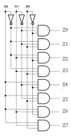
Decoder is a combinational circuit that converts binary information from n input lines to 2^n output lines. It represents the basic calculation of decimal number system from binary number system as mentioned before.
If a binary decoder receives n inputs it activates one and only one of its 2^n outputs based on that input with all other outputs deactivated.
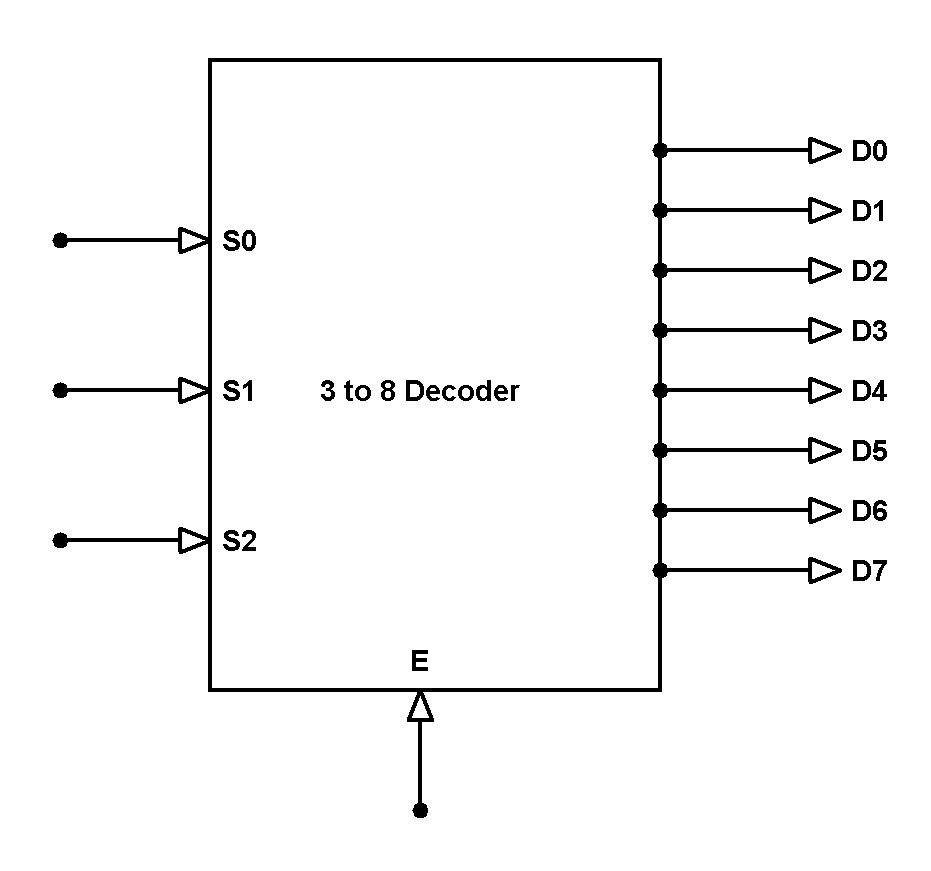
A 3x8 binary decoder looks like this:


The intuition behind it is that the inputs can be supposed to be diiferent input switches and the output lines could be different LED's, so when a combination of input is given through the switches, only the LED with that combination glows and all the other LED's do not glow.
The truth table is as follows:
| S0 | S1 | S2 | E | D0 | D1 | D2 | D3 | D4 | D5 | D6 | D7 |
|---|---|---|---|---|---|---|---|---|---|---|---|
| x | x | x | 0 | 0 | 0 | 0 | 0 | 0 | 0 | 0 | 0 |
| 0 | 0 | 0 | 1 | 0 | 0 | 0 | 0 | 0 | 0 | 0 | 1 |
| 0 | 0 | 1 | 1 | 0 | 0 | 0 | 0 | 0 | 0 | 1 | 0 |
| 0 | 1 | 0 | 1 | 0 | 0 | 0 | 0 | 0 | 1 | 0 | 0 |
| 0 | 1 | 1 | 1 | 0 | 0 | 0 | 0 | 1 | 0 | 0 | 0 |
| 1 | 0 | 0 | 1 | 0 | 0 | 0 | 1 | 0 | 0 | 0 | 0 |
| 1 | 0 | 1 | 1 | 0 | 0 | 1 | 0 | 0 | 0 | 0 | 0 |
| 1 | 1 | 0 | 1 | 0 | 1 | 0 | 0 | 0 | 0 | 0 | 0 |
| 1 | 1 | 1 | 1 | 1 | 0 | 0 | 0 | 0 | 0 | 0 | 0 |
When enable pin is 0 the circuit is not started and when it is 1, the circuit works in the original way.
Similarly there are 2x4 and 4x16 decoders also.
An encoder performs opposite operation to that of a decoder.It has 2^n or fewer input lines and n output lines. Output lines generate binary code corresponding to the input values.
Only one input line should be high and corresponding to that a combination of output lines light up or are generated and the other remain low.
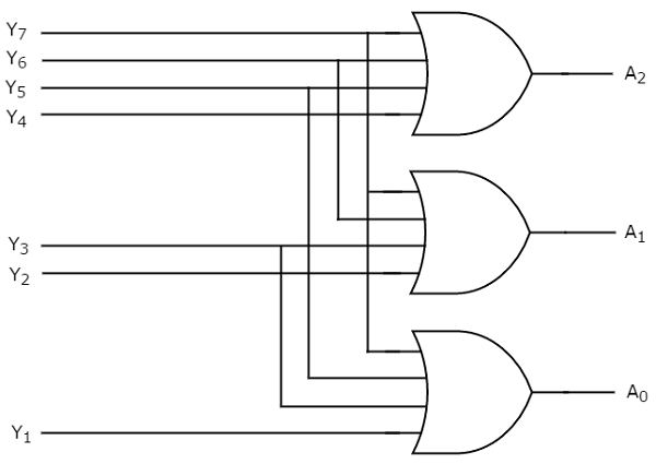
for example an octal to binary encoder: has eight input lines(Y0-Y7) and three output lines(A0-A2)

The truth table for it is as follows:
| Y7 | Y6 | Y5 | Y4 | Y3 | Y2 | Y1 | Y0 | A2 | A1 | A0 |
|---|---|---|---|---|---|---|---|---|---|---|
| 0 | 0 | 0 | 0 | 0 | 0 | 0 | 1 | 0 | 0 | 0 |
| 0 | 0 | 0 | 0 | 0 | 0 | 1 | 0 | 0 | 0 | 1 |
| 0 | 0 | 0 | 0 | 0 | 1 | 0 | 0 | 0 | 1 | 0 |
| 0 | 0 | 0 | 0 | 1 | 0 | 0 | 0 | 0 | 1 | 1 |
| 0 | 0 | 0 | 1 | 0 | 0 | 0 | 0 | 1 | 0 | 0 |
| 0 | 0 | 1 | 0 | 0 | 0 | 0 | 0 | 1 | 0 | 1 |
| 0 | 1 | 0 | 0 | 0 | 0 | 0 | 0 | 1 | 1 | 0 |
| 1 | 0 | 0 | 0 | 0 | 0 | 0 | 0 | 1 | 1 | 1 |
Since, A0 = Y1 + Y3 + Y5 + Y7 , A1 = Y2 + Y3 + Y6 + Y7 , A2 = Y4 + Y5 + Y6 + Y7
However there's one Anomally with an encoder which is if all the ouptut lines are 0 , it could be if all the inputs are 0 or the least significant input is 0.