Recommended Modifications - df8oe/UHSDR GitHub Wiki
All modifications are named according to a scheme. Generally, it is useful to first modify as little as possible, because then you have an easier troubleshooting when something goes wrong.
(WW-XX-Y-ZZZ)
- WW: RF = RF PCB, UI = UI PCB
- XX: PCB Revision
- Y: "N" = modification with normal priority, "H" = Strongly recommended modification
- ZZZ: sequential numbering of all modifications
RF-04-N-001 PA Overshoot
The final PA stage tended to "dynamically overshoot". This meant: depending on drive level, the PA section could in addition to the desired signal emit its own oscillations around 1MHz. Remedy is to install a 10uF tantalum (!!) capacitor in parallel with C106.
RF-04-N-002 PA RX Quiescent Current Reduction
The quiescent current through the two final-stage FET is not shut down safely when the device is in RX mode. The reason is that at the output of the LM2931 a minimum load is required to safely reach the "0V". A solution is to install a resistor 1K-2,2K in parallel to C96. To minimize spurious noise that could spread to the transmission over the PA bias setting C96 is changed from 2.2uF to 100uF tantalum (!!).
UI-04/05/06-N-003 Easily Removable/Replaceable Display
The screen should not be soldered directly. Install two female connectors on the PCB where the display should attach. The bars are not easy to obtain, since the spacing is unusual 2mm. They can be purchased at Farnell under the order 110-9733. To have the height of the display above the ui board not much bigger as it was before (if soldered direct) the two black plastic strips of the two pin headers on the display panel should be peeled off carefully and then the pins themselves should be carefully cut down to about 3 ... 4mm using sharp cutters.
UI-04-N-004 HY28A Display vs. HY28B Display Changes [The model number, is written on the back of the Display]
R30, R31 and R32 (all 0R) do not mount on the UI circuit board, if one has the newer LCD display HY28B. These hinder the possible future use of the touch function of the display panel. If you have the old HY28A, one may only populate the resistors when operating the display in SPI mode, otherwise you disable the touch function.
RF-04-N-005 I/Q Signal Phase Improvement
The phasing of the I/Q-audio signals is changed by a series circuit of capacitors. To minimize, the phase differences in both channels, C71 and C73 are replaced by 0R resistors.
UI-04-N-006 Display Dimming Interference Reduction
The harmonics of the display PWM dimming schemes can cause interference. To minimize this, the electrolytic capacitor C74a is replaced with a tantalum capacitor of equal value. (better is to not use dimming at all because it sometimes generates noise in the received signal)
RF-04-N-007 RX Sensitivity Improvement
The PIN diodes for switching the antenna switch do not have a low enough throughput, thereby the sensitivity of the receiver is reduced. As a remedy, replace R54 with 3.9K, R53 with 220R. (another mod is in development where the switching diodes will be replaced with a relay contact)
UI-04-N-008 Better Power Supply Filtering
Chokes RFC1-RFC3 on the ui board be changed from 4,7uH to 47uH.
RF-04-N-018 RX Sensitivity Improvement
The transistor Q2 and the resistor R40 omitted. The entire receiver scheme has now "disappeared" in the firmware and the sound chip. An assembly of these two components would only weaken the sensitivity of the receiver.
UI-04-N-020 Simplified Bootloader Reprogramming
The two pins of P6 could be extended with a few centimeters of wire and mounted in the housing so that later on you could easily reprogram the bootloader without having to disassemble half of the machine.
UI-04-H-021
is replaced by UI-04-N-025. Those who had already performed this mod, remove the wires, please.
RF-04/05/06-H-029
PIN diode switching often produces spurious TX signals and distorted TX signals. They are only present at some frequencies and not at all TX power levels (so difficult to identify). We have not found any successful modification to the PIN diode switching stage except for removing it and replace it by an "old school" relay switching. Remove RFC2, RFC3, R54, C79, D3 and D4. Apply the following parts:
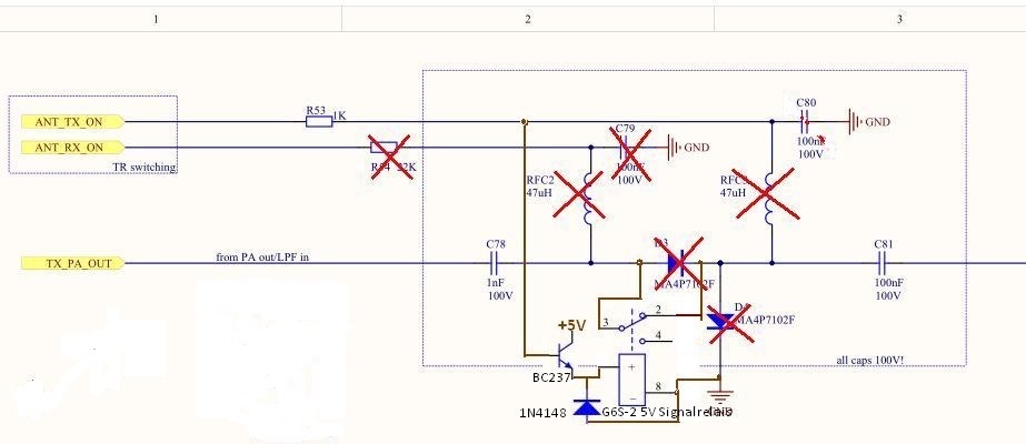 bigger Schematics
If you are in RX mode the Antenna is connected by relays directly to the RX input. If you are transmitting, contacts open and the antenna now disconnects from RX preamp. It is also a good idea to fit two antiparallel diodes (like 1N4148) at position of D4 to prevent preamp input from overvoltage. There are some discussions about IM3 problems using antiparallel diodes. Problems can only occur if antenna signal increases above ~0.5Vss. These are very rare and strange RX antenna levels and do not exist under most circumstances. But we do have more than a few destroyed BFR93A in our German Project group at mcHFs where antiparallel diodes are left out. Check and decide by yourself.
RF-04/05/06-N-023 SWR Meter Operation Improvement
There is a design error in the SWR measuring bridge. The end of the many windings of T3, which currently goes to the RF side of the final stage, has to be pulled from its solder pad. Next to it is the "correct" line: the MAIN PAGE of the bridge that goes to the BNC connector. You can scrape the conductor next to the toroids and now solder the pulled end of the wire there. This SWR measuring bridge is reliable throughout the operating range of the MCHF.
AG-xx-N-024 Recommendation for connector placement on RF/UI Board
To make it possible to exchange boards with other users, we should agree on a consistent use of the male and female connectors. We propose the use of the female connector (socket header) on the RF board and using the male connector (pin header) for the UI board. (that way you have no power pins but power in sockets ... and it is not easy to short them)
UI-04/05-N-027 Keyer Input Line ESD Protection Improvement
To prevent damaging the STM32F4 with static (dis)charges on the keyer lines and on the PTT line two zener diodes of 3.3v should be connected at those lines towards ground. These signal lines can be found on pin 12 and 13 on the ui board (and the diodes can be directly soldered to the board at those pins)
RF-04/05/06-N-009 PA Self Oscillation Prevention
The two gate resistors R81 and R82 were of 220R can be reduced to 100R (only if the amplifier has self oscillatiion at high output levels).
RF-04/05/06-N-010 Reduce Ripple coming from NF PA
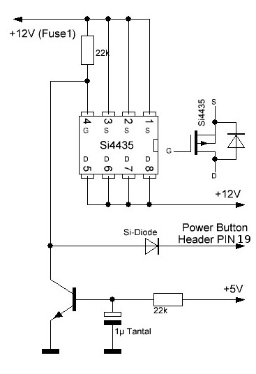
At high speaker volume, the ripple of the 8V supply voltage coupled to the receiver mixer. Why is the NF-amplifier connected to the stabilized voltage? It can be connected directly to the 12V input voltage with a FET. Current change caused by higher volume levels now no longer influence the regulated voltage for the internal receiver stages.
Additionally, I have connected this switched 12V input to the 8V voltage regulator and the two voltage divider elements directly to the 12V. As a result, the quiescent current consumption in "off" mode has now fallen to less than 1uA. (THIS IS THE POWER OFF MOD!)
The following changes are necessary:
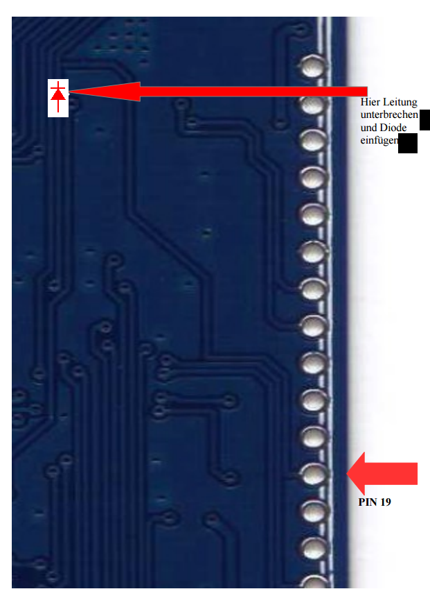
- On the ui board find the line "PC13" from the processor to the power switch and the header below the LCD . The line has to be cut and a diode has to be added in this line (anode to the processor out) (now you know why not to solder the screen direct to the board!! this mod is behind the display)
- On the rf board de-solder and pull up Pin4 from U3, and also pull out of the board the sides of R9 and R13, which will go to 12V. (solder the resistors vertical on the board so the second side stays free in the air) ... These three connectors are now merged with wire and attached to SW_12V of the new circuit.
- The rest will be seen from the unique labels of the new circuit diagram. On the right, you can see the place where the additional diode is installed. The site is located on the ui board below the LCD. The cathode of the diode is then seen in the picture in the above position, and the anode (for STM32F4 out) is seen in the lower position.
Here are the required pictures
UI-03-N-001 Adding EEPROM on the old UI Board Rev. 03
If you have old UI board (rev. 03 and older), and want that new features of recent FWs to works fluently, you have to add an additional EEPROM to it. EEPROM should be located just above C73 (see attached link). You can use two EEPROMs, both 1Mb, 24LC1025 or newer 24LC1026. Because they have minor differences inside, please follow instructions below: Be aware that this modification is suitable for UI Board Rev. 03 or older only!
Using EEPROM 24LC1025:
- Cut off pins 1 and 2.>>>
- Bend pins 3, 5, 6 and 8 straight out. >>>
- Solder pins 4 and 7 on surface (GND). >>>
- Solder SMD capacitor 100nF between pin 3 and GND (surface). >>>
- Connect pin 5 to R22 and pin 6 to R21. >>>
- Connect + pole of C17 to pins 3 and 8.
Using EEPROM 24LC1026:
- Cut off pins 1, 2 and 3. >>>
- Bend pins 5, 6 and 8 straight out. >>>
- Solder pins 4 and 7 on surface (GND). >>>
- Solder SMD capacitor 100nF between pin 8 and GND. >>>
- Connect pin 5 to R22 and pin 6 to R21. >>>
- Connect + pole of C17 and pin 8.
EEPROM on UI Board Rev. 03 EEPROM pinouts
RF-04-N-011 Reduce standby current
The standby current is not switched by PTT and flows also when the mcHF is switched off. To switch the standby current with the PTT, the following modification around Q3 and Q4 must be done:
- Change R74 and R76 from 470R to 2.2K
- remove R73 and R75
- solder R73 and R75 upright on the pad that is connected to the base
- solder a 100nF capacitor upright from the ground-base of R79
- connect the three upright parts (R73,R75,100nF) with U2, pin1 (PTT_5V)
RF-04-N-012, RF-04-N-022 Correct unsymmetrical ADC in the SWR measurement
Due to unsymmetrical ADC converter and the leak of firmware, correction of the SWR circuit needs some changes to work properly:
- Replace R59 and R60 with 0R (former value 1K)
- Change R58 and R62 from 100K to 2.2K
- Change C82 and C83 from 100nF to 2.2uF
Please also have a look at RF-04-!-023
AG-xx-N-013 Shield between the boards
The clock signal on the UI board can interfere the RF board. To minimize this, an isolated copper foil should be installed between the boards. The foil can be wrapped around the board.
FW-xx-N-014 SI570 autodetect
There are different SI570 versions available. The actual firmware will automatically check the startup frequency and the I2C address. Check the firmware on the github
RF-04-N-015 Replace T5
To increase the TX power replace T5 with an self build transformer based on a BN43-2402 core. The primary winding is 5 turns CuL 0.3mm, the secondary winding is 4 turns CuL 0.3mm with a centre tap connection. Please check also the document from IZ6MAF in the Yahoo group IZ6MAF mcHF RF TX SWR notes. I cannot confirm improvements with modified output transformers compared to original solution.
RF-04-N-016 Replace RFC5 and RFC6
Replace the feeder inductors RFC5 and RFC6, using a BN43-2402 with 4 turns CuL 0.3mm to increase the TX power
UI-04-N-017 5V on USB to use USB for firmware updates
OBSOLETE. DF8OE bootloader 2.0.x now uses the large USB connector which by default is powered. This modification is kept for reference only.
Firmware updates can be done via USB. The Mini-USB connector must be deliver 5V:
- Connect the 5V side of R45 through a Schottky-Diode with the 5V PIN of the USB-OTG connector
- For safety reasons is is recommended to install a fuse (or polyfuse) within this connection
- Connect a 100uF/6V tantalum capacitor from the 5V pin of the USB connector to the ground
Please note that the DF8OE bootloader must be installed to use the USB firmware update github. There are problems with some USB sticks. Best results are known with 2GB sticks working stick
UI-04/05/06-N-019 Fit/Replace U7 EEPROM
The use of an I2C EEPROM to store the configuration is strongly recommended. If no appropriate EEPROM is found, the flash is used instead for saving the configuration, but be aware that it will cause the mcu to wear out after longer usage of the internal flash! So better install a large enough I2C right now!
Please note, that the EEPROM must be new or filled with 0xFF completely.
Too small eeproms are not going to be used by the firmware (see System Info menu).
The U7 24LC01 eeprom is too small to store the configuration.
There are different types you can install instead:
- 24LC1025
- 24LC256 (32kb) 24LC512 (64kb), 24LC1026 (128kb) and AT24CM02 (256kb)
mcHF UI Revision 0.4 AND 0.5
This is only valid for rev 0.4 and 0.5!
Layout on board is prepared for all EEPROM but 24LC105.
- 24LC256 (32kb) 24LC512 (64kb), 24LC1026 (128kb) and AT24CM02 (256kb) : all these can be be fitted to board without changes on 0.4 and 0.5 boards
- 24LC1025: You need to install a connection between pin3 and pin8 on rev 0.4 and 0.5. Pin 3 must not be connected to the solder pad for pin 3.
mcHF UI Revision 0.6
This is only valid for mcHF PCB rev 0.6
- 24LC1025: can be be fitted to board without any additional changes
- 24LC256 (32kb) 24LC512 (64kb), 24LC1026 (128kb) and AT24CM02 (256kb) : for all these you must desolder pin3 and tie it to GND i.e. pin2 or pin4
The 24LC1025 is easy to fit on the backside of the UI Revision 0.6 board and is the soic8 type.
UI-04-N-025 / UI-05-N-025 / UI-06-N-025 Switch LCD to SPI mode (Optional, please read the newsgroup)
By default the UHSDR software supports both HY28A and the newer HY28B (sold after 01/2015) in parallel mode.
This modification is about using the displays in SPI mode. Be aware that both schematics, 0.4 and 0.5 UI, show a HY28A, 0.6 shows a HY28B. The SPI connections of an HY28B are on different pins compared to the HY28A on the display (16 - SDO, 17 - SDI, 13 - SCK).
Setting SPI Mode on the HY28A / HY28B Display
HY28B Display SPI Mode Settings
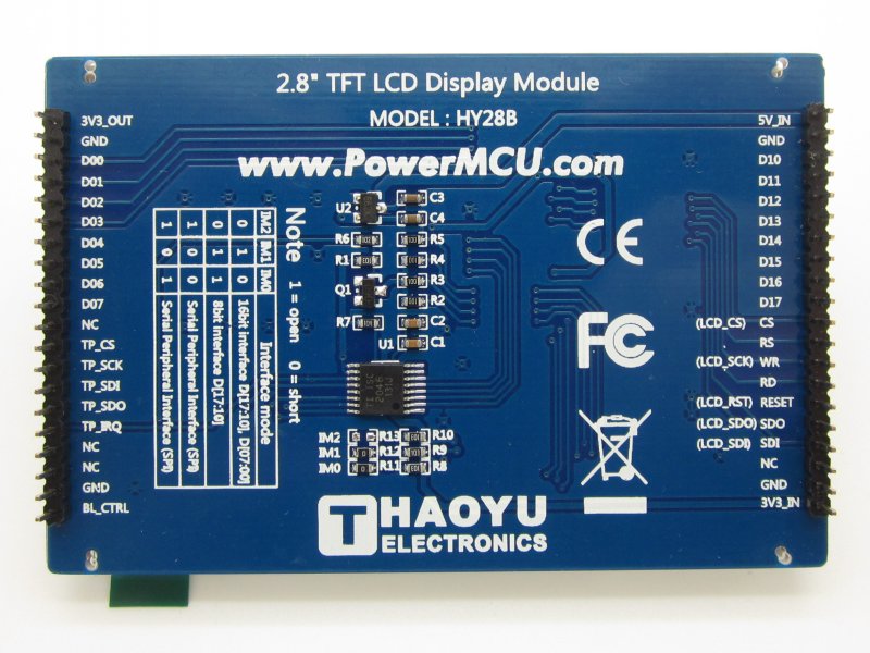
Remember to set the jumpers IM0 - IM2 on the display correctly: IM0 and IM1 are closed, IM2 is open as shown on the image below:
HY28A Display SPI Mode Settings
The HY28A display are fixed to be either SPI or parallel.
Routing the Display SPI to the MCU
UI 0.4 HY28B
This modification is about using the HY28B (!) displays in SPI mode on a rev 0.4 UI board.
R30-R32 MUST NOT be fitted. Remove them if soldered, these are only for HY28A displays in SPI mode. You will get a white screen with the HY28B and these resistors fitted with any recent firmware. Very old firmware may work since they do not use the SPI for touch screen.
- connect R30/R33 to LCD pin 16 (SDO)
- connect R31/R34 to LCD pin 17 (SDI)
- connect R32/R35 to LCD pin 13 (SCK)
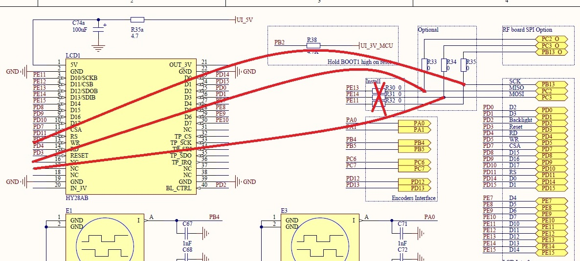
UI 0.4 HY28A
This modification is about using the HY28A (!) displays in SPI mode on a rev 0.4 UI board.
The PCB layout is prepared to support the SPI mode for the HY28A display. Just solder 3 0R resistors to R30 - R32.
UI 0.5 HY28B/HY28A
This modification is about using the HY28B or HY28A (!) displays in SPI mode on a rev 0.5 UI board.
If the touchscreen SPI is enabled, i.e. R30 - R32 are fitted, it does not matter on wich side you connect the wires from the HY28B/HY28A pins. Otherwise you have to identify the pad which goes to the MCU and not to the display.
- connect R30 (side to MCU) to LCD pin 16-HY28B /5-HY28A (SDO)
- connect R31 (side to MCU) to LCD pin 17-HY28B /6-HY28A (SDI)
- connect R32 (side to MCU) to LCD pin 13-HY28B /3-HY28A (SCK)
This will be used in future to get some more GPIO pins for further enhancements. There are big advancements in the speed of SPI mode in the last months. This change is (not yet) necessary.
UI 0.6.0 HY28B SPI
This modification is about using the HY28B (!) displays in SPI mode on a rev 0.6.0 UI board (starting with 0.6.1, only SPI is supported and no modifications are needed).
The PCB layout is prepared to support the SPI mode for the HY28B display. Just solder 3 0R resistors to R30a, R31a, R32a.
It is recommended to remove R32b-R32e and R32g-R32u (NOT R32f - this is the SPI LCD CS), this disconnects the parallel mode pins for use e.g. for the RTC mod.
UI-04-N-026 Activate touchscreen (recommended to use actual FW features)
To use the touchscreen five wires must be connected. It is very important to remove the resistors R30..R32
- connect PA4 MCU to LCD TP_IRQ
- connect R30/R33 to LCD TP_SDO
- connect R31/R34 to LCD TP_SDI
- connect R32/R35 to LCD TP_SCK
- connect PA9 MCU to LCD TP_CS
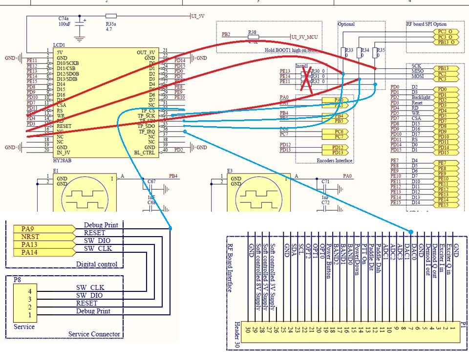
Please note, that the RED wires are only necessary to use SPI with LCD (see UI-04-N-025)
UI-05-N-026 Activate touchscreen (recommended to use actual FW features)
Touchscreen implementation on board 0.5 is incomplete and in some places not compatible with the firmware. On board 0.5 you must modify the ui board:
- fit R30...R32
- remove R33 and R34
- don't fit R47b and R47d
- put a wire between R33(side to LCD) and R47d (side to MCU)
- put a wire between R34(side to LCD) and R47b (side to MCU)
UI-04/05-N-031 Enable STM32 Real Time Clock
This modification allows the use of an integrated real time clock which runs even if the mcHF is powered off. It is a simple modification which requires serious soldering skills and tools.
Prerequisites: Your mcHF MUST use SPI display mode, since we utilize 2 GPIOs from the parallel data lines of the display (which are unused in SPI mode). All HY28B are capable of the SPI mode, see above. HY28A and other displays may not support parallel to SPI switching.
The change will make your hardware incompatible with older firmware (reversible!) since 2 buttons will be connected to the above mentioned display GPIOs. The modification is semi-automatically detected by newer firmware (1.5.8 or newer). Older firmware will give you the blue key test screen with 300 as initial keys if you run it with the completed modifications.
This modification requires some extra hardware:
- A 32768 Hz crystal including capacitive loads (recommended Microcrystal MS3V-T1R 32.768 kHz, 12.5pF load)
- A 3V battery (e.g. CR2032) with a battery holder or with solder tabs)
Part 1: Battery support for backup data and clock.
- Upload the newest daily build firmware if not done before. Make sure it boots.
- Remove C82
- Cut 3.3V trace going underneath C82 to the C82+ solder pad. Make sure to cut only this trace!
- Test continuity between 3.3V and C82+ pad. There should be none.
- Solder 2 wires to the pads and to the battery tabs or holder. Check polarity!!!
- Now turn on the mcHF twice (!) and go to System Info Menu. It should show "Backup RAM Battery" as "Yes" and "Real Time Clock" as "N/A". If not, check the wiring. Do not proceed until this works.
Part 2: Button rewiring
- cut the traces coming from pins PC14 and PC15 so that there is enough trace towards the STM32 to solder the two tiny legs of the crystal. PC14 is connected to M1 and PC15 to F3. Test continuity before and after cutting to make sure you cut the right traces. The traces run directly beside C82. One is directly under one of the C82 solder mask lines, the other directly beside this one.
- Scratch off solder mask from the traces on the STM32 side of the just cut made so that you will be able to solder the crystal legs to these. Do not solder the crystal yet! See image below.
- Use two wires to connect the M1 and F3 buttons to D0 and D1 of the LCD, see image below.
- Start mcHF and verify the buttons are NOT working anymore. That is good. These buttons will get back to life once your mcHF clock is running.
Part 3: Crystal goes in
- Take the crystal and bend the legs so that these have same distances as the two traces.
- Solder crystal to traces. The crystal body faces downwards, see image below.
- Carefully scratch off some solder mask from the ground plane right at the end of the crystal body. Put some solder on it and solder crystal body to the ground plane. Be careful to not put too much stress on the tiny legs in order to keep the traces sticking to the PCB. Once the body is soldered using enough solder, this connection will prevent mechanical stress on the legs.
Part 4: Enabling RTC.
- Boot with the crystal soldered in.
- Go to "Expert/Debug Menu"
- Select "RTC Start". Your mcHF will reboot.
- After reboot, if the mcHF will not work anymore (Green LED, but black screen only), the quartz is not working. Remove battery and power. Next start will get you back into the initial mode, buttons M1 and F3 will not work but the rest should be fine. Figure out what goes wrong and try again.
- If the RTC was successfully enabled, you will see the clock on screen. Menu items to change the time are currently located in the Debug Menu and will only be visible if the mcHF detected battery support for the real time clock.
Undoing the modification
If you remove the battery, the firmware will automatically assume that your hardware is unmodified. You need to reconnect M1 and F3 to PC14 and PC15. There is no need to remove the crystal, it will not harm the radio. If you remove it, you can use solder bridges to reconnect it, otherwise simply use wires.
You may also use the menu item "RTC Reset" to disable the RTC function and reset it to the default state. Rebooting the mcHF will start the process as if the battery has been installed for the first time.