Unit 3 Memory Roadmap - birdybro/Nand2Tetris_MiSTer GitHub Wiki
This module is about building the main memory unit. We build flip flop gates, one-bit registers, and then n-bit registers. Different from the previous 2 steps where everything was combinational logic, We will get into clocked sequential logic as well.
Unit 3.1 - Sequential logic
Time to deal with time :) this is an area I kinda need to round out knowledge on so I look forward to it. There's state management basics in here too. He shows an example of a for loop sort of (it's actually misleading to think of for i = 1 .. 100 as a for loop imo in hdl, it's more like another more complicated abstracted boolean algebra sorta? but i guess software it's the same when whittled down at the end of the day right?).
Clock goes up and down at a fixed rate, each cycle of it going down and then up is counted up as a time unit, so clk 0 --> 1 = time(1), then again clk 0 --> 1 = time(2). Looks like I'll have to make a "ticktock" file of sorts as a first step? Not sure yet.
Unit 3.2 - Flip Flops
state[t] = function(state[t-1]) - this is a nice summary of sequential logic.
Flip flops basically "flip" between two states, thus they are capable of storing a value. He shows an example of how to do a 1-bit register that changes on the cycle after a load signal has been received. Seems pretty straight forward, you would use a Mux and you would tie the output of the dff to the 2nd input of the mux and the 1st input is the signal you want to capture if you change, and load is the clock enable.
Unit 3.3 - Memory Units
Memory in this context can be Cache/RAM/etc..., Disks/memory sticks/etc..., volatile/non-volatile, etc... RAM is for data and instructions.
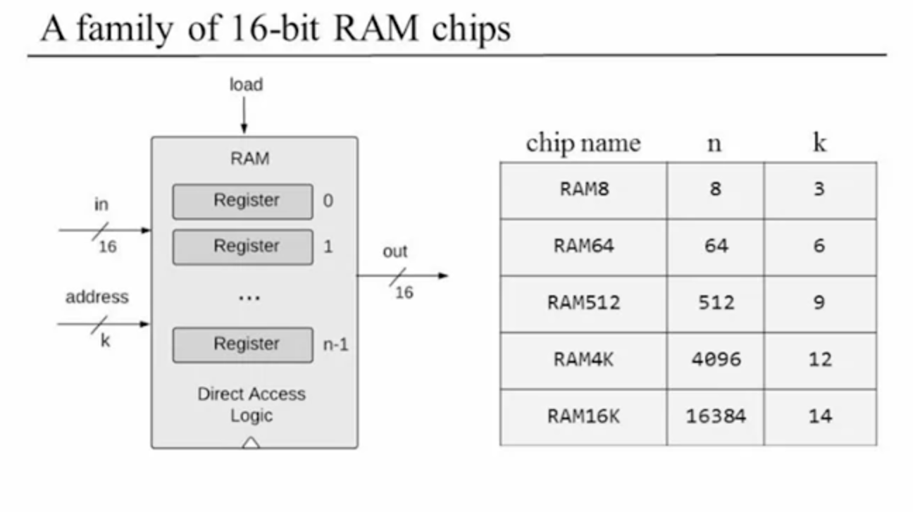
He gives a demo of the simulator again but with the builtin DRegister (Clocked) chip. Overall pretty simple. These are the memory chips we are going to make in this unit:
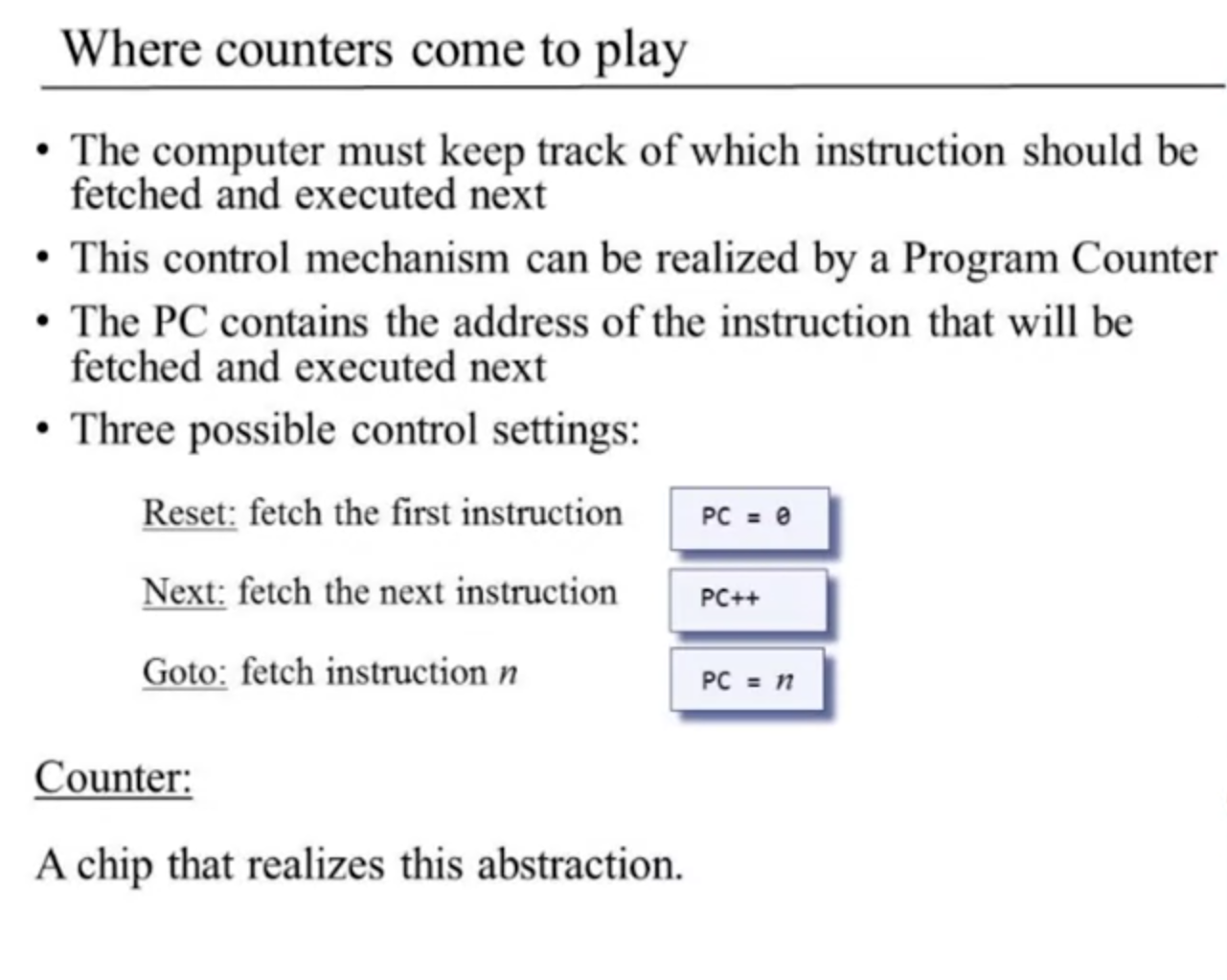
Unit 3.4 - Counters
Pretty good summary of a counter:
Here's the design that I have to come up with:
Unit 3.5 - Project 3 Overview
We are given all chips from projects 1 and 2, and then we are also given a Data Flip-Flop (DFF Gate). The goal is to build the following chips:
- Bit (1-Bit)
- Register (16 1-Bits)
- Ram8
- Ram64
- Ram512
- Ram4k
- Ram16k
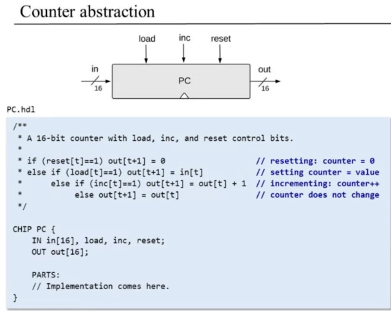
- PC (Program Counter)
Some implementation tips:
- 1-bit register = built from a DFF and a Mux
- 16-bit register = build from 16 1-bit registers
- 8-Register RAM = Feed the
invalue to all the registers simultaneously. Use mux/dmux chips to select the right register. - 64-Register RAM --> 16k-Register RAM = Start with RAM8 and put 8 of them together to make a RAM64, then do 8 RAM64s to make a RAM512, etc... All the way up to RAM16k. A RAM device can be built by grouping together smaller RAM parts. Think about RAM's address input as consisting of two fields:
- One field can be used to select a RAM-part.
- The other can be used to select a register within that RAM-part.
- And you use mux/demux logic to effect the hierarchical addressing scheme for the 64-Register --> 16k-Register RAM chips.
- Program Counter (PC):
- load = when high load the value from in[15:0] at each tock
- inc = when high count + 1 each tock
- reset = when high resets to 0 at each tock
- You can use a register chip, incrementor chip, and some other logic gates to make the PC chip.
Best Practice Advice like before, but also:
- Use the built-in chips because you are submitting them to the course.
- keep the two directory structure as is (
aandb).
Conclusion
Passed with 100% score! :)