Inspecting Your Mainboard - betrusted-io/betrusted-wiki GitHub Wiki
Before using your device, you may want to have a look at the mainboard to ensure its correct construction. The disassembly guide for installing the failsafe programming cable might be helpful to determine how to gain access to inspect the motherboard.
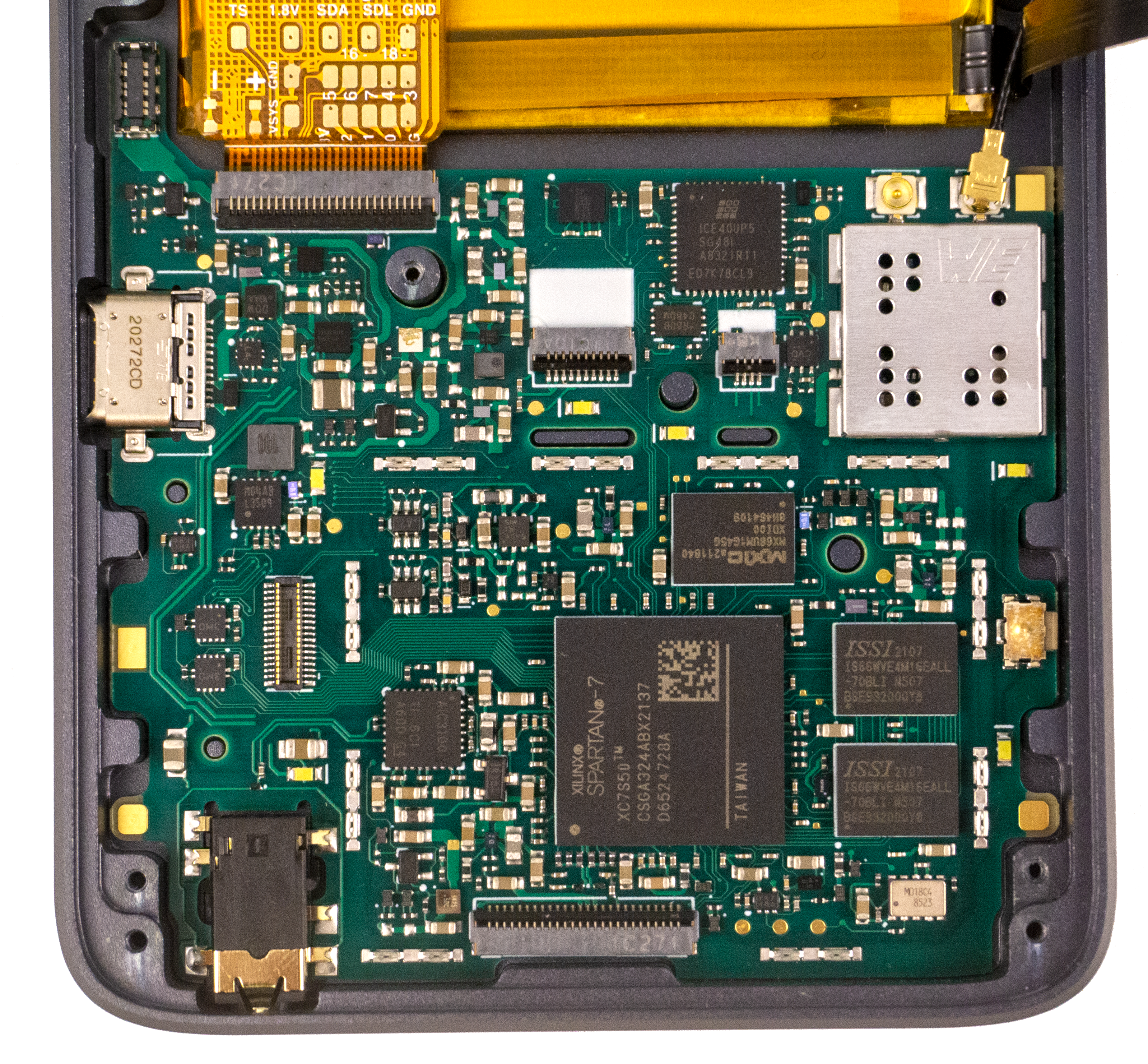
Here is an overview of the components on the mainboard, along with schematics.

Trusted Domain Point-by-Point
That's a lot of detail, so we've created a point-by-point guide of the "trusted domain" and the regions to look at, and why they are interesting.
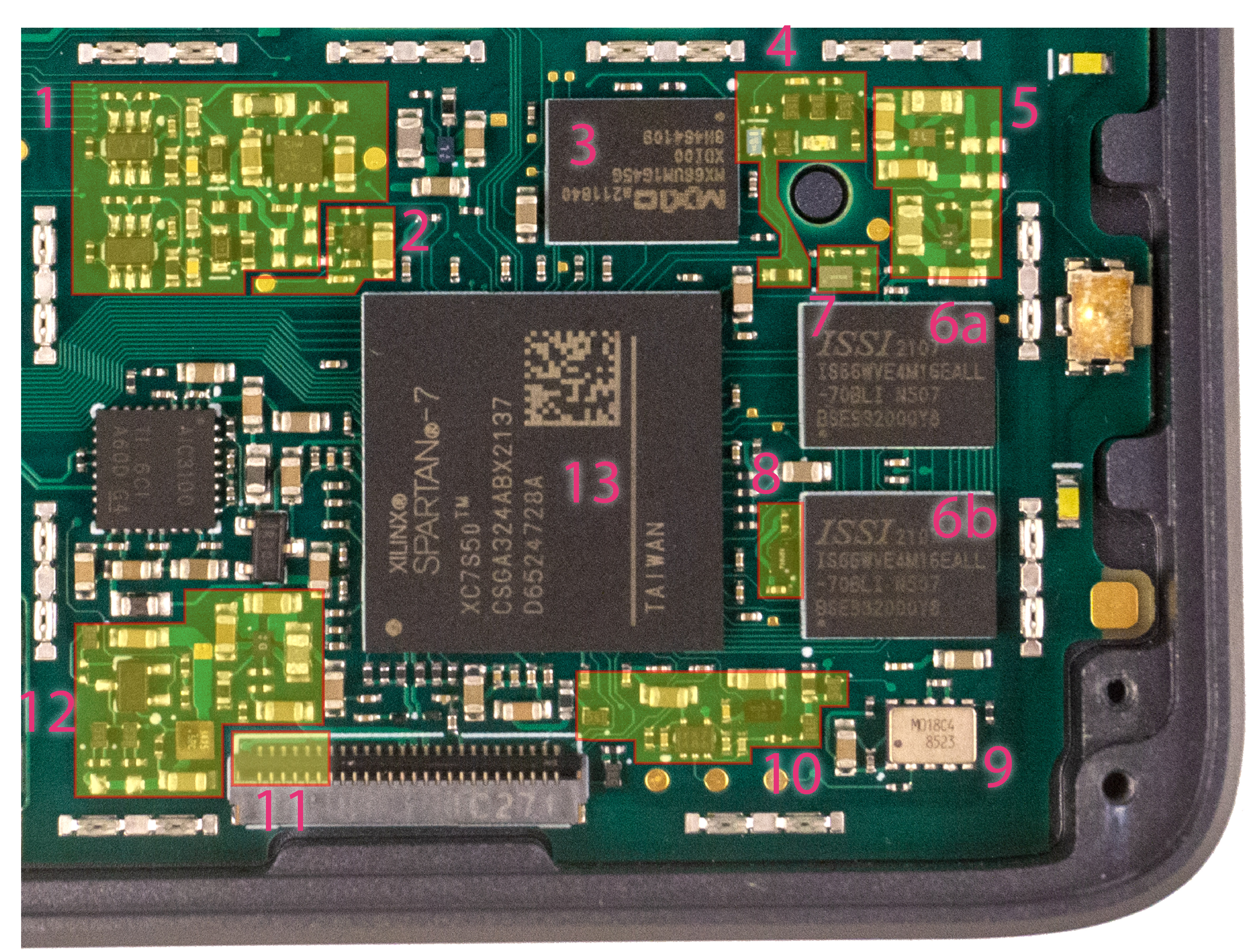
- Avalanche generator TRNG source. There are two noise sources operating in parallel powered by a single boost supply in this circuit. While there are continuously running statistical tests to ensure it is operating properly, modifications to this can greatly impact security properties of the underlying software.
- Battery-backed AES key regulator. The test point on the left edge can be used to defeat the self destruct mechanism.
- FLASH memory. The part number should be MX66UM1G45G. When examined under X-ray, you may see two stacked die inside. This is normal.
- AES kill key latch. This is a discrete circuit that shuts down the battery backed AES key regulator and battery-backed RAM supply in the event of a self destruct. The red LED will turn on when this is activated. The circuit will not de-activate until the battery voltage is removed.
- 1.8V domain regulators. They supply power to the RAM and on-chip block RAM on the FPGA. Glitches here can corrupt OS state.
- (6a & 6b) SRAM chips. the part number should be IS66WVE4M16EALL-70BLI
- SRAM ZZ isolation circuit. This is normally used during standby to prevent RAM corruption, but can be abused in normal operation to intentionally corrupt RAM.
- SRAM CE isolation circuit. This is normally used during standby to prevent RAM corruption, but can be abused in normal operation to intentionally corrupt RAM.
- RTC module. The markings on this module unfortunately are not fully specified by the vendor.
- Power glitch & active discharge circuit. The circuits here will reset the SOC in case of a power glitch on the power that feeds the self destruct circuit, and there are also FETs that actively discharge the power rails so in case of a shutdown it is rapid and complete.
- JTAG pins. Any Starbleed/WBSTAR exploit would require access to this bank of pins in particular.
- SoC core voltage supply and mains switches. Glitches on the core voltage supply can disrupt SoC function.
- Main FPGA that implements the SoC function. The part number should be XC7S50.
There should be no additional fly-wires or components present beyond the ones visible in this photo.
An unmarked version of the reference image can be downloaded here.
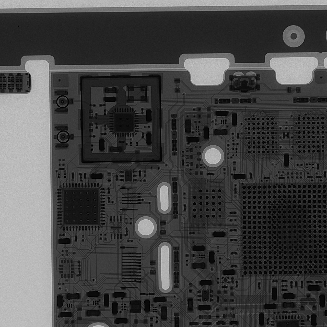
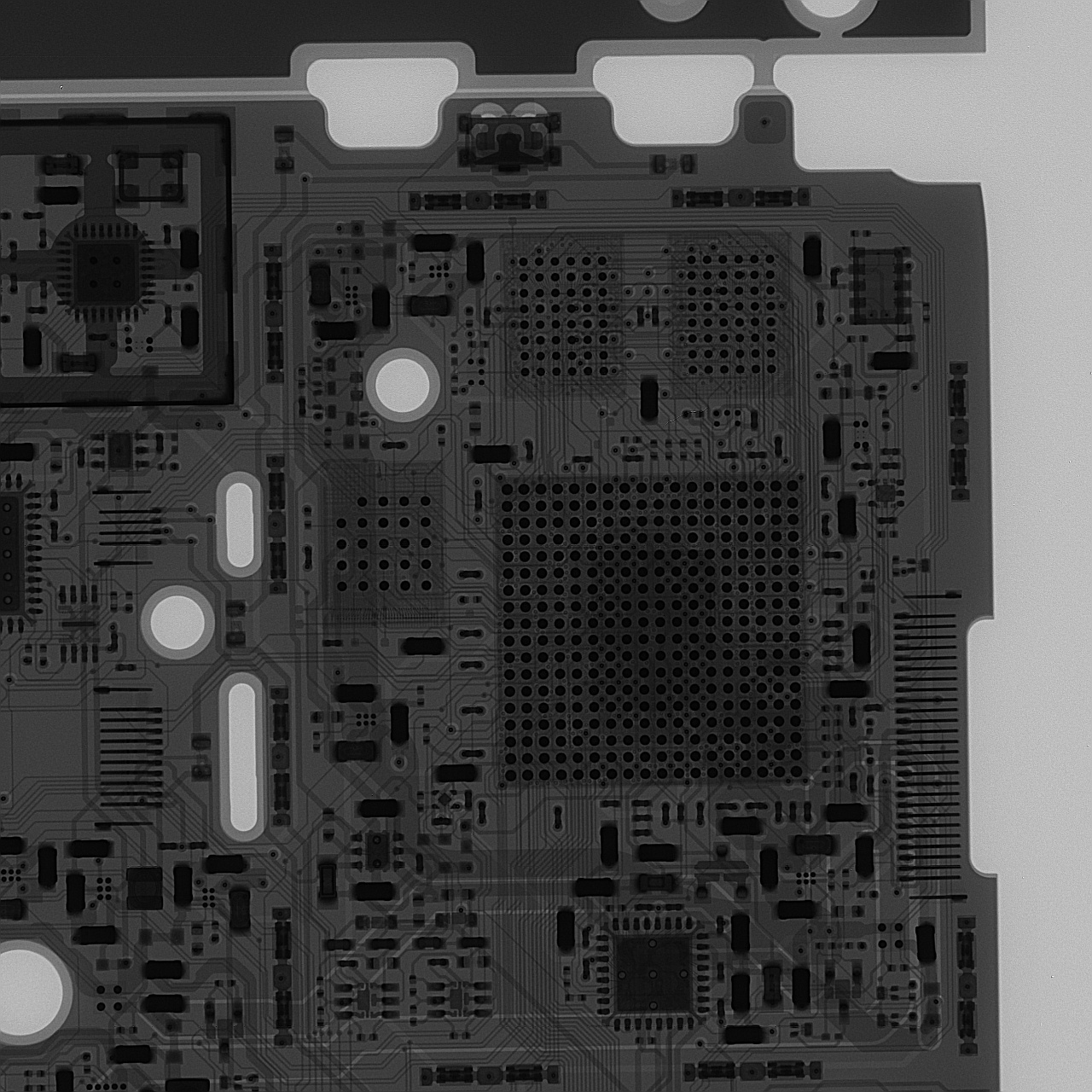
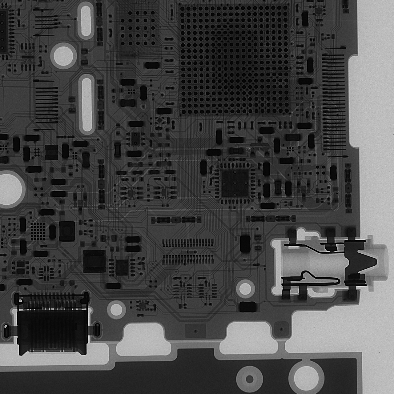
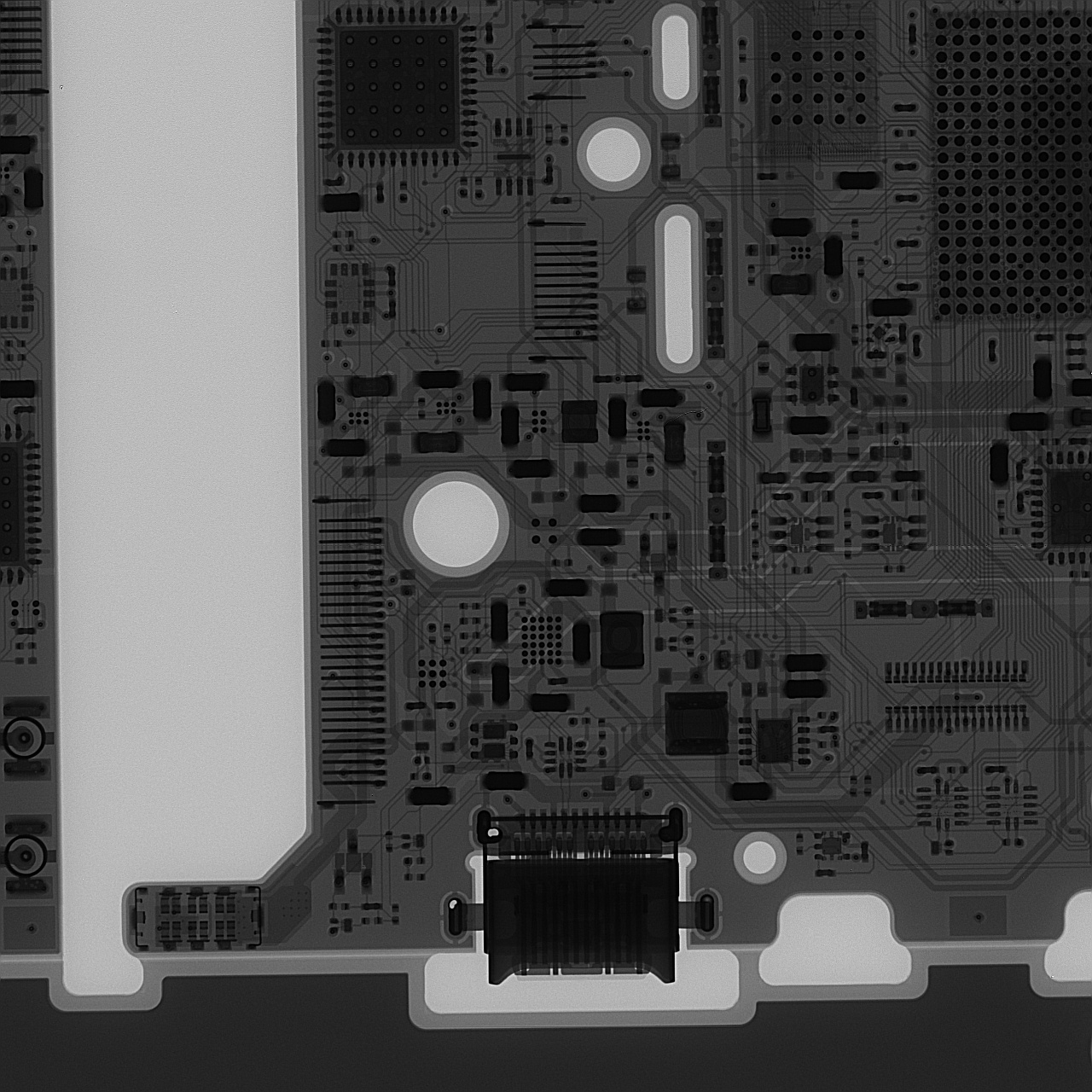
X-Ray
For those fortunate to have access to an X-ray machine, here are some reference images of a near-final production board.
You will note that silicon basically transparent to X-rays, so you will need to pay attention to the location of bond wires to infer the dimensions of the chip inside the packages. Note that vendors are allowed to and frequently do shrink or swap out chips to optimize their supply chains.