Pico v0.3 0.4 - alanbjohnston/CubeSatSim GitHub Wiki
Building the CubeSatSim Pico
These are the instructions for building the Pico Board, Batt Board, and Solar Board.
Here is the software for the CubeSatSim Pico: https://github.com/alanbjohnston/CubeSatSim/tree/pico/cubesatsim
Pico Board v0.4
These are the instructions for building the Pico v0.4 board.
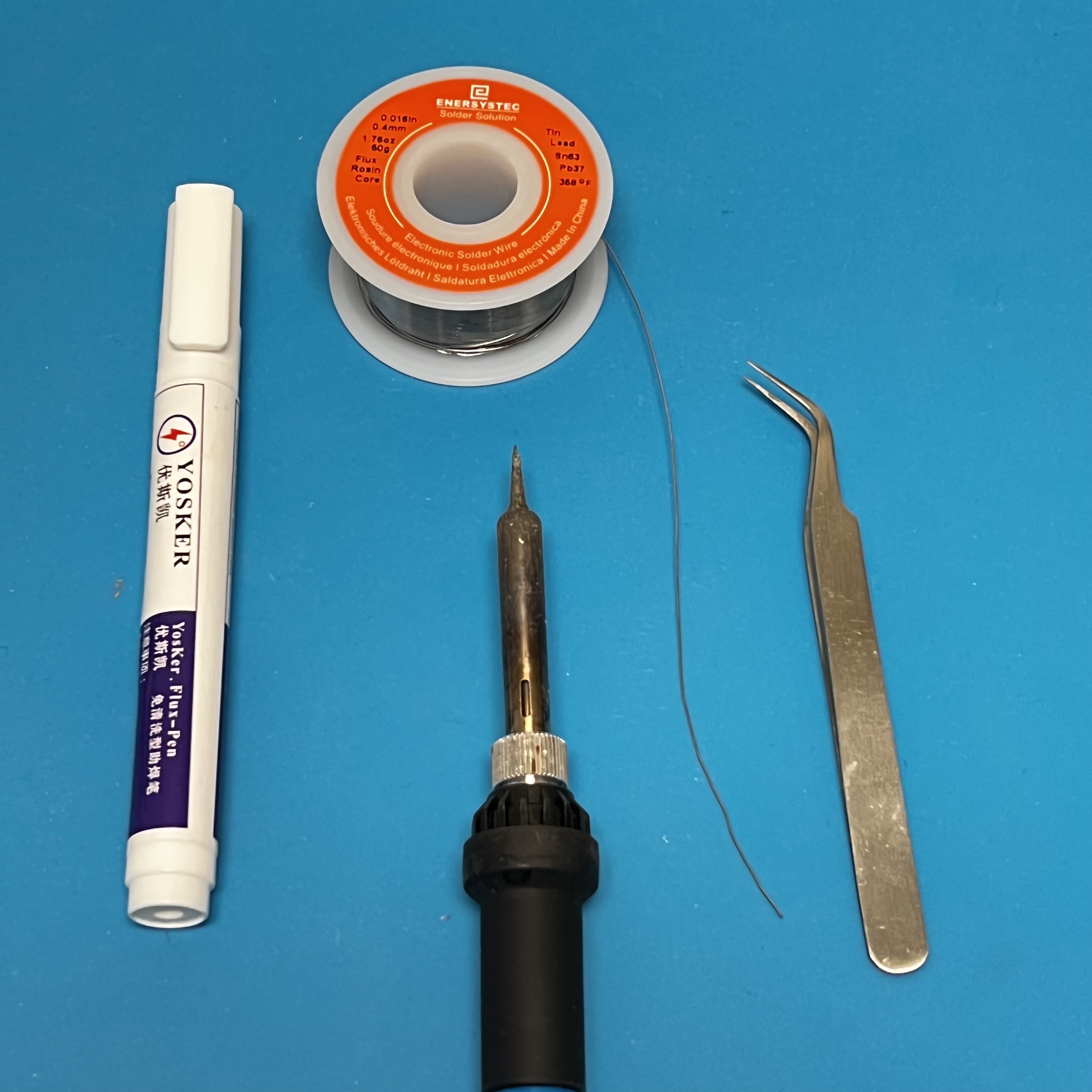
You will need these tools:
- Safety glasses (to protect eyes while soldering or trimming leads)
- Soldering iron with fine tip and very thin solder (I use lead-free solder, but leaded solder is easier to work with)
- Flux pen
- Tweezers
- Needle nose pliers (to bend leads and hold parts)
- Side cutters (to trim leads)
Other tools that are helpful:
- Blue mounting putty (to hold components in place while soldering)
Checklist
The BOM has a sheet "By Steps" which lists the parts needed for each step in order. https://docs.google.com/spreadsheets/d/1ByTG41r7f3VARUdgwTEE2agh6ibNvTtx3HnqygkxIfs/edit?usp=sharing If you have a Google account, you can make a copy of this spreadsheet ("File" then "Make a Copy") and check off each part as you install it.
For example, here is the checklist for this step (TBD).
Assembly
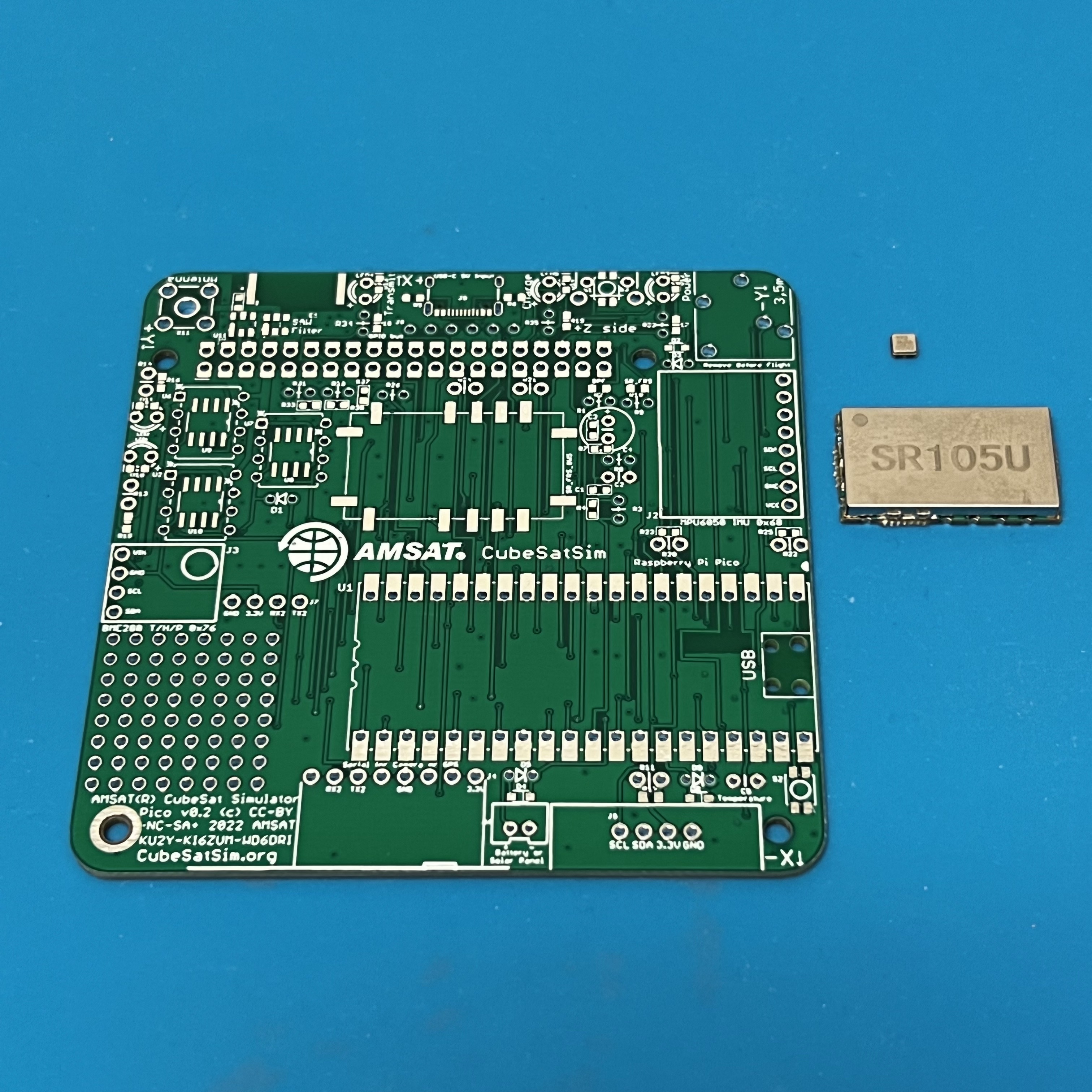
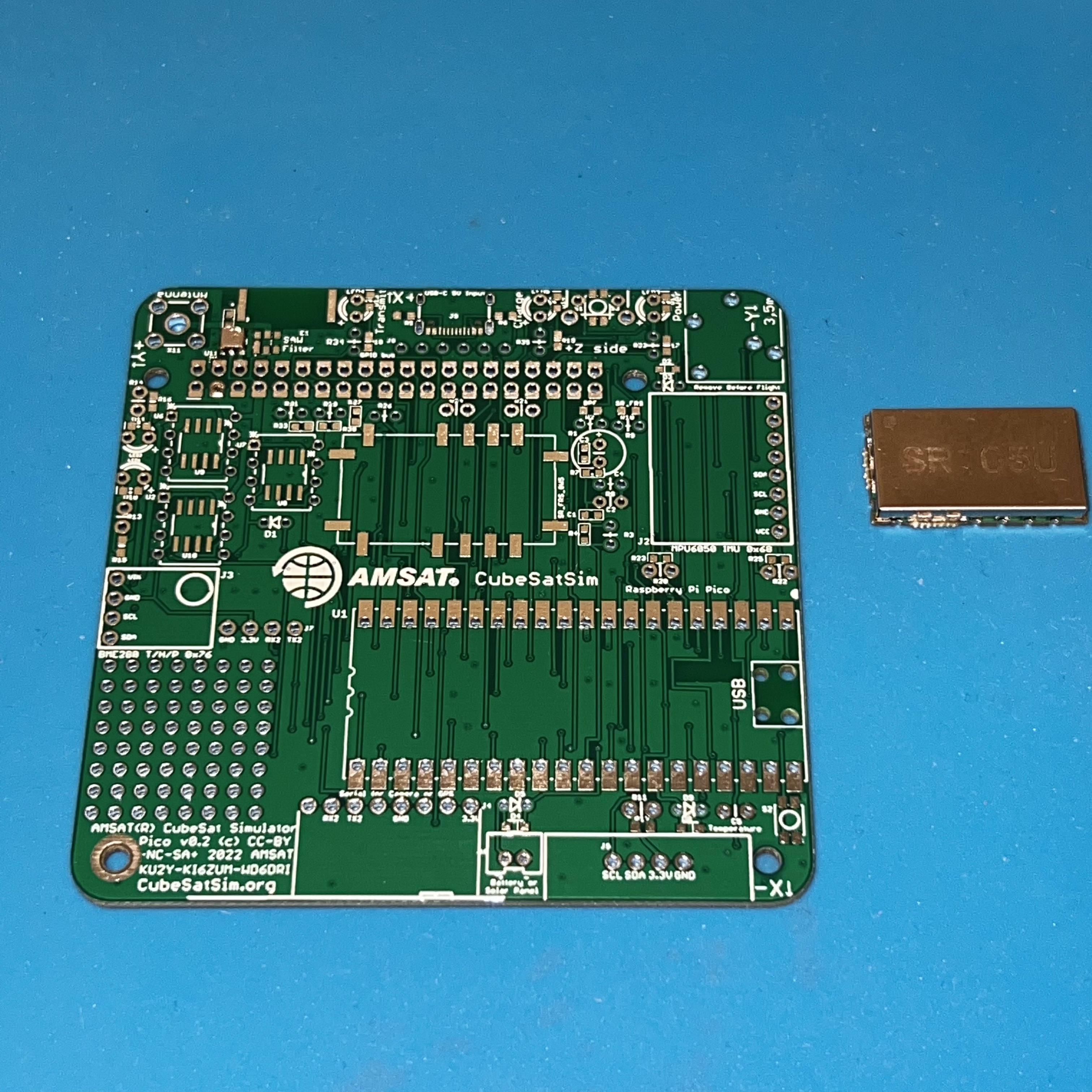
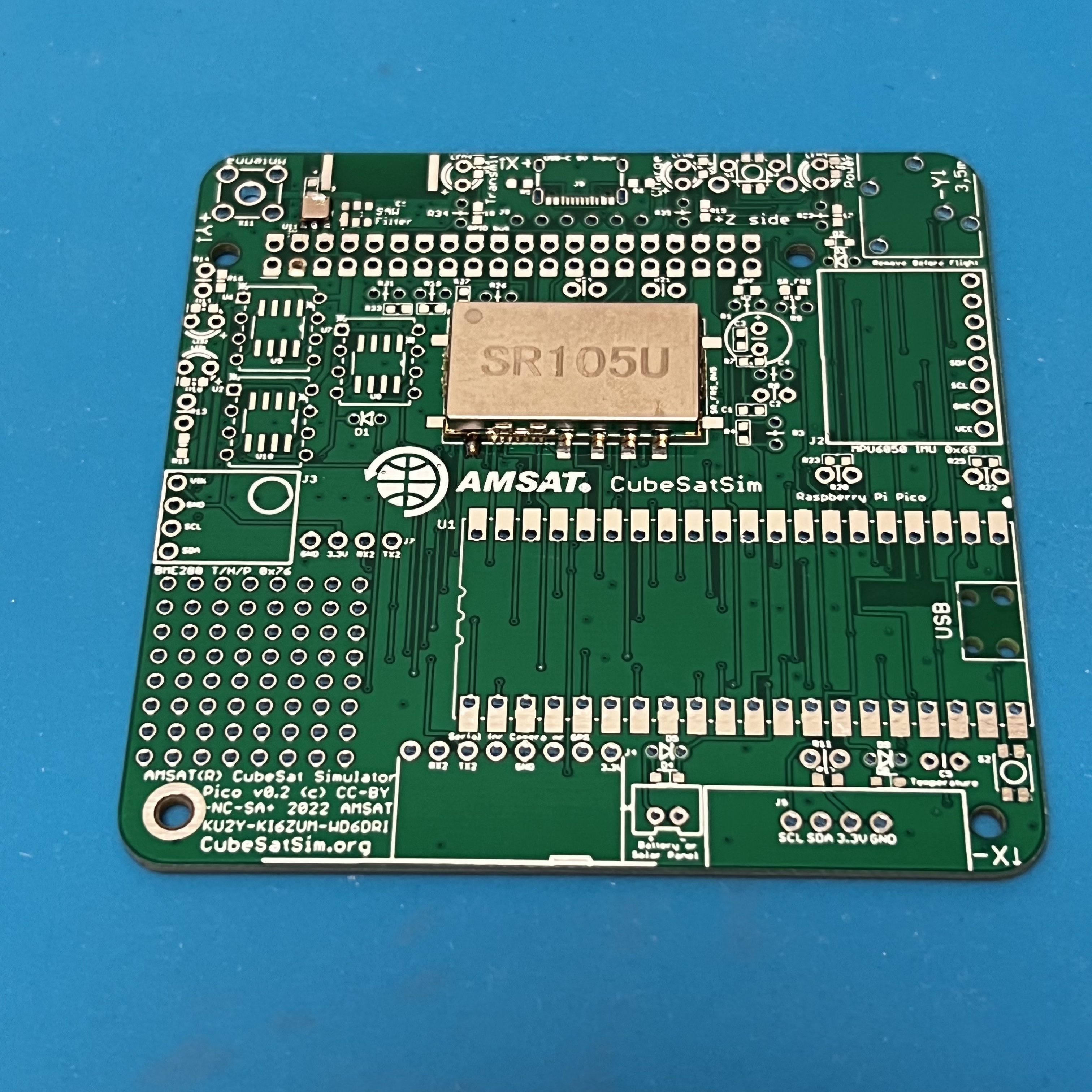
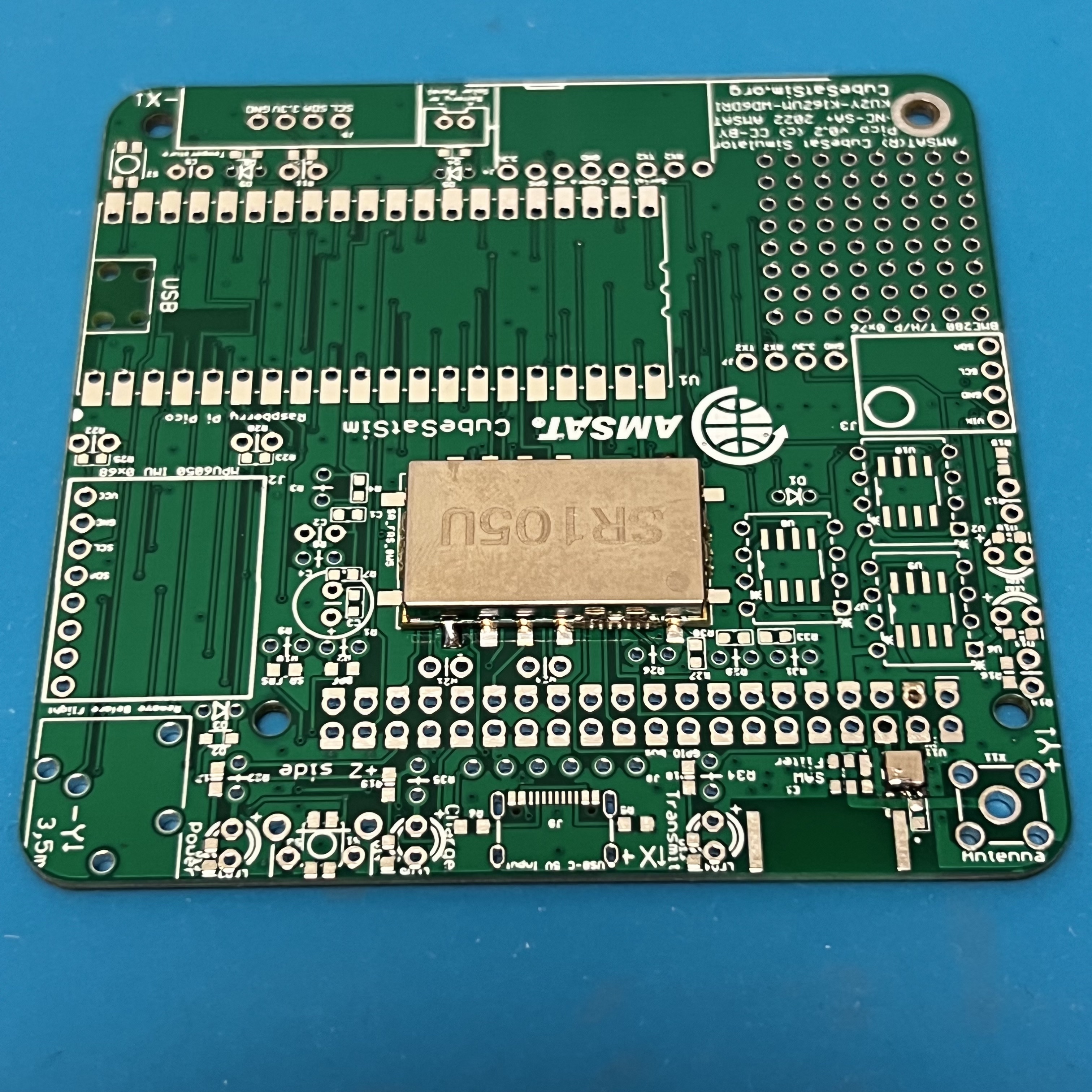
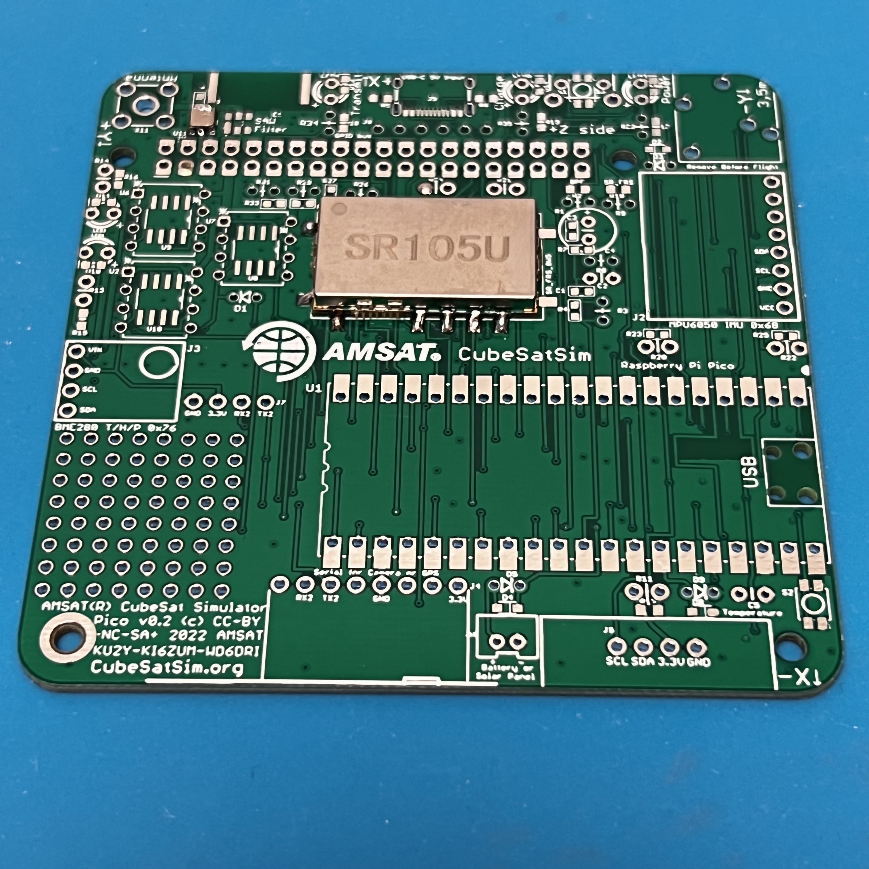
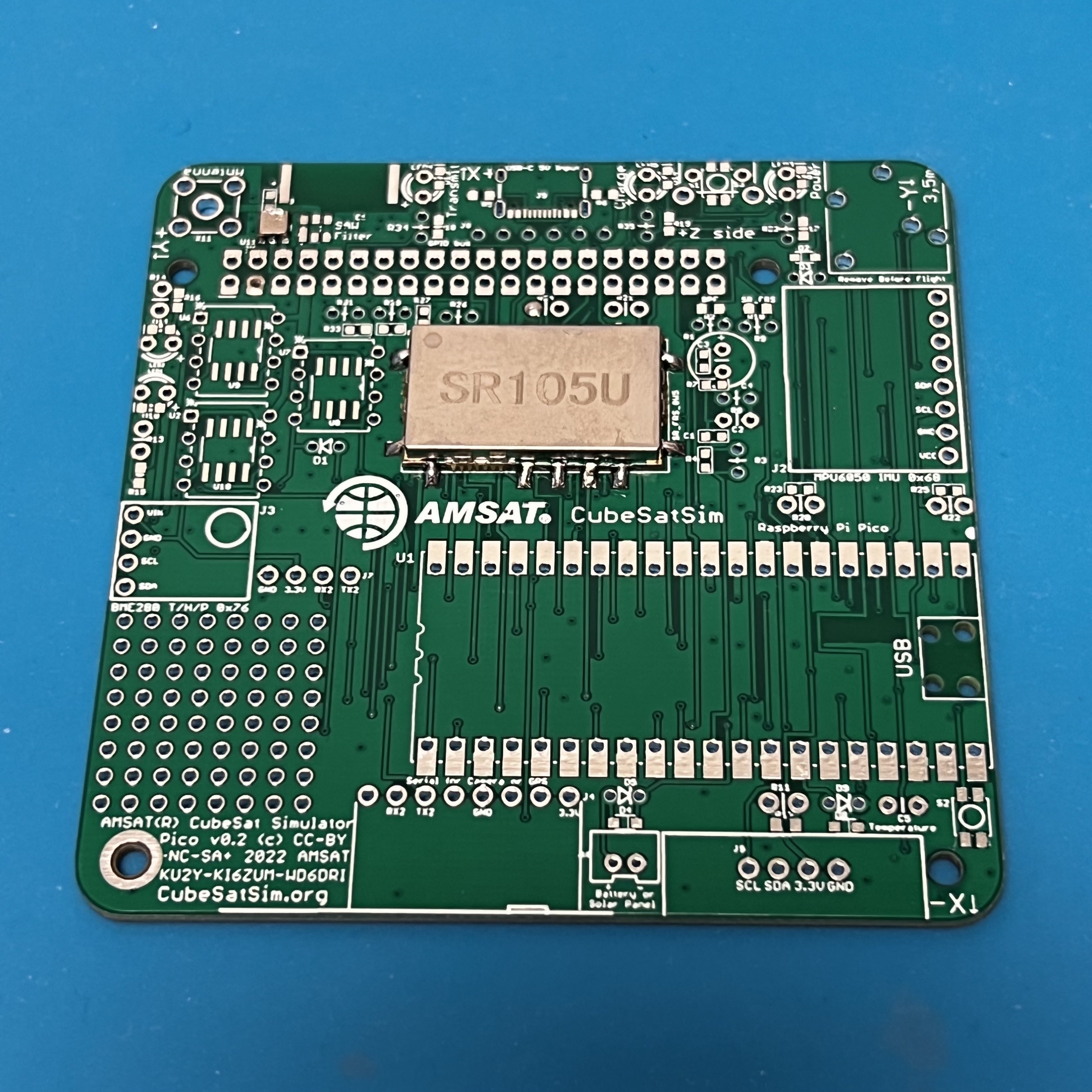
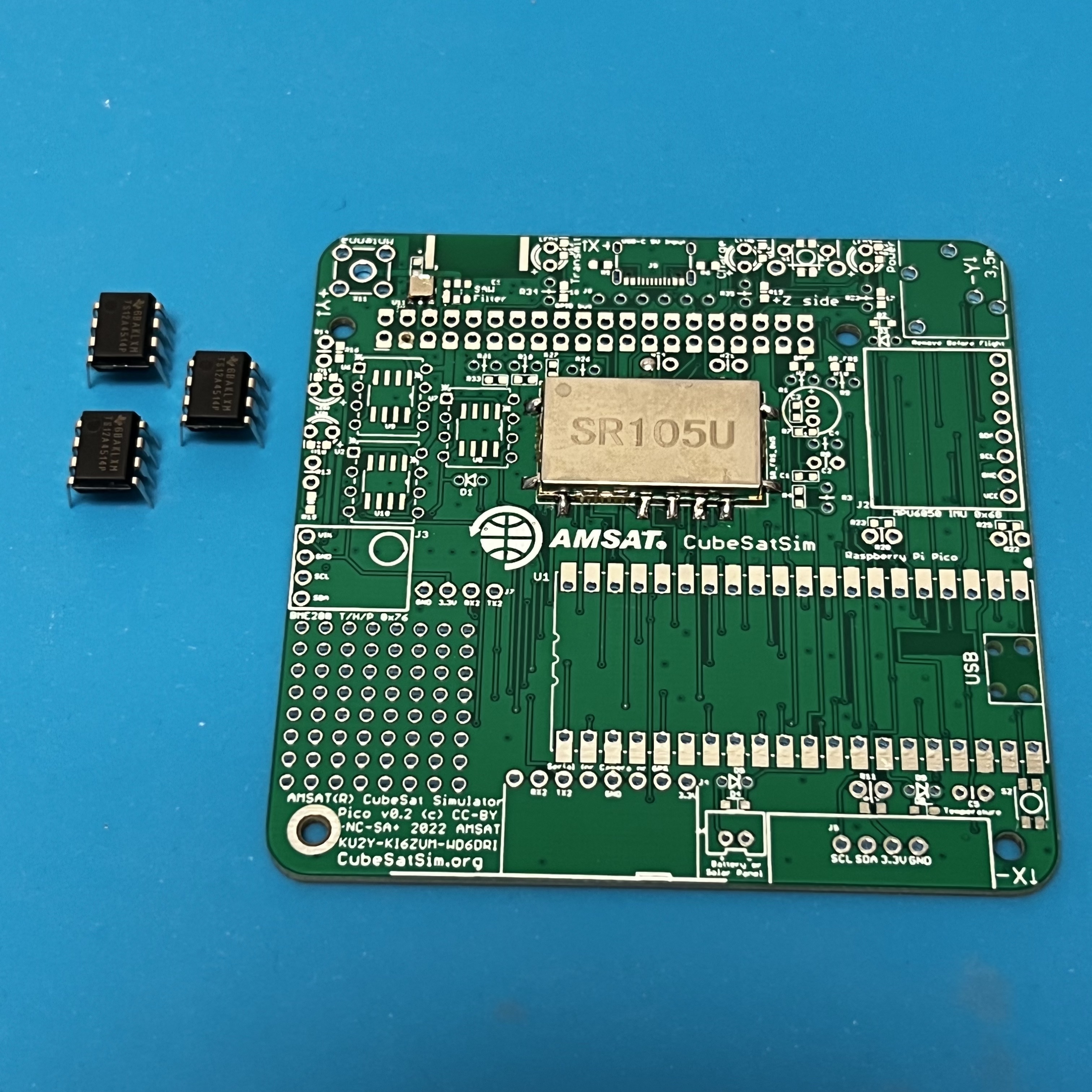
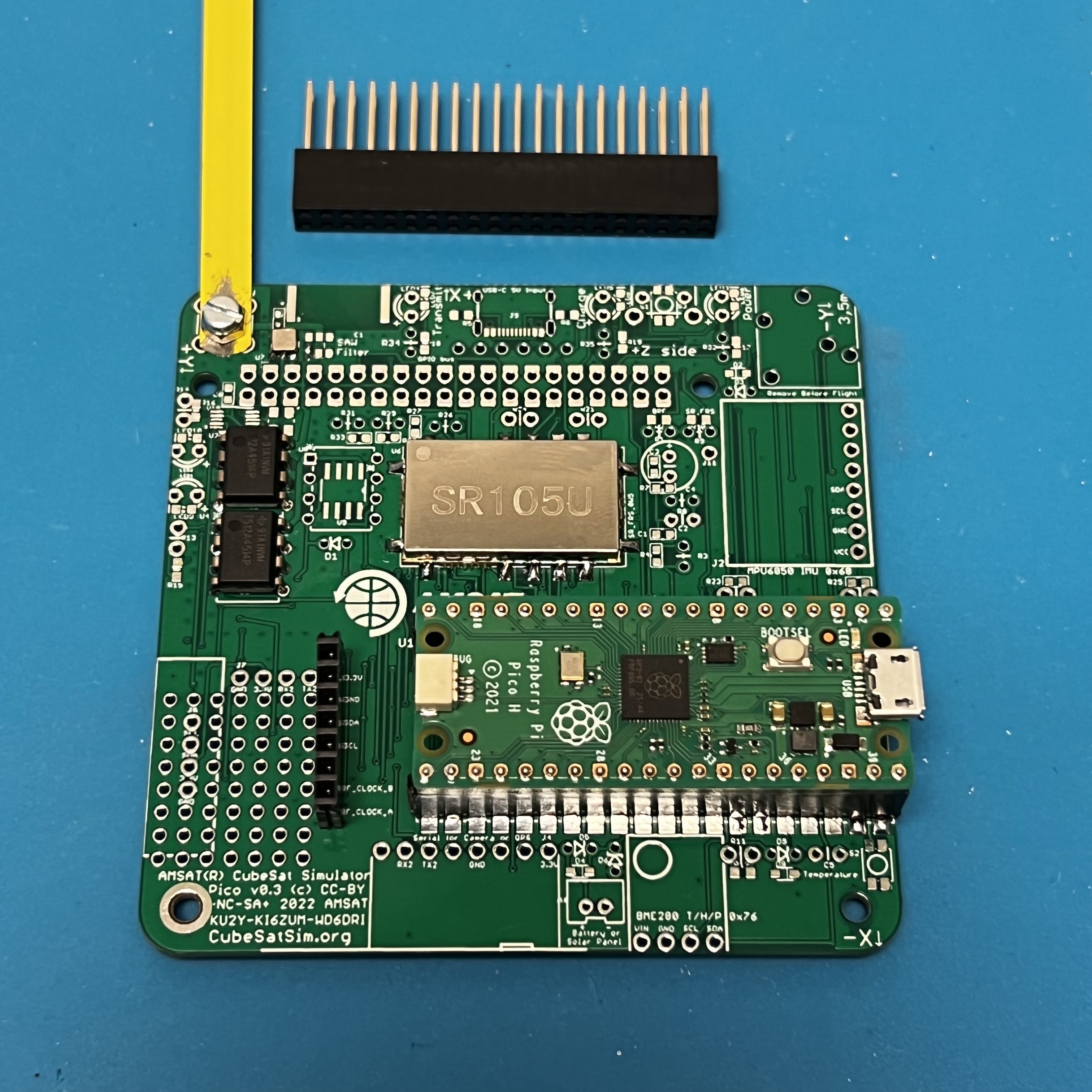
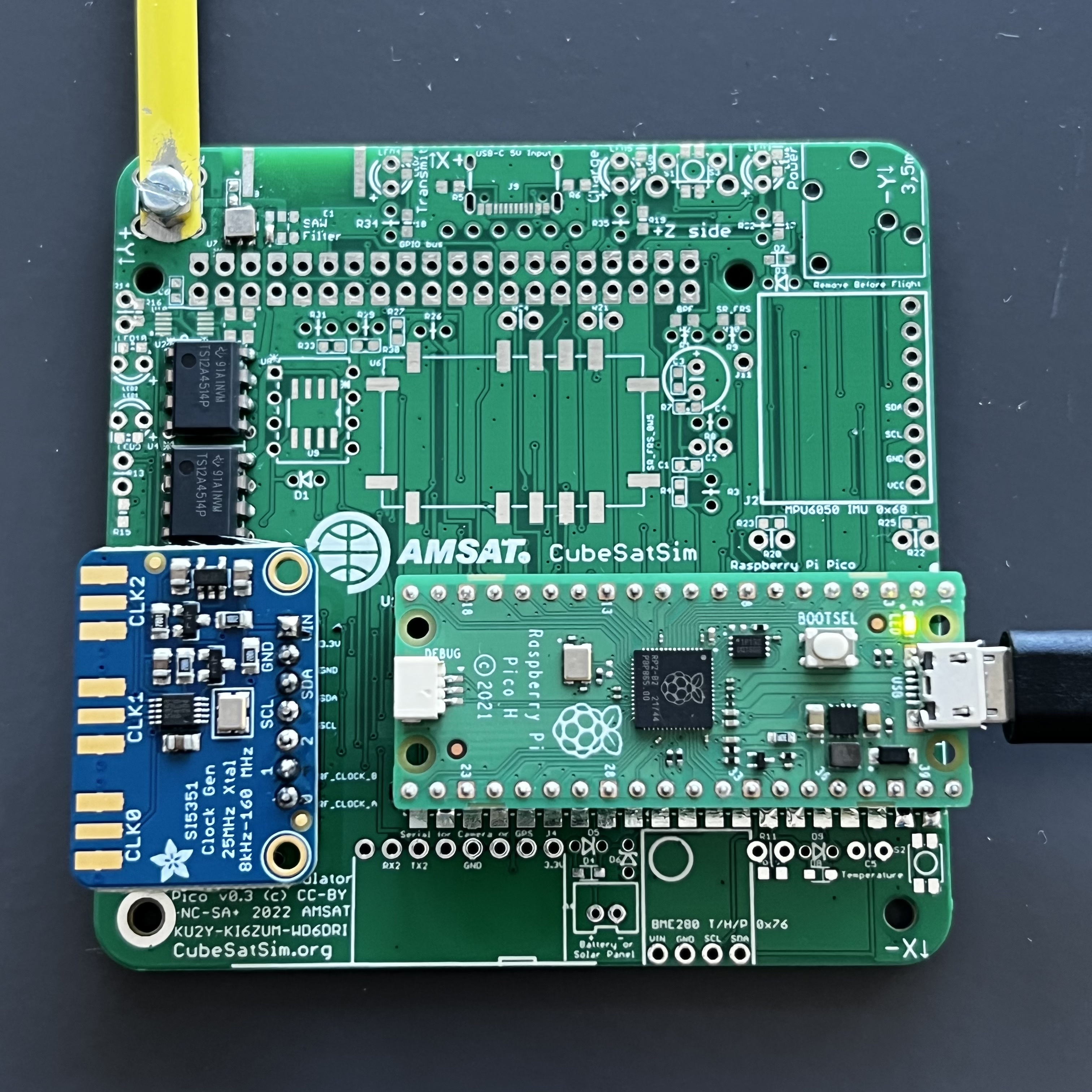
Here is the Pico v0.4 PCB:


Many of the photos here show the v0.3 PCB which is almost identical.
Here is the schematic:
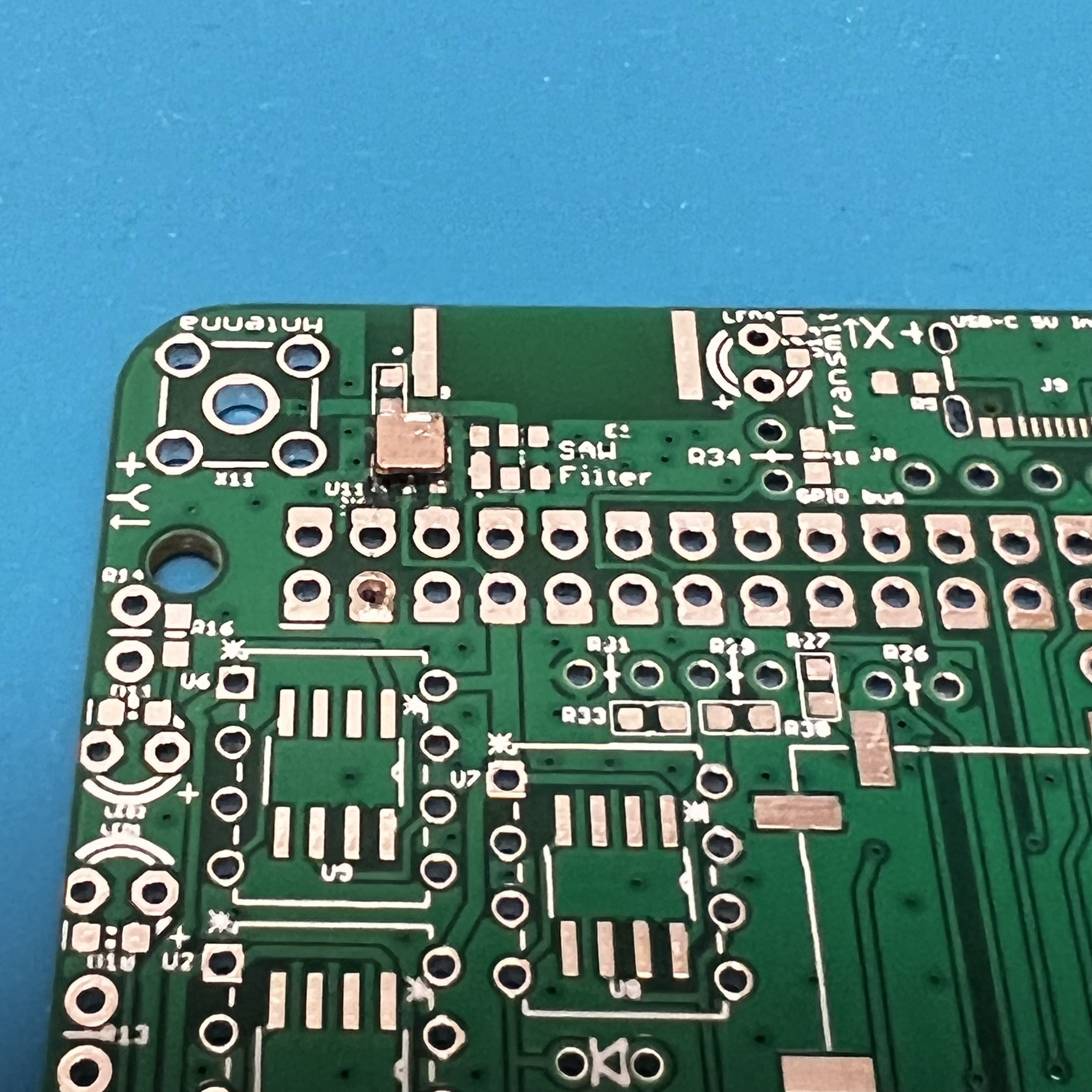
First solder the surface mount parts. If the SAW filter, SR_FRS transmitter, USB-C, and clockgen components are already mounted, you can skip to the Through Hole Parts section.

SMD Parts
To do the SMD soldering, you will need these tools:
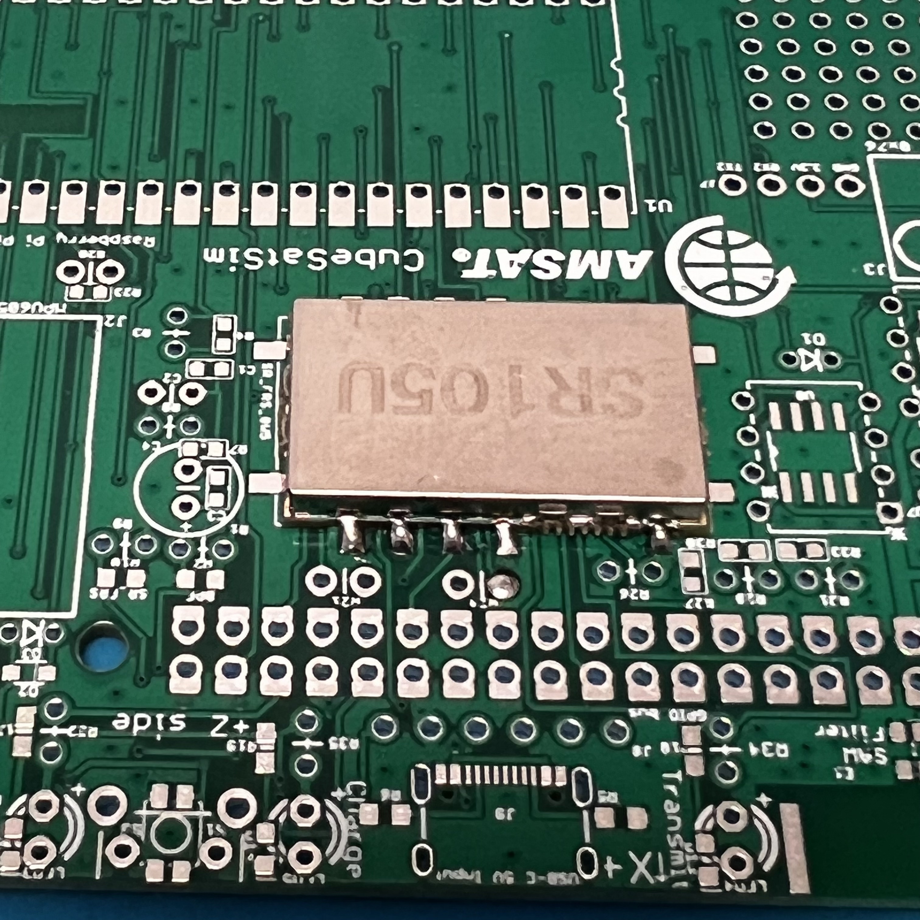
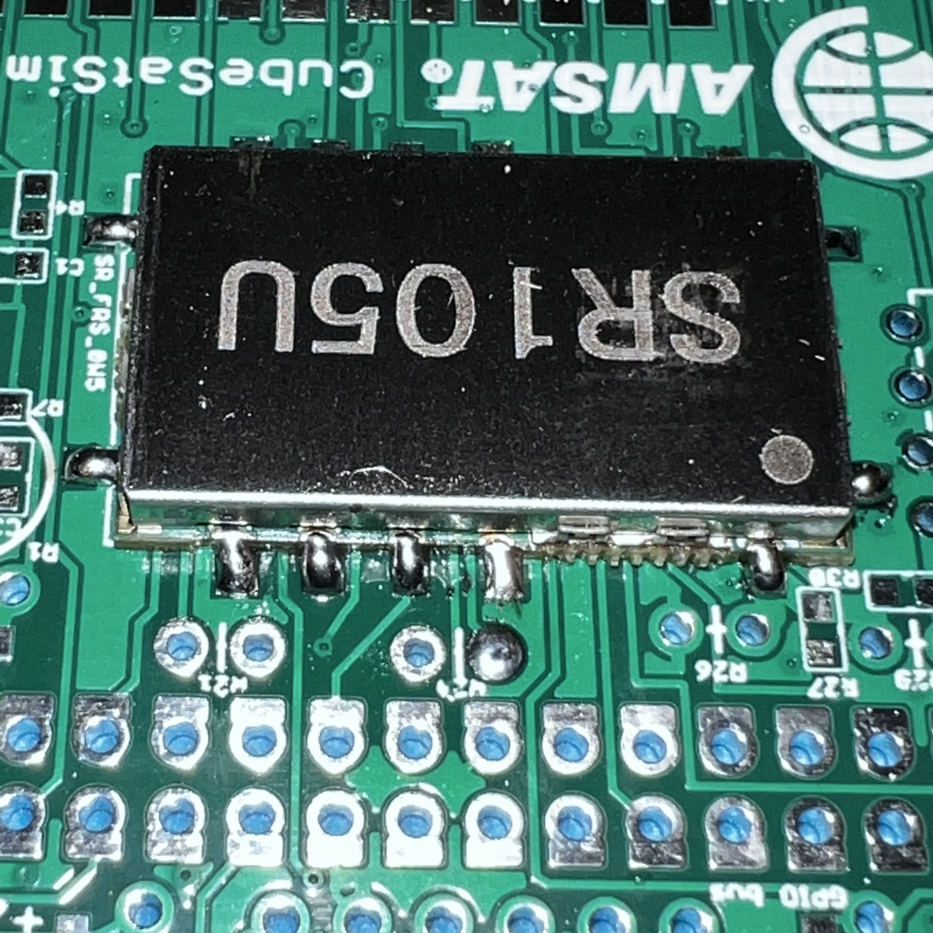
Start with the SAW Filter U7 and the SR_FRS board U6.
Apply liquid flux to the footprint,
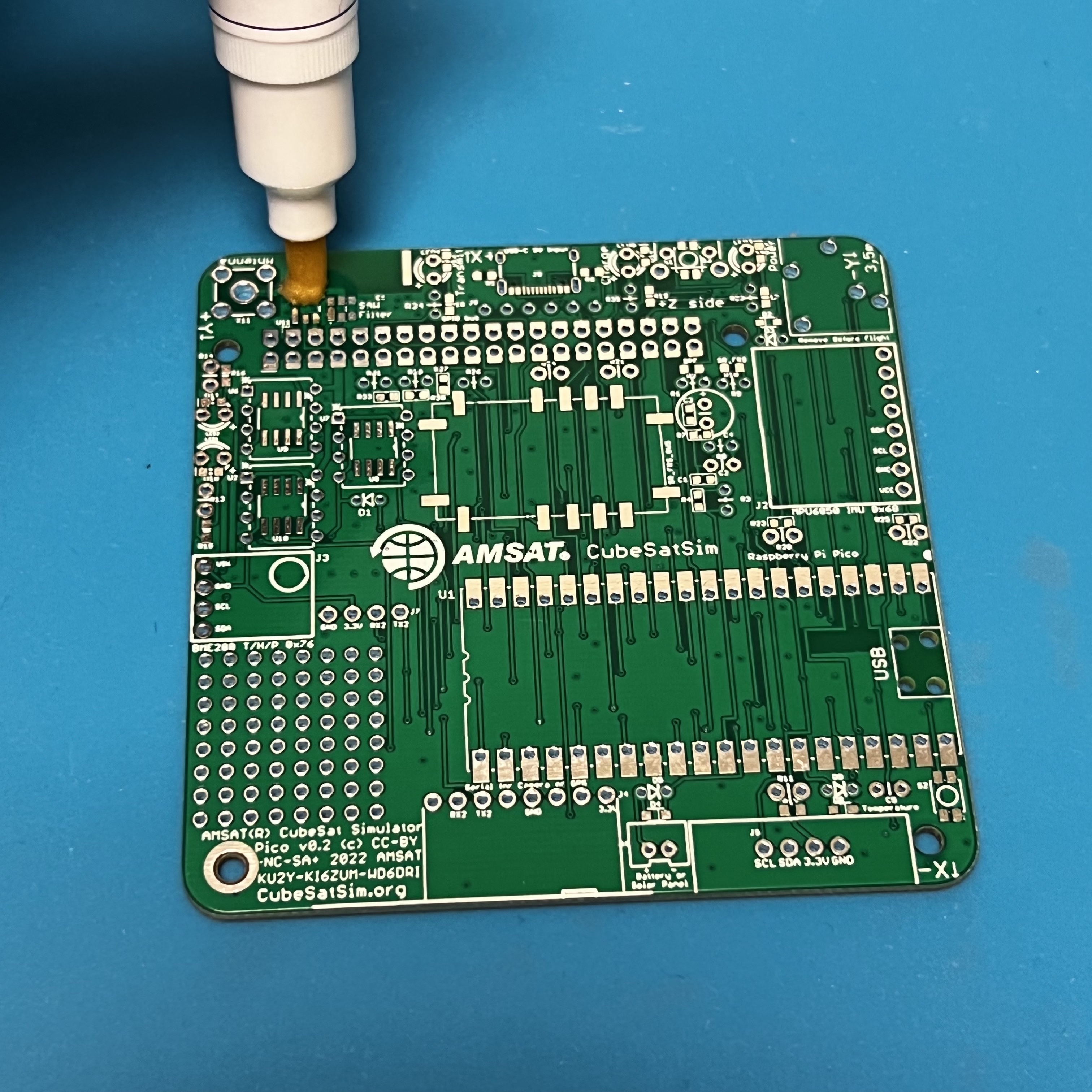
then place the SAW filter with tweezers.
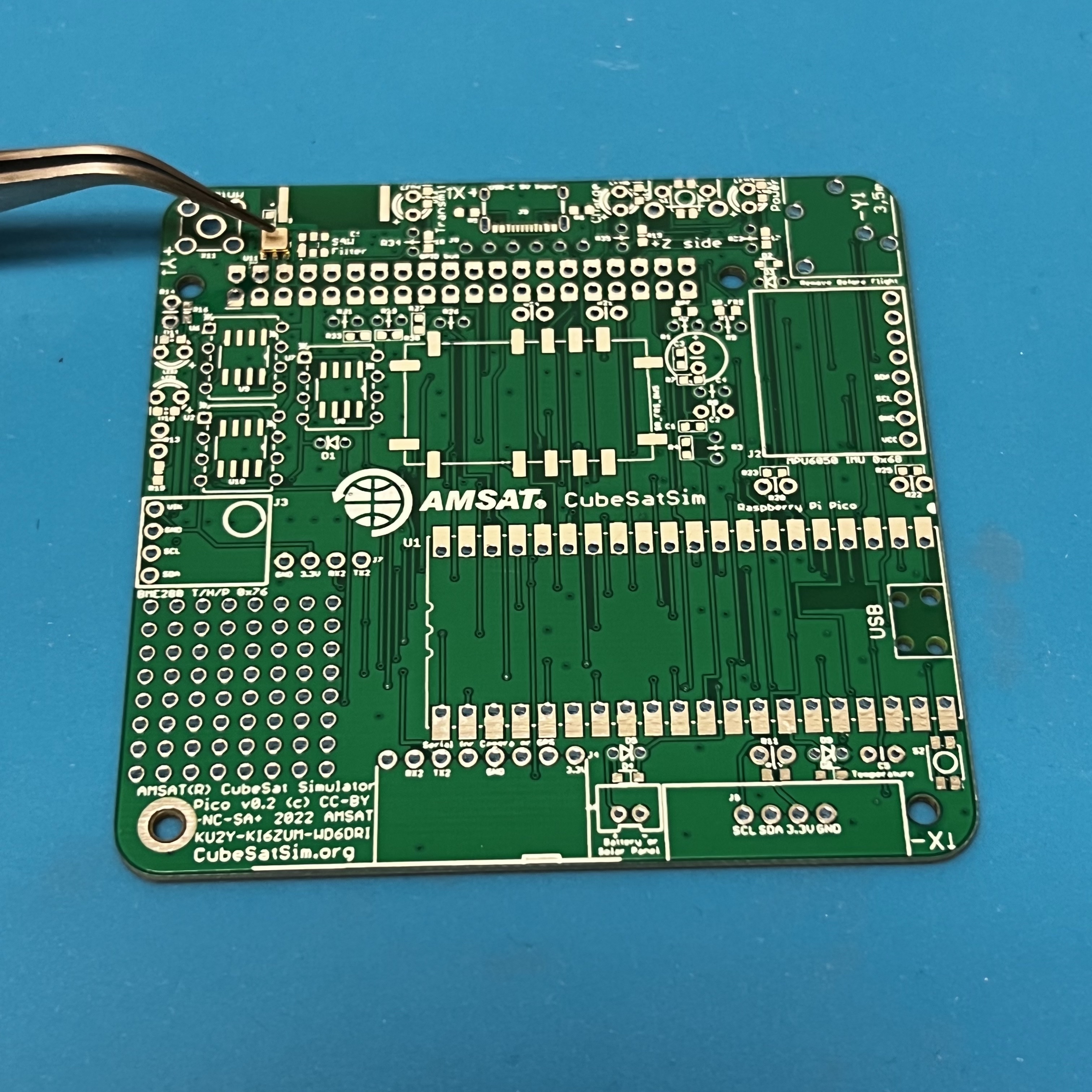
While soldering the first pin, hold the part in place by pressing down with the tweezers. Once one pin is soldered, the part should stay in place as you solder the remaining parts. Be careful not to apply too much solder. If there are any bridges, apply lots of liquid flux then drag the soldering iron across the pins and the bridge should go away.
Next solder the SR_FRS board.
Apply plenty of liquid flux to all pins, then place the part on the pads. Again, solder one pin while holding down the part with the tweezers. Here, I solder the pin on the lower left.
Then, solder one pin on the other side of the part, in this case the lower left pin. You may need to apply more liquid flux. Keep applying soldering until the whole pad is filled and the solder is a nice triangle that bridges the pin and the pad.
Continue soldering the rest of the pins.
This image shows a good solder joint on the right and a bad one on the left. On the right see the triangular shape that covers the pad and connects to the pin. On the left, the solder is in a ball and does not make good contact with the pin. Apply lots of liquid flux and reheat, making sure the pin gets heat.
Now, both pins are fixed.
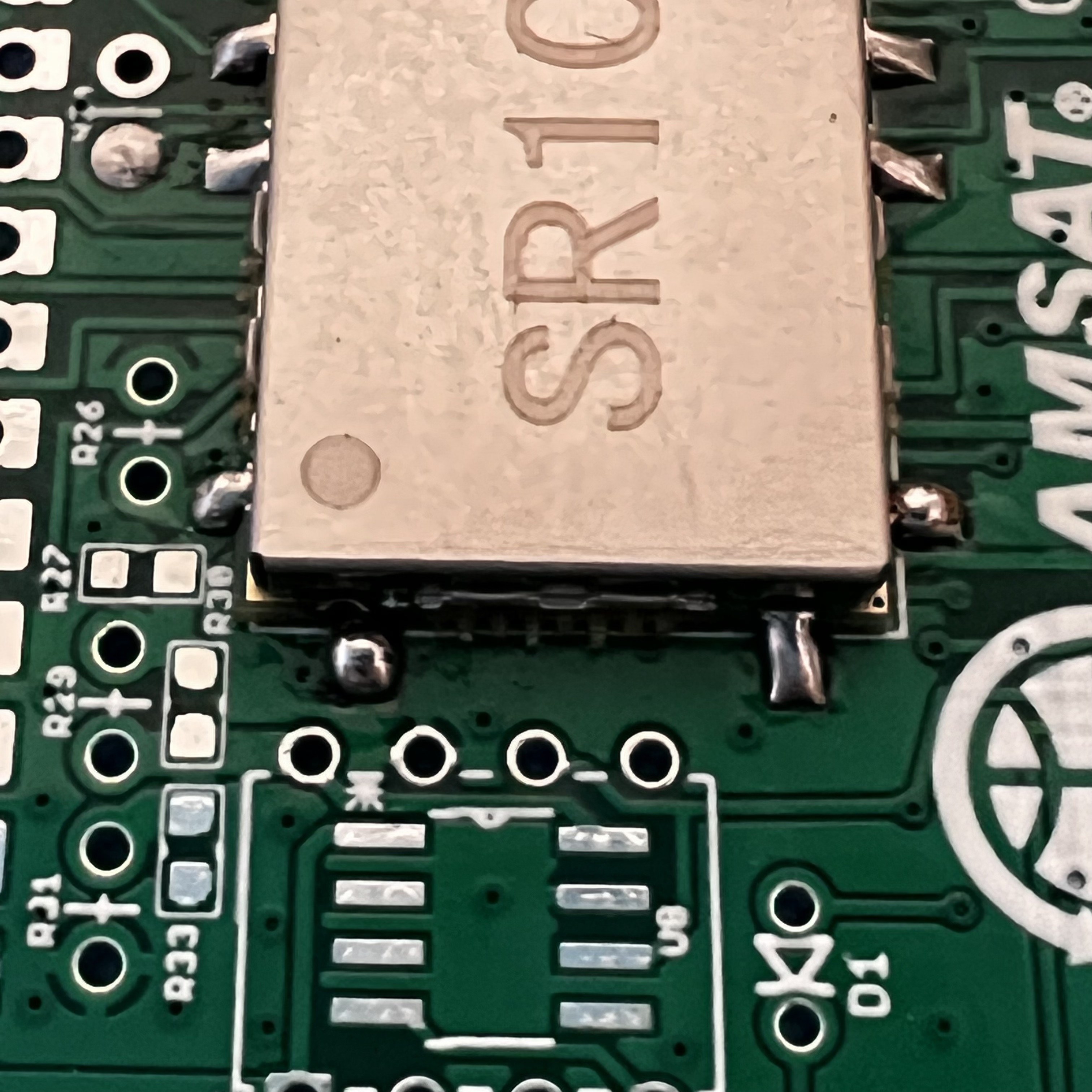
A closeup.
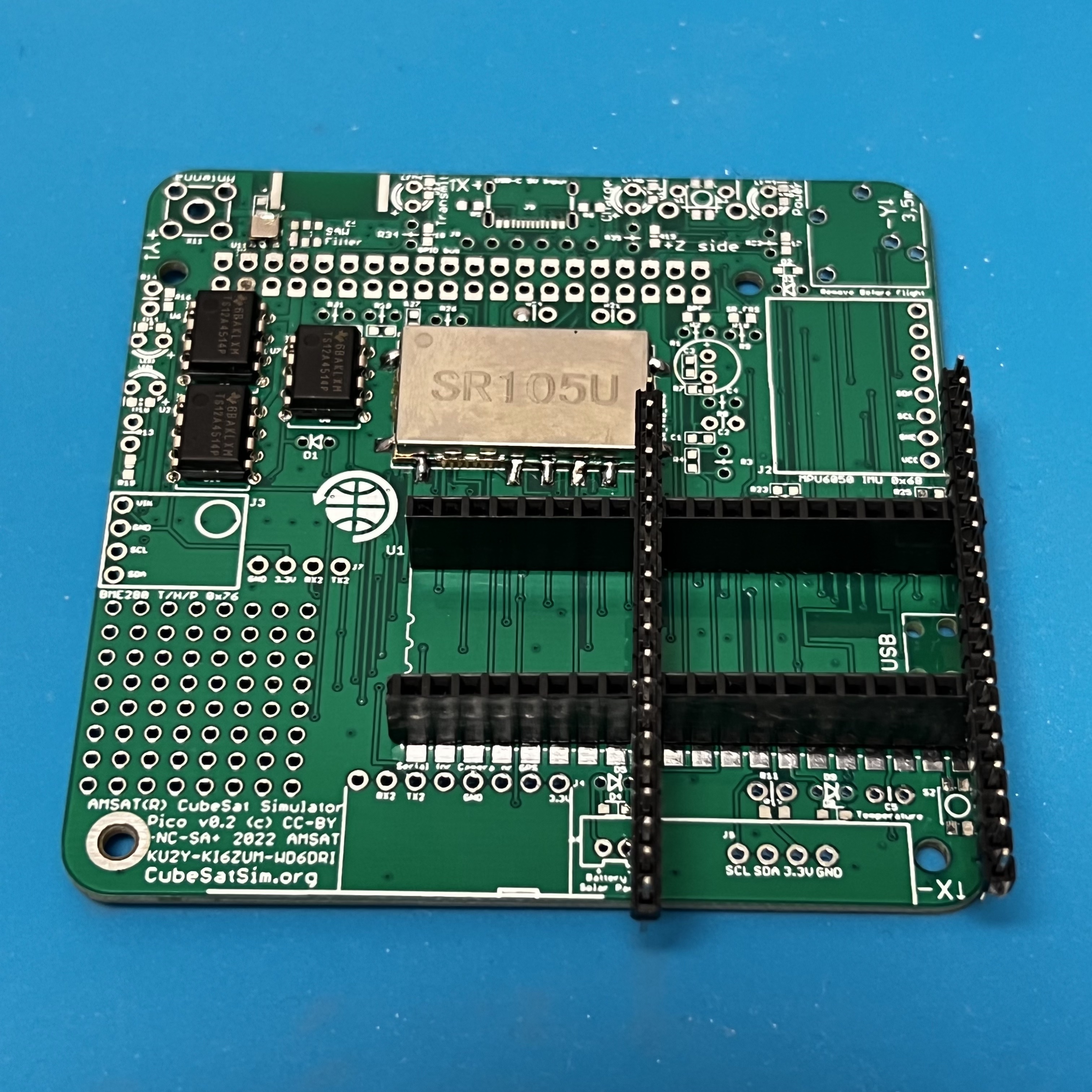
Finally, solder the SMD components USB-C connector J9, clockgen IC U10, crystal Y1, and capacitor C6 (no photo shown).
Through Hole Parts
Next, solder the three integrated circuits (IC) U2, U4, and U8:
You will need to bend the pins slightly to insert them in the PCB. Pay attention to the "dot" on the IC that marks pin 1, and make sure it is in the upper left when the board is in this position.
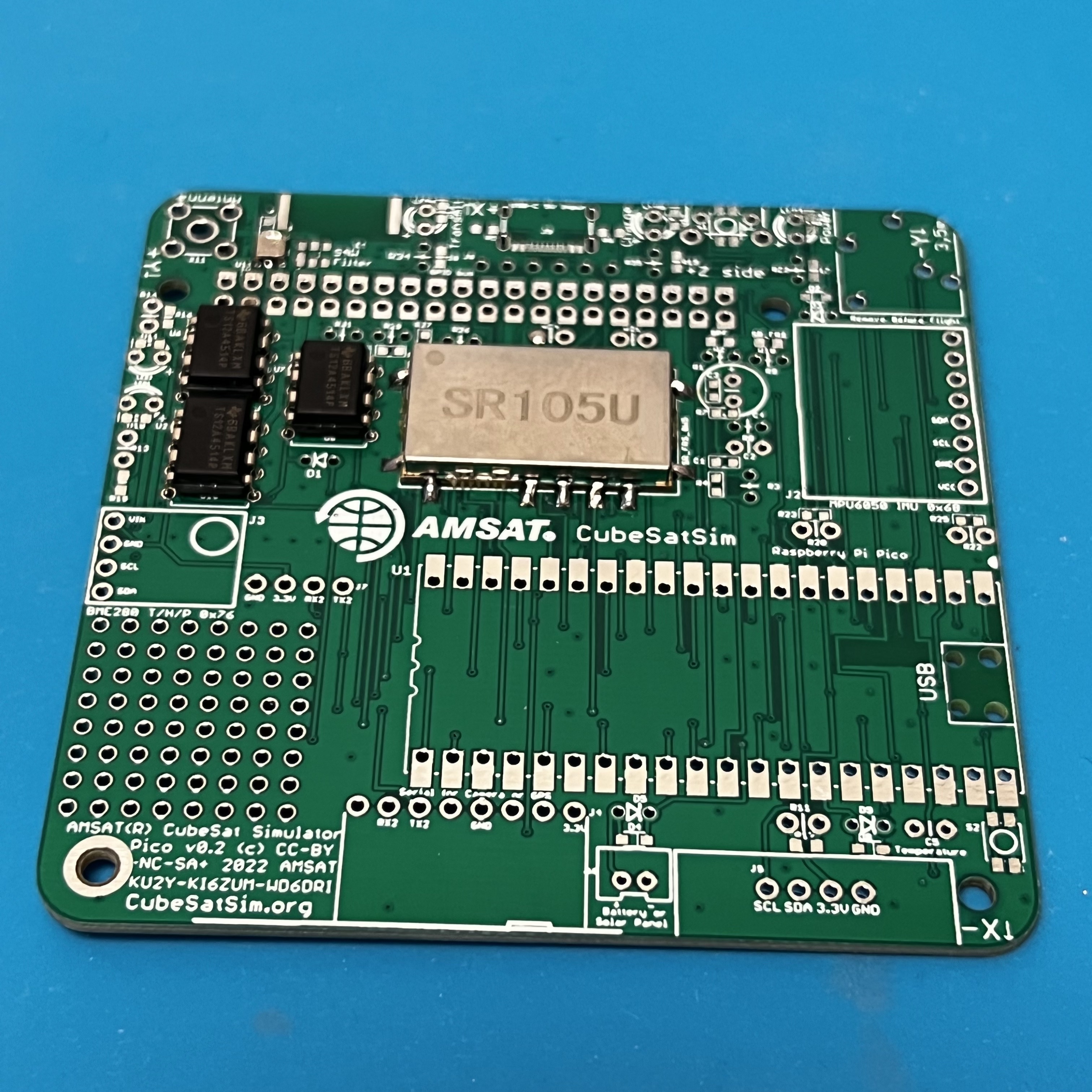
Solder only one pin on each IC, then double check the pin 1 mark and the IC is inserted correctly before soldering the rest of the pins.
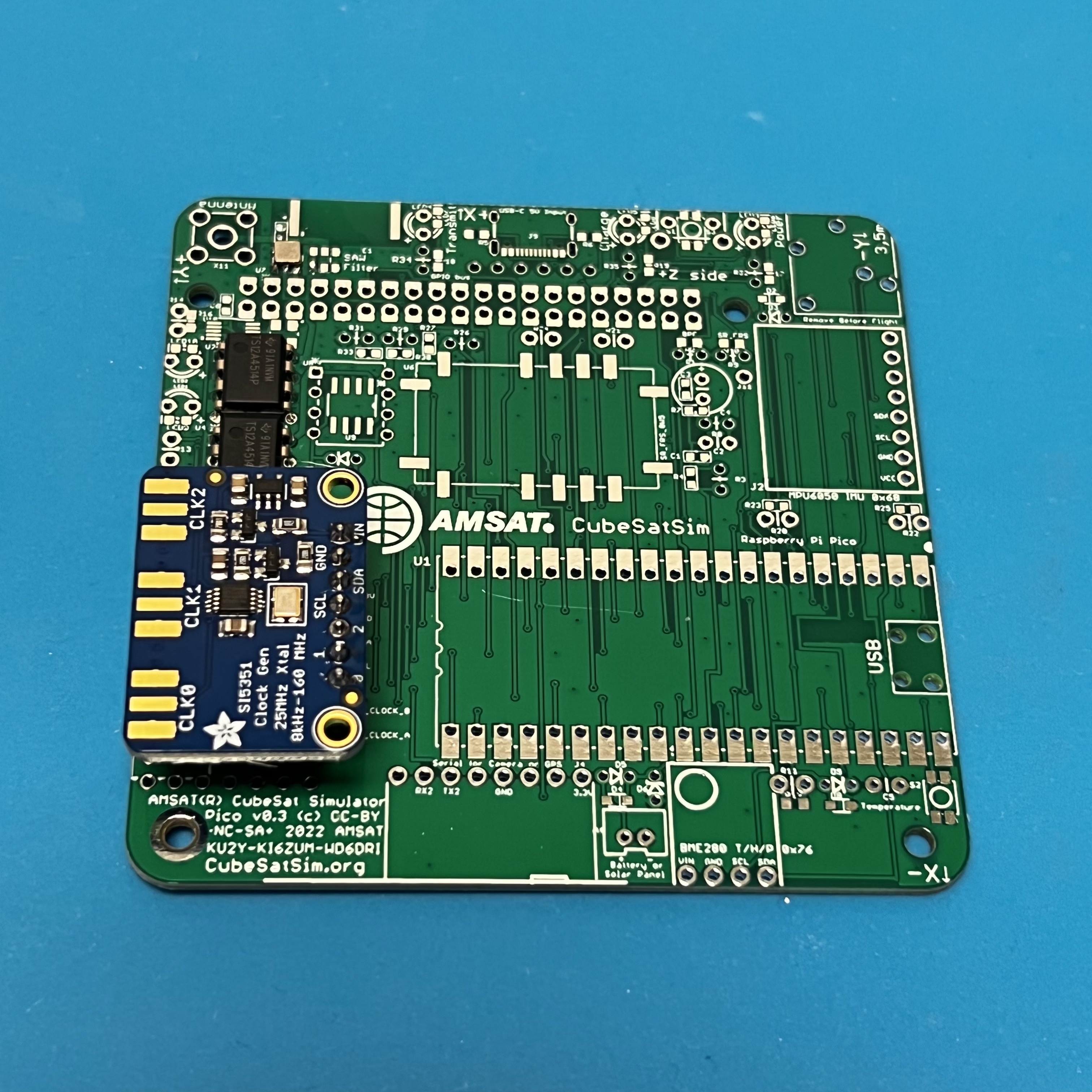
Now, if the Si5351 clockgen IC U10 SMD component is not installed, solder the Adafruit Si5351 breakout board using a female socket J6:
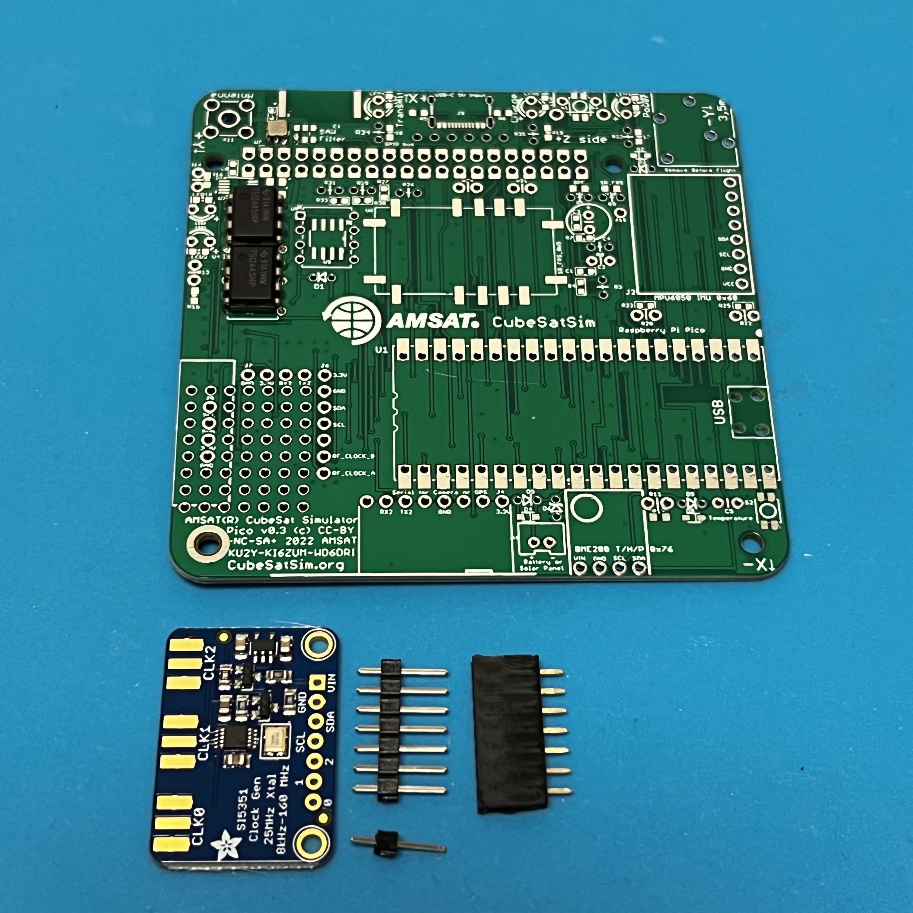
Solder the 1x7 pin female socket, the insert the 1x7 male pin header and solder onto the Si5351 board
Next, mount the 1x20 female sockets for the Pico U1. NOTE: You can also solder the Pico directly onto the board if you are comfortable drag soldering SMD parts.
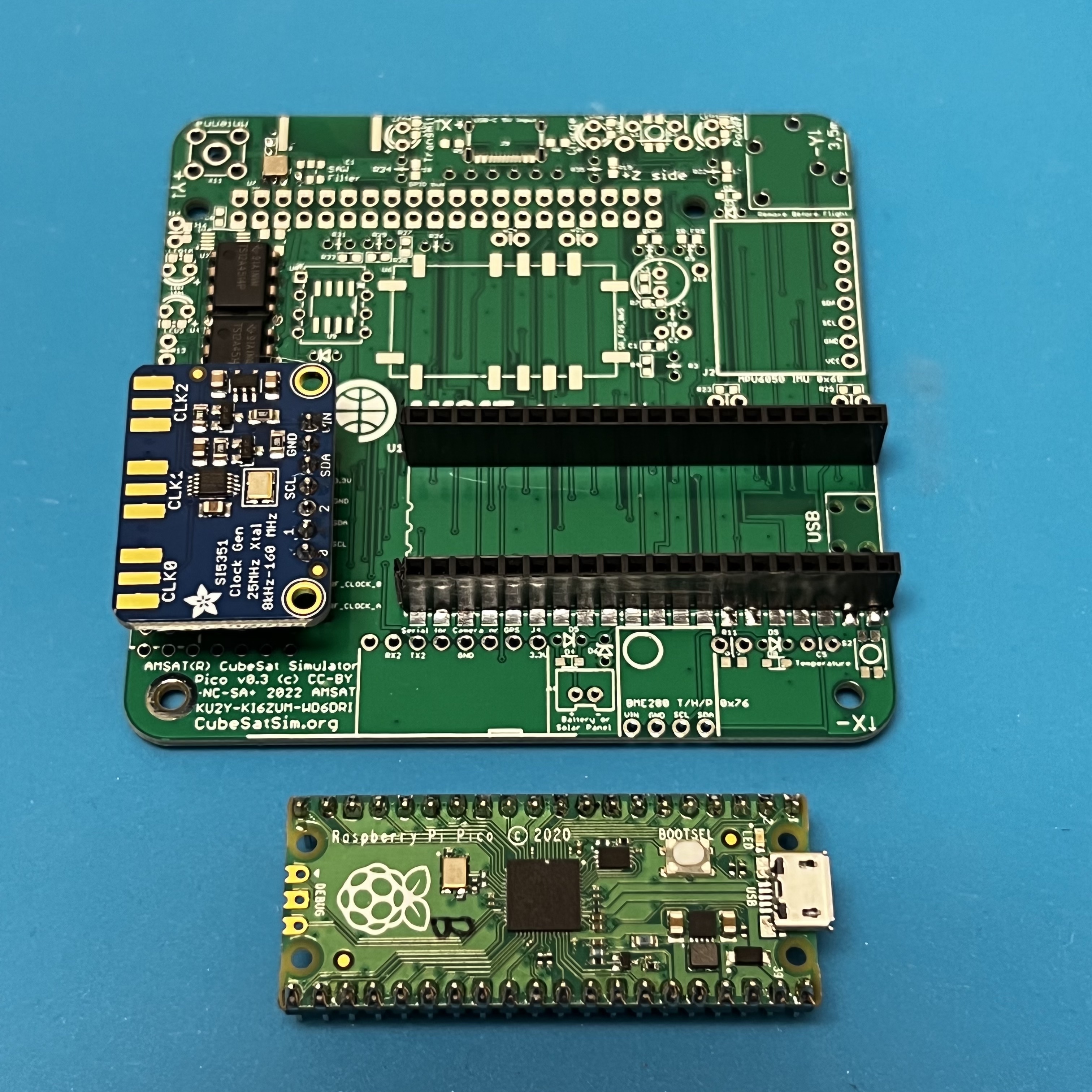
You can use the male pin headers to space and align the sockets for the Pico. Or, if you have a Pico with the male headers already soldered in (Pico H), you can plug in the Pico to set the socket spacing and alignment while you solder the first pins. Solder one pin on each side of the socket, then check alignment before soldering the remaining pins.
For the antenna, either mount the
- SMA connector, X11 (not shown)
- The chip antenna, E1, and a 0 Ohm jumper R28, (not shown)
- Or cut a length of tape measure to be 1/4 wavelength of 434.9 MHz (shown here)

Secure the tape measure antenna using the screw and the nut. The screw will cut threads as you turn it with pressure. Do not over tighten or the threads can get stripped.

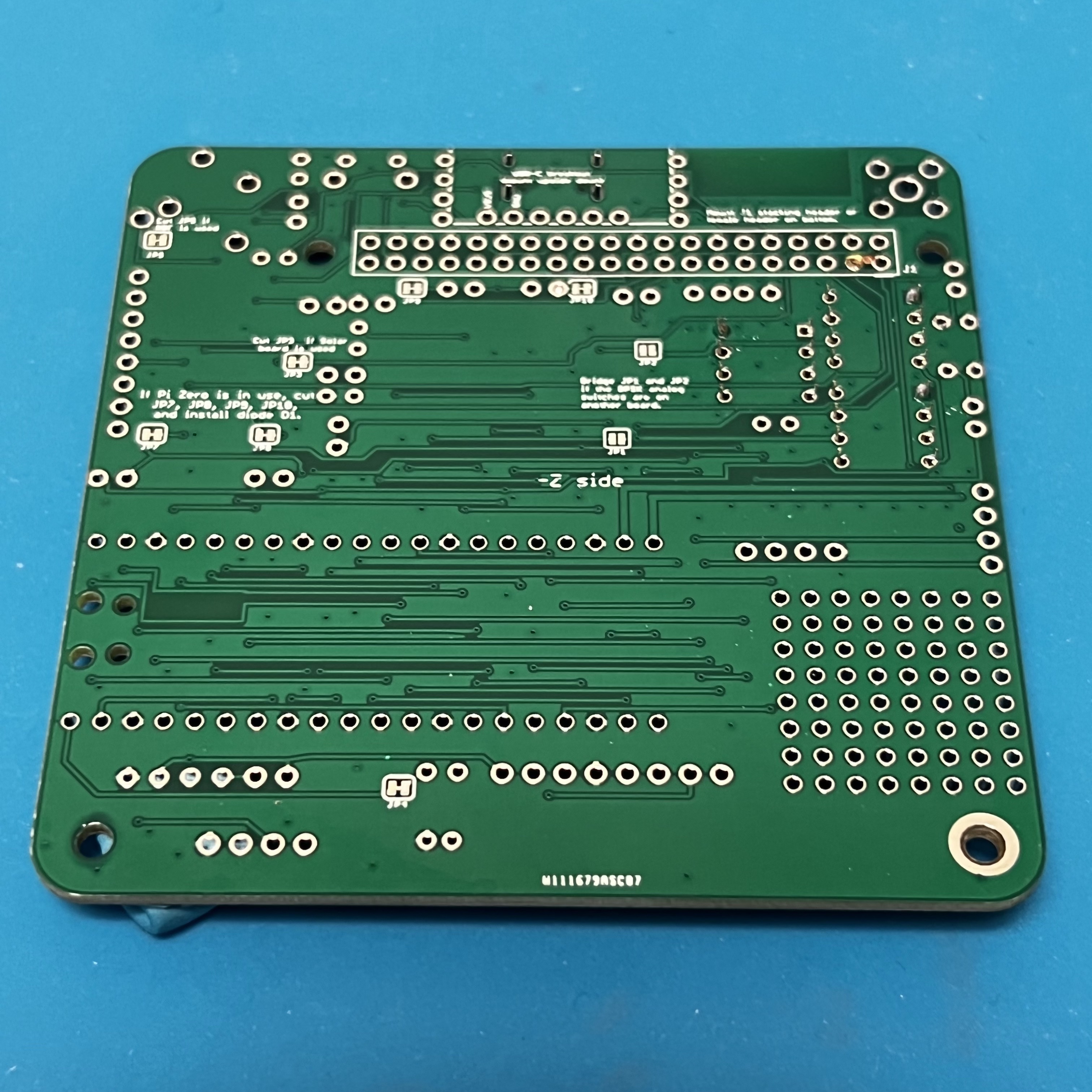
Next, install the stacking GPIO header J1:
It is inserted on the bottom as shown here:
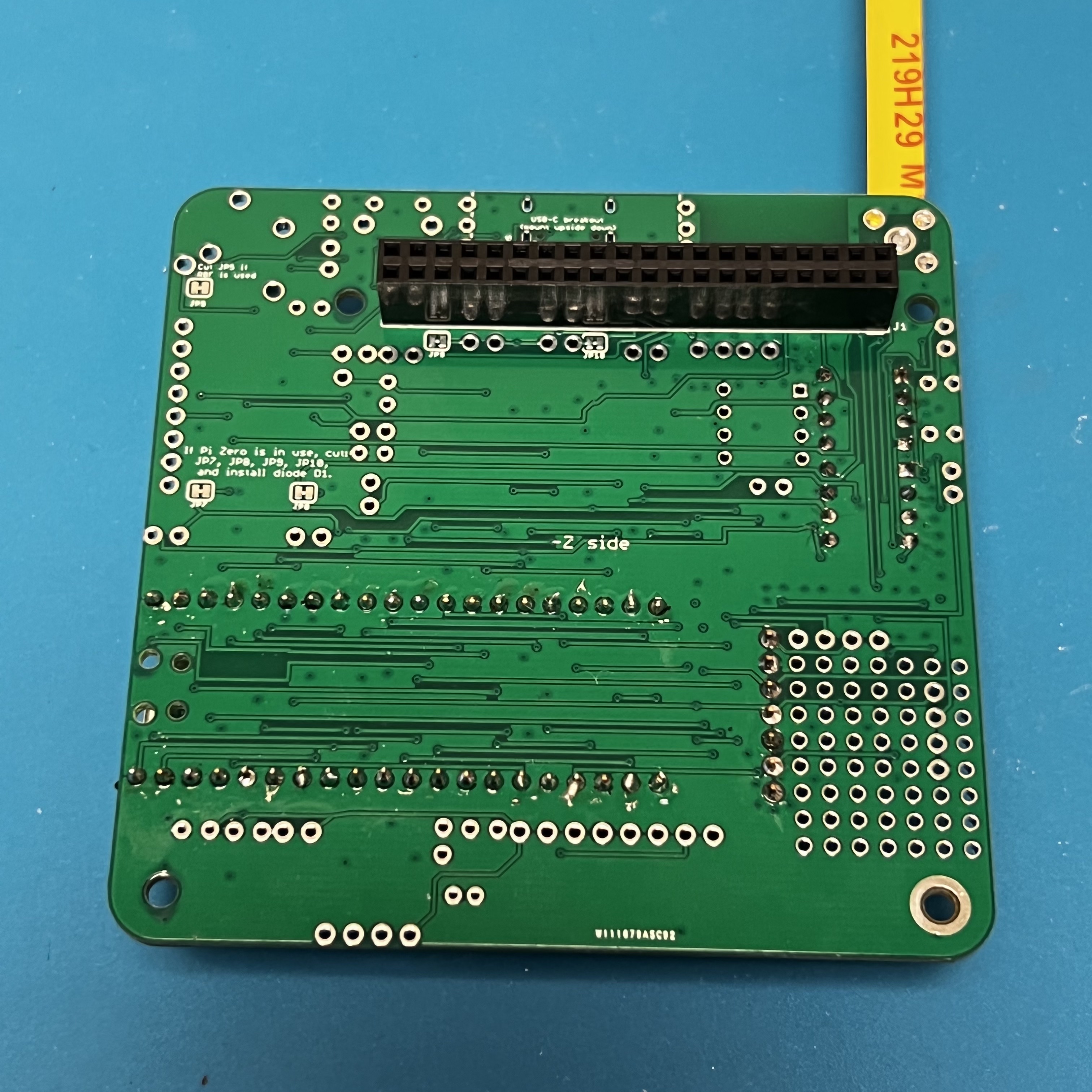
Flip the PCB over and solder all 40 pins on the top, being careful not to let the solder climb up the pin. Next, install the 68 Ohm 1/2 Watt resistors R26 and R31. These resistors are fatter and longer than the other resistors since they have to attenuate the transmitter power. Also install the 180 Ohm R29.
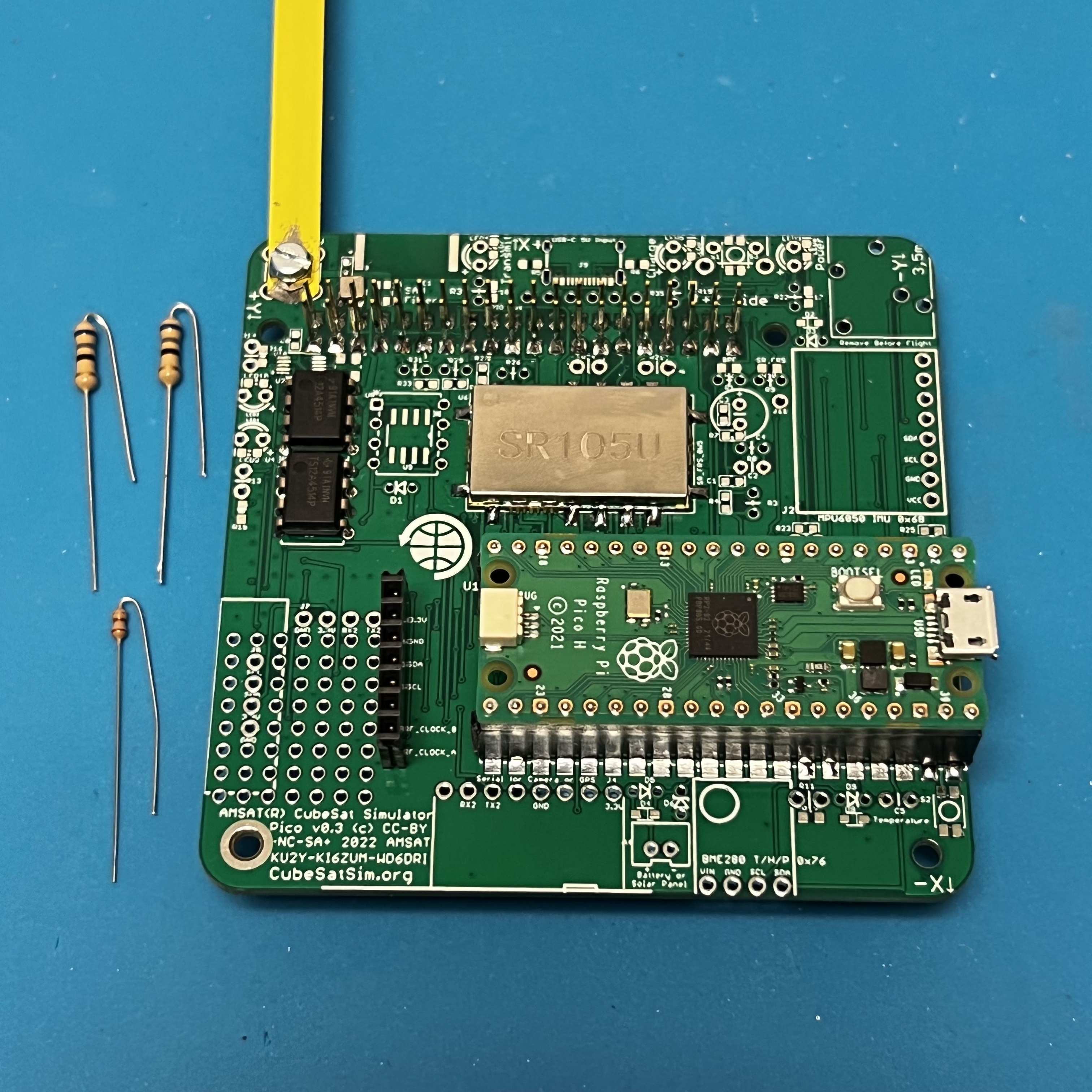
Here's how they look when they are installedL
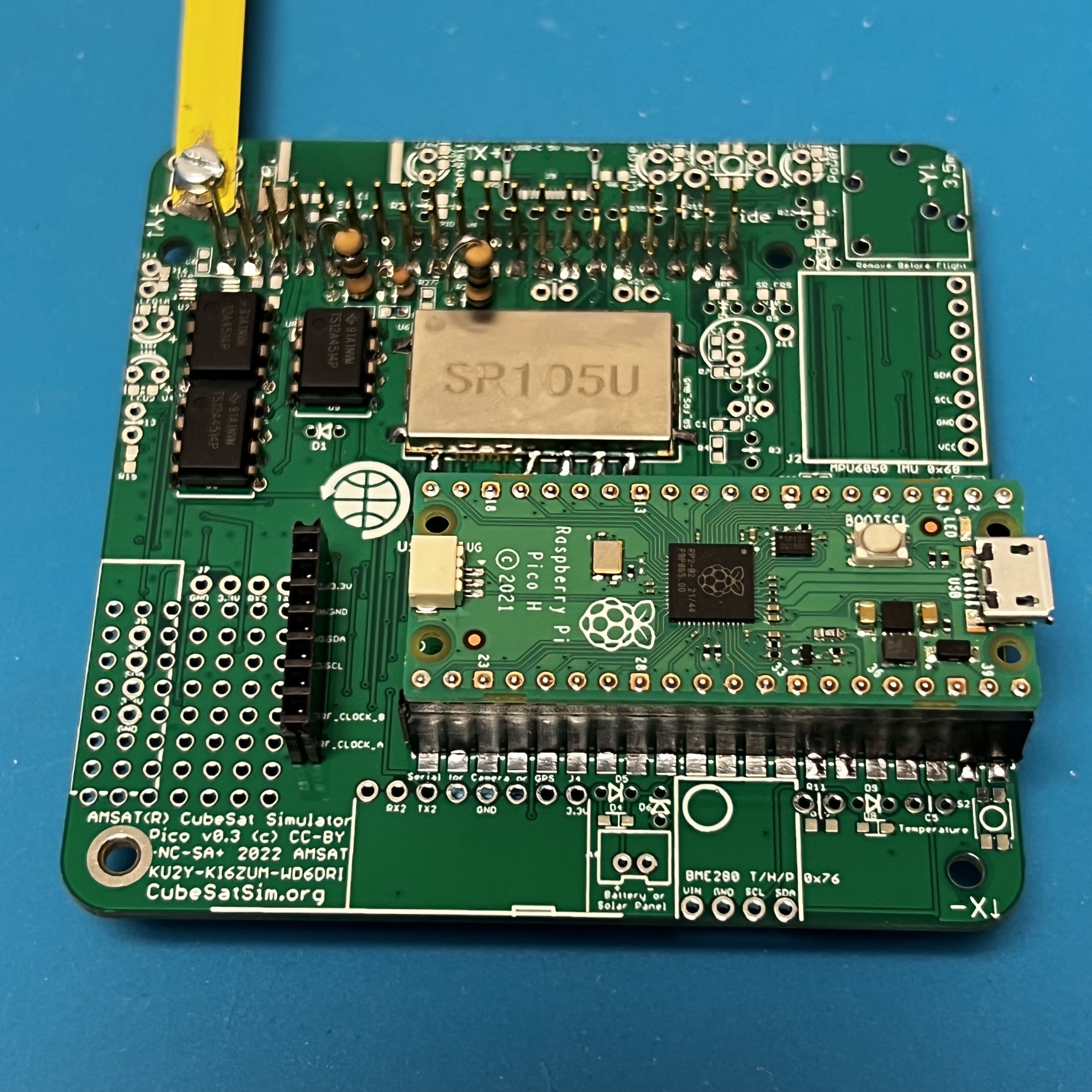
If the SMD resistors R2 and R10 are not installed, install the 1k resistors R1 and R9. If the SMD resistors R23 and R25 are not installed, install the 4.7k resistors R20 and R22.
(Not shown)
The CubeSatSim can now be tested in the FSK and BPSK modes. The Raspberry Pi Pico needs to be programmed first following these instructions:
- Download the latest .UF2 file here: https://github.com/alanbjohnston/CubeSatSim/releases
- Install it by following these steps:
- Plug your Raspberry Pi Pico into your computer using the micro USB port while holding down the BOOTSEL button (white button on the Pico). It should mount as a drive RPI-RP2.
- Drag the .UF2 file that you downloaded in step 1 to the Pico flash drive RPI-RP2.
- You can monitor the serial output using Arduino or a terminal emulator such as PUTTY to see the log files or make configuration changes.
You should receive a radio signal on 434.9 MHz. It will take a few seconds to power up. The built-in LED on the Pico will blink (unless you are using a Pico W which has WiFi - no LED will blink on this board) after a few seconds then stay on and blink off every 4 seconds or so. If you have a Ground Station with FoxTelem running, you can decode the packets. You can change modes by typing on the serial port (FSK is f while BPSK is b) or by pressing and holding the BOOTSEL button on the Pico (FSK is two blinks while BPSK is 3 blinks).
Install the Red, Green, and Blue LEDs LED3, LED4, and LED5, and the associated resistors R32, R34, and R35 (Not shown).
Solder the switch S1 and the RBF switch X1 (Not shown).
Next if the USB-C connector J9 isn't already installed, install the Sparkfun USB-C breakout board, J8, using a 1x6 pin header.

It is installed on the bottom of the PCB, but it is installed UPSIDE DOWN. Also, note that the solder mask covers the holes on the top of the PCB making the soldering a bit tricky. I'd recommend applying liquid solder and using a very small amount of solder to ensure that a good electrical contact is made.

Here's how it looks:

Install the capacitors C2 and C4 and resistors R3 and R8:
(Not shown)
Now you can test in the APRS, SSTV, and CW modes. On startup and when changing modes, the built-in LED on the Pico and the blue LED will blink when the CW ID is transmitted and you should hear it at 434.9 MHz FM.
Next, install the STEM green and blue LEDs LED1 and LED2 and the associated resistors R13 and R14.
(Not shown)
Install the two diodes D3 and D7, being careful about the polarity. With D3 in place, the Pico board can be powered through the USB-C connector and the battery board charged; the red LED will illuminate. With D7 in place, the micro USB connector on the Pico can be used to charge the Battery board as well.
(Not shown)
Install the diode D9 and 10k resistor R11 and capacitor C5. Install the right angle female socket J4 on the BOTTOM of the PCB.
(Not shown).
Batt Board v0.1
Here is the Batt PCB v0.1:
And the schematic:
The battery board components are:
- Batt PCB v0.1
- Stacking GPIO header
- 4 cell battery holder
- mounting square
- 4 NiMH AA batteries
- zip tie
IMPORTANT NOTE: There is a JST 2.0 connector on the board but the new design supplies power through GPIO pin 4 so this connector is only needed for other uses.
IMPORTANT NOTE: If the RBF switch is not installed (or JP5 not cut) or the RBF pin not inserted, the Pico will power up when the Batt board is plugged into the GPIO header stack.

Flip the PCB over to the bottom side and install the GPIO stacking header:

Flip the PCB over the top side and carefully solder the GPIO pins:

Stick the mounting square on the PCB ready to mount the battery holder:

Mount the battery holder on the PCB top then flip the PCB upside down and solder the two pins:

Trim the leads after soldering:

Insert the 4 NiMH AA batteries:

Check for a voltage around 5V with a multi meter set to DC voltage using the BAT+ and BAT- terminals on the top of the PCB:

Secure the batteries with the zip tie:

Trim the zip tie end:

Solar PCB v0.2
Here is the Solar PCB v0.2:


Here is the schematic:
cubesatsim-solar-0.2_schematic.pdf
The diodes D1 - D6 and resistors R3 and R4 are installed vertically:

Here is the polarity of the diodes:

They are installed on the PCB top then soldered on the PCB bottom:
Trim the leads after soldering:
On the bottom, install the 1x4 pin header

Use this pin header to test the INA219 boards before soldering and mounting them.
On the PCB bottom, install the GPIO header J1 and three 1x6 female sockets:. Alternatively, after testing the INA219 boards can be soldered directly without sockets.

Flip the PCB to the top and solder.

Install 3 INA219 boards on the bottom:

Here they are installed. Set the jumpers as marked on the PCB.

Install 12 JST 2.0 connectors on the top - there are two for each of the sides of the CubeSat. Apply a drop of superglue to the plastic before attaching them so they will hold together while plugging and unplugging cables:


DO NOT INSTALL a connector for the battery, as the power goes through the GPIO connector.
Install 4 female headers 1x6:

Install 4 INA219 boards on the top:

Here they are installed with the jumpers set per the markings on the PCB.
