Synthesizer Prototype - WCP52/docs GitHub Wiki
Git repository: WCP52/synthesizer
Our test-signal synthesizer uses the AD9958 dual Direct Digital Synthesis (DDS) synthesizer. In the first iteration of the design, we are building a standalone synthesizer board to hold only this part, allowing us to experiment with the circuit in isolation.
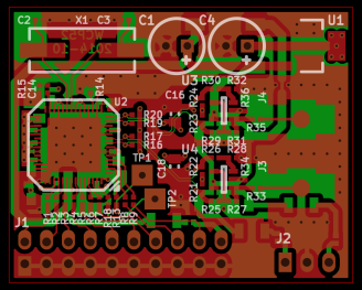
Layer renders: top, inner2, inner3, bottom
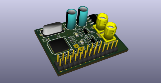
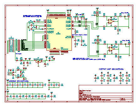
This board provides basic interfacing to the AD9958 dual DDS chip. All digital control signals, with the exception of the modulation control pins (P0..P3, pins 40..43), were connected to a header through 100-ohm series termination / protection resistors. P0..P3 were left fixed due to lack of layout space and the fact that we have no need for them in the prototype.
*In the final build, we plan to interface with the AD9958 through an optional CPLD, allowing end users to experiment with different configurations. Here, P0..P3 will be connected to the CPLD.
X1: This crystal provides the reference frequency for the DDS. We selected the 9C-25.000MEEJ-T from TXC, which provides ±10ppm frequency stability from -20°C to 70°C. The load capacitance is 18pF; we used two 15pF load capacitors to allow 3pF as a result of layout capacitance and pin capacitance.
The crystal was placed near the DDS, but as far away as practical from the analog outputs, to avoid coupling.
The AD9958 requires two rails, one at 3.3V and one at 1.8V, with a combined current draw at peak around 150mA. We elected to supply the board with one 3.3V supply, protected by a 250mA-IH current-limiting thermistor and a reverse-protection Schottky diode. A common 1117-type low dropout regulator provides the 1.8V rail, and a ferrite bead (600 ohms at 100 MHz) provides some isolation for the separate, 1.8V analog rail.
The output amplifiers are op-amps, which we are powering using a split +5V/-5V rail. This is provided separately, with 100mA-IH current-limiting thermistors.
The AD9958 has a tricky output stage; it is a differential current sink, which expects to be terminated into VDD, and whose output compliance range is 500mV above and below VDD. The intent, according to the datasheet, is to terminate into a center-tapped transformer, but this will restrict the frequency range. Instead, we connected the outputs to differential transmission lines (Z0 = 50, Zdiff = 100) which were referenced to VDD and parallel-terminated to VDD at both ends. This gave a satisfactory voltage range.
The AD9958 requires a resistor to set the full-scale output current. Higher currents give larger signals, lowering the requirement on gain-bandwidth product for the final output amplifier; the datasheet recommends not exceeding 10mA, as this will degrade the signal integrity. We elected to use the datasheet example, a 1.91k resistor which sets full-scale to almost exactly 10mA.
The output signal at this stage is still small, and needs to be shifted to near 0V. It is possible to use a capacitive DC block, but it would be complicated for the wide frequency range. The signal is still small enough to use inexpensive video op amps, so we chose the LMH6714 (400 MHz bandwidth at low amplitudes, $2.10 in low quantity) current-feedback amplifier for both channels. A differential amplifier was used to convert to single-ended, providing the necessary voltage shift; 360 ohms was selected as the feedback resistance by starting with the datasheet's suggestion and then tweaking the value for an ideal frequency response in simulation. The '50-ohm' termination resistors at that end were adjusted to 53.6 to compensate for the input impedance of this differential amplifier.
This amplifier directly drives 50-ohm SMA outputs.
A slightly better signal purity was achieved in simulation by adding a 2.2k resistor from the op-amps' outputs to the -5V rail. This offsets the positive bias from the 1.8V-terminated transmission line, presenting a symmetric load to the output.
Once PCBs and parts were delivered, and the synthesizer prototype was built, we tested the board. After some minor, ever so slightly horribly irritating issues involving misunderstanding the protocol, we got the synthesizer to output a waveform.
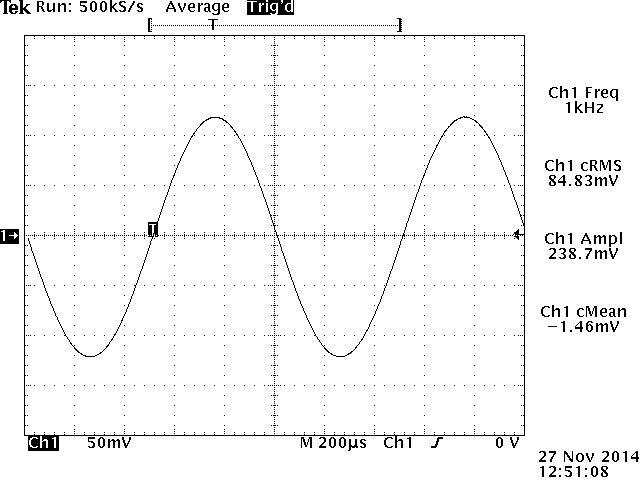
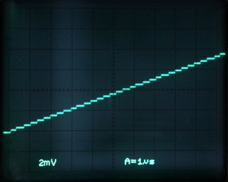
Here, for the sake of demonstration, is an image of the discrete steps generated by the DDS system to generate a 1 kHz waveform. These steps are very small (the device uses a 10-bit digital to analog converter, so the steps are 1/1024 of the total amplitude), so it helped to use an old, analog oscilloscope for its ability to show small waveform features reliably.
The synthesizer board amplifies the DDS output unfiltered, so sampling images above the Nyquist rate (250 MHz) are clearly visible. The waveforms will be filtered properly before the output amplifier. Here are Fourier transforms of the signals, generated using a 400 MHz digital oscilloscope (Tektronix TDS-380):
Once the output amplifier has been built, we will obtain and use a spectrum analyzer to fully characterize the output spectral purity.