Prototype PSU - WCP52/docs GitHub Wiki
Our system requires a number of power supply rails: +10V, +5V, +3.3V, -5V, and -10V. This is enough to be inconvenient to provide using bench power supplies, so we built a triple DC-DC converter board to provide them from +10V and -10V inputs.
All circuits were based on the self-oscillating buck converter design presented by Roman Black, which is simple, small, efficient, and could be easily built with the parts we had on hand.
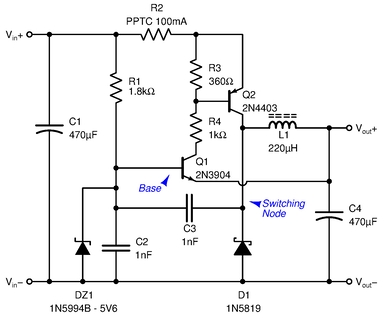
The +5V regulator was based on the original design, with two modifications: it was run at a higher frequency (we found the circuit worked well up to 200 kHz, allowing smaller parts to be used at a slight cost of efficiency), and a PPTC current limiting thermistor was added for short circuit protection. Here is the circuit diagram as we built it:
Here is an oscilloscope capture of the switching node (channel 1, labeled "Switching Node" on the schematic), which is filtered to give the output voltage, and the base of the regulator/oscillator transistor (channel 2, labeled "Base" on the schematic), which sets the output voltage and carries the oscillator's positive feedback.
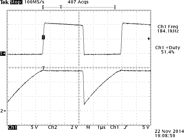
This capture was taken under an 83 mA test load.
A convenient benefit to a circuit built from discrete semiconductors is that it can be repurposed for a negative supply voltage simply by replacing P-type semiconductor with N-type and vice versa (obviously, polarized components like electrolytic capacitors must also be flipped). Here is the circuit diagram as we built it:

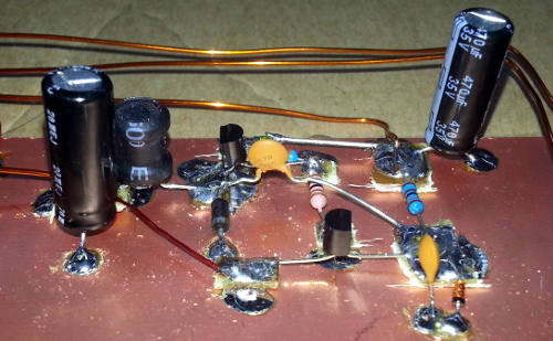
This is the prototype, built with through-hole components on raw copper-clad FR4:
Performance was identical to the +5V regulator.
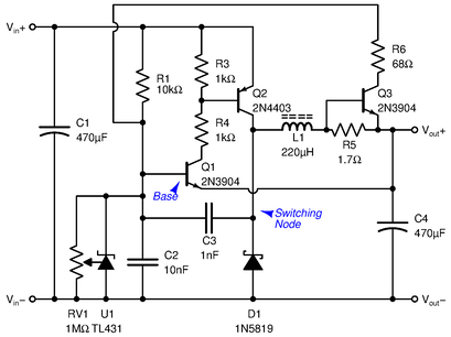
The +3.3V regulator was based on the original design, with two (different) modifications. First, a TL431 programmable shunt reference was used in place of a Zener diode. This was entirely due to availability; if the circuit is used in the final product we will use a normal Zener diode. Second, a different current limiter was used: a sense resistor causes an additional transistor to abort the switching cycle early when the inductor's current reaches a limit. Here is the circuit diagram as we built it:
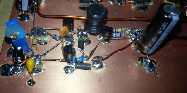
This is the prototype, built with through-hole components on raw copper-clad FR4:
The initial load of the synthesizer board, before the PLL has been enabled, is about 50 mA. At this load current, the DC-DC converter runs in discontinuous mode, where the inductor only conducts current in brief pulses. Here is a plot of the current through the inductor, and the voltage at the switching node (labeled "Switching Node" on the schematic). The node first rises to 10V (driven by the switching transistor), then falls to -0.5V (driven by the switching diode), then returns to the output voltage (ringing in damped resonance with the output capacitor).
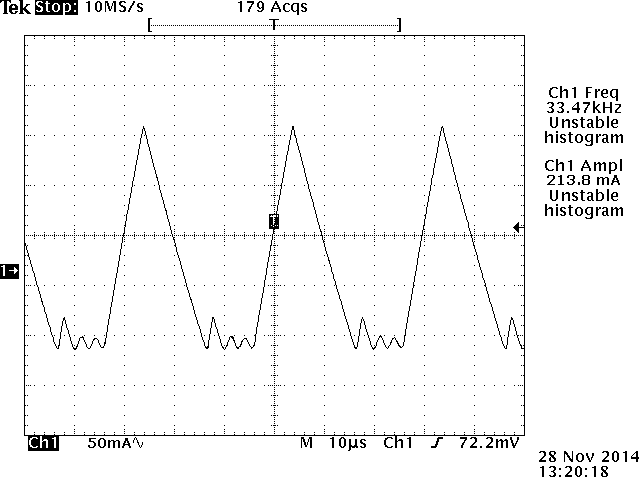
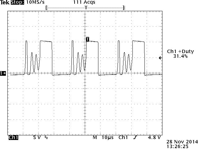
Normally, it would be desirable to add additional damping to the circuit to prevent that ringing, which could inject noise into the load circuit. However, as soon as the PLL is activated (and it will always be active during system operation), the DC-DC converter switches to continuous mode:
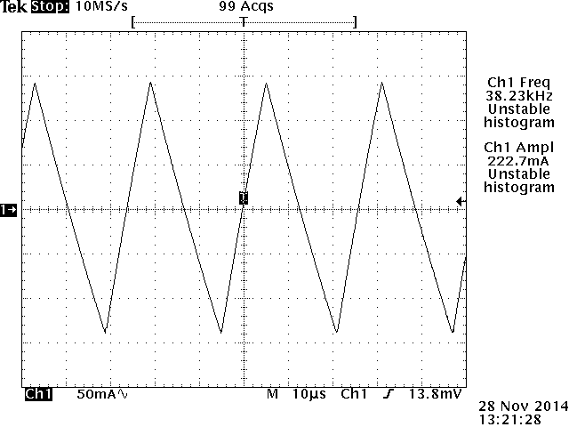
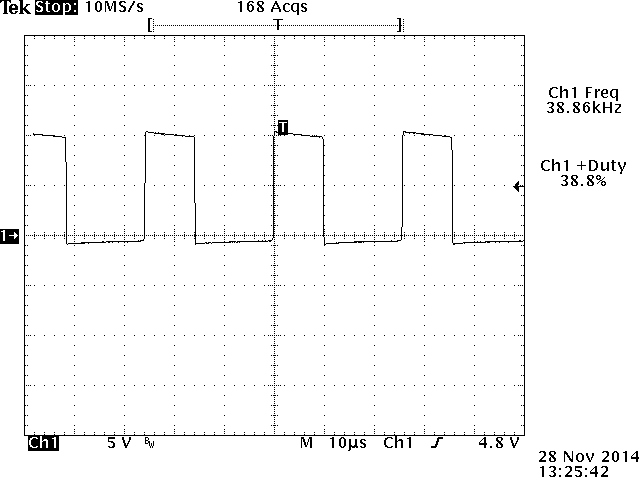
Now, the current through the inductor never falls to zero, and the ringing never occurs.
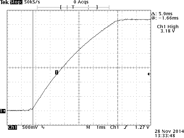
Some DC-DC circuits are prone to overshoot on startup; the output voltage rises to above the desired level briefly. This can damage circuits if not controlled. Here is a plot of the startup of the +3.3V regulator. It rises smoothly from 0 V to 3.3 V in 5.9 ms; no overshoot is visible:
