Frontend Prototype - WCP52/docs GitHub Wiki
Git repository: WCP52/input_frontend
Our input frontend must take the signals from the front-panel input connectors and present them in a form which can be directly sampled by the microcontroller's analog-to-digital converter.
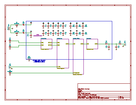
The signals first pass through a simple input protection circuit. This consists of a small-footprint SMD fuse in series with the input and a clamping arrangement set around 3.3V (23 dBm peak).
After the input protection, the two input signals enter a switching circuit to select between them. This allows all of the following circuitry to be shared between channels, miminizing cost and inter-channel variation.
This is followed by a buffer, which isolates the input signal from the following power combiner and filter. After that, a power combiner adds in a variable phase reference, which allows the system to measure the input signal's phase, and a filter cuts the signal off at 300 MHz.
The filtered signal then passes into a logarithmic detector with integrated lowpass filter, which presents a voltage proportional to the logarithm of the input amplitude to the microcontroller.
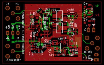
Layer renders: top, inner2, inner3, bottom
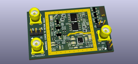
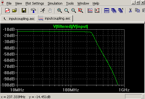
The circuit has not yet been built; these measurements are taken from simulation.
Insertion gain of entire frontend (not including source termination):
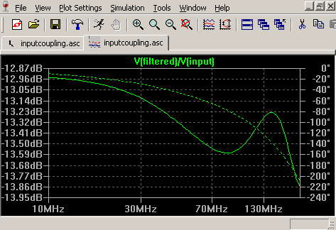
Insertion gain of entire frontend inside passband:
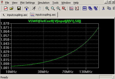
Theoretical VSWR of input (accounting for package capacitances and inductances, not accounting for layout). See VSWR on Microwaves101, and VSWR in LTspice.
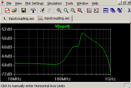
Isolation from phase reference power combiner, as seen at input:
The input protection circuit consists of a simple bidirectional diode clamp.
The ESD9L5.0ST5G from ON Semiconductor was chosen for its very low capacitance
(0.5 pF) and pulse handling capability (as it was designed for ESD protection).
For a more precise cutoff with minimal distortion, these were placed in series
with 2.7V Zener diodes, which were prebiased with a ~2mA current using 1k
resistors. This clamps the input voltage to between 3.2V and 3.4V, causing a
maximum power dissipation of (3.4 V)^2 / 200 = 58 mW in each of the four
200 ohm termination resistors.
Our signal range is too high for conventional analog switches (200 MHz) and too low for conventional diode switching networks (1 kHz). It is possible, of course, to split the signal into two bands, switch them separately, and recombine them; we opted not to do this for simplicity. We used the MASWSS0162 GaAs switch, which is DC-coupled, instead. Its high bandwidth (2.5 GHz) is useful as it brings with it a higher isolation at our frequencies, and it allows very large signal amplitudes (up to around 20 dBm without clipping and around 32 dBm absolute).
See our RF switch characterization log for more information about this device.
The signal is to be mixed with a variable phase reference; this needs to be blocked from traveling back out the inputs and affecting the device under test. The signal is buffered using a BFR540 NPN transistor; the extremely wide bandwidth (9 GHz) brings a higher isolation, both from base to emitter (blocking the phase reference) and from base to collector (reducing input capacitance and improving input matching).
To keep power dissipation to a reasonable level, an active, constant-current load was used instead of a resistor.
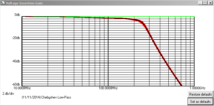
The detector is sensitive well above the frequencies with which we are concerned, so a low-pass filter was used to block everything above 300 MHz. The free AADE Filter Design and Analysis package from Almost All Digital Electronics was used to design a Chebyshev filter (sharp cutoff; passband ripple can be compensated in software) that gives a good response:
The red areas around the curve represent a Monte Carlo analysis assuming 1% capacitor tolerance and 2% inductor tolerance.
The signal is converted to a decibel level by the AD8310 logarithmic amplifier. This is a differential-input device, operating up to 400 MHz and down arbitrarily low.
The termination resistance is 53.6 ohms in parallel with 2.2 kOhms. This is in
parallel with the input impedance of the AD8310, yielding an equivalent
impedance of 1/( 1/53.6 + 1/2.2k + 1/1k ) ~= 49.7. Using one single
resistor of value 52.6 would give almost exactly the same impedance, but both
53.6 and 2.2k were already in use on another board. This keeps our parts list
short and simplifies the build. The error on this impedance is -0.55%.
It is possible to supply a signal to the AD8310 using direct coupling, but the
device is extremely sensitive to offsets, making this unnecessarily difficult.
Capacitive coupling was used instead. A value of 680 nF was selected, which
when combined with the 1 kOhm input impedance of the AD8310 yields a cutoff
frequency of 1/(2 pi (680 nF) (1 kOhm)) ~= 234 Hz, well below our lower
limit of 1 kHz. There will still be some amplitude error at the lowest end,
but this will be software compensated.
For coupling capacitors, we selected TDK C2012JB1E684K125AA. This has a minimal (± 2%) DC bias error at the approximately 3V bias it will experience. Given the impedance-vs-frequency plot of the device, it should be sufficient by itself all the way to 200 MHz (this is past its self-resonant point, but the magnitude of the impedance remains under 1 ohm); a high-frequency 10 nF, size 0402 capacitor was placed in parallel anyway to ensure good high-frequency response. This gives a worst-case gain error of -230 mdB at 1 kHz, and no worse than -70 mdB from 10 kHz to 200 MHz.
Due to its very high gain (86 dB -- datasheet pg. 9), the AD8310 is very
sensitive to offset. An offset of even 1 mV, for example, is equivalent to (and
drowns out) a signal amplitude of -30 dBV. This requires a closed-loop offset
correction. This correction is built into the chip; its corner frequency is by
default 2 MHz, and may be set lower by attaching a capacitor between the
OFLT pin and ground, according to eqn. 12 from pg. 18: fc = 1/( 5250 pi
Coflt ). A 330 nF capacitor yields a corner frequency of 184 Hz, preventing
our 1 kHz minimum frequency from being 'corrected' as an offset.
The output bandwidth of the AD8310 is nominally 25 MHz (page 18); this may be
set lower by attaching a capacitor between the BFIN pin and ground,
according to eqn. 11 from pg. 18: Cfilt = 1/( 2 pi 3kOhm BW ) - 2.1 pF. Our
digital-to-analog converter samples at 1 MHz; a capacitor of 220 pF gives a
bandwidth of 239 kHz, putting the input bandwidth at just above half the
Nyquist rate. We do not require more margin below Nyquist, as we do not need to
sample the signal waveform accurately; we only require an accurate average
amplitude.
It would be possible to select a huge capacitor which places the bandwidth outside our operating frequency range. For example, 1 uF would yield an output bandwidth of 53 Hz. However, this would severely limit the settling time, which would make high-frequency measurements just as slow as low-frequency ones. This is unnecessary, because as long as the A/D converter can sample the signal, we can use software averaging to add a frequency-dependent cutoff.
The AD8310 requires a single rail between 2.7 V and 5.5 V, and draws about 8 mA. We opted to use a 5 V rail, which is likely to be present in the final design. We filtered this using a ferrite bead, and added a 49.9 ohm resistor (already in our bill of materials) to augment the filtering at low frequencies. This will drop approximately 400 mV at the 8 mA operating current, giving a supply voltage of 4.6 V.
