Component and PCell Layout - SiEPIC/SiEPIC_EBeam_PDK GitHub Wiki
DevRec, PinRec
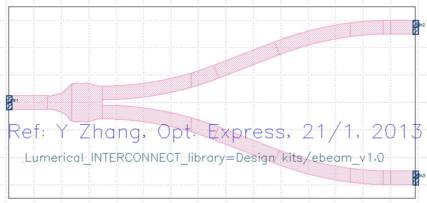
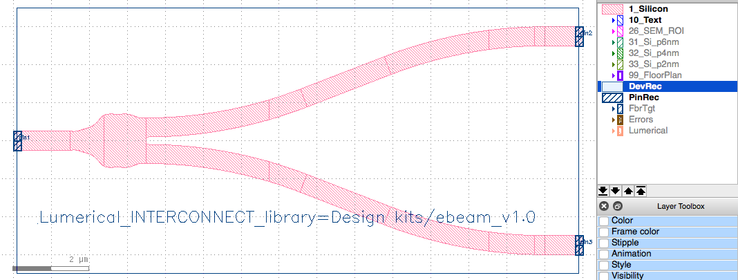
Here is an example component with all the necessary DevRec and PinRec marking shapes and text labels. These are necessary to enable the circuit verification and netlist extraction for simulations.
Purpose of DevRec, PinRec:
The purposes of the DevRec and PinRec layers are to:
-
enable interactive waveguide routing. Components and pins are recognized via geometries contained within a DevRec polygon. A database is created by scanning the GDS and making a list of all components that can be routed to.
-
enable Lumerical INTERCONNECT circuit simulations. DevRec defines the extent of the photonic component. For example, a YBranch has 3 optical input/outputs (defined via the PinRec), and is surrounded by DevRec. In Lumerical FDTD simulations, we can convert the DevRec into a simulation boundary condition (e.g., PML) and generate S-Parameters by placing the simulation Ports (PinRec) layers just slightly inside the DevRec/PML box.
Steps to create a component:
-
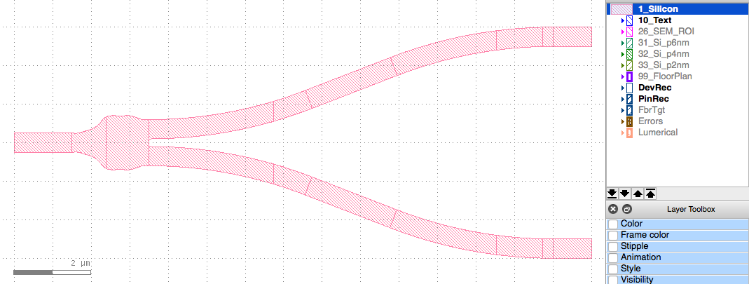
Shapes to be fabricated, drawn on silicon layer
-
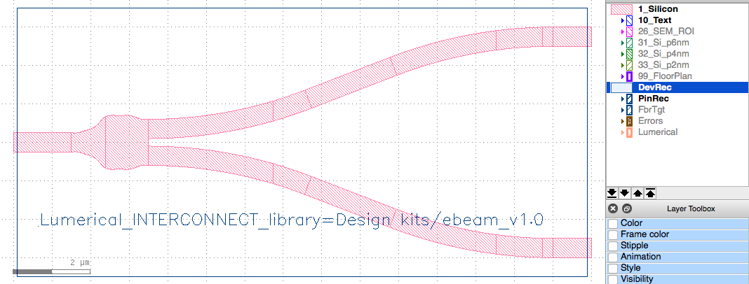
Device Recognition layer – DevRec. We need two shapes:
- A Box or Polygon shape surrounding the component.
- A Text shape, providing a path to the Lumerical INTERCONNECT model library. The component name (cell name) must match the component name in the library.
-
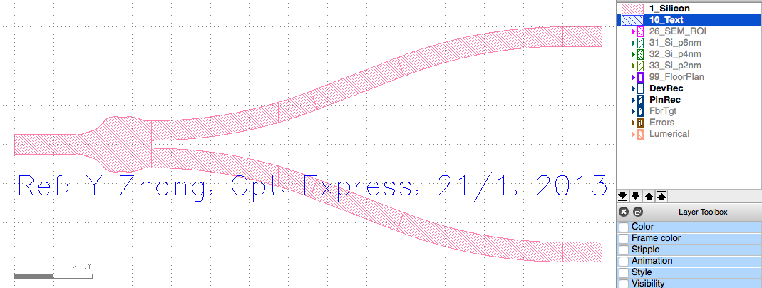
Text description for this component. Ideally a journal paper reference. Placed on the Text layer.
-
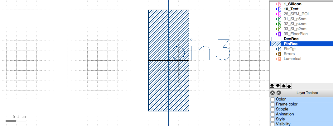
OPTICAL PINS - Pin Recognition layer - PinRec. We need two shapes:
- A Path shape (only) identifying the pin. The waveguide will be snapped along the path, and at the mid-point. Do not use a Polygon or a Box for this. The Path is necessary since a) it provides information on the direction the waveguide must go, b) it makes it very easy to detect offset pin-to-waveguide connections and width mismatches. The Path is used to identify it as an optical pin.
- The pin directions in all components must be consistent so that we can identify which pins can cannot to with other ones. By convention, we define that the path indicates which way the signal is LEAVING the component (path starts with the point inside the DevRec, then the point outside).
- A Text shape, with the name of the pin. It must be located exactly in the mid-point of the Path shape. The pins are exported in the netlist by alphabetical order. Typically numbered left to right, top to bottom. The pin order must match in the Lumerical Compact Model Library (CML).
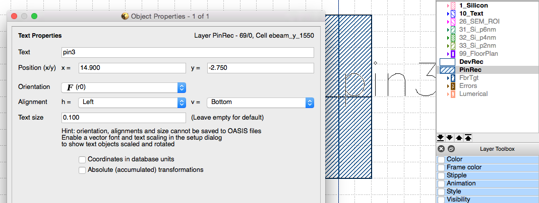
 Details on the PinRec Text pin label:
 Details on the PinRec Path pin shape:
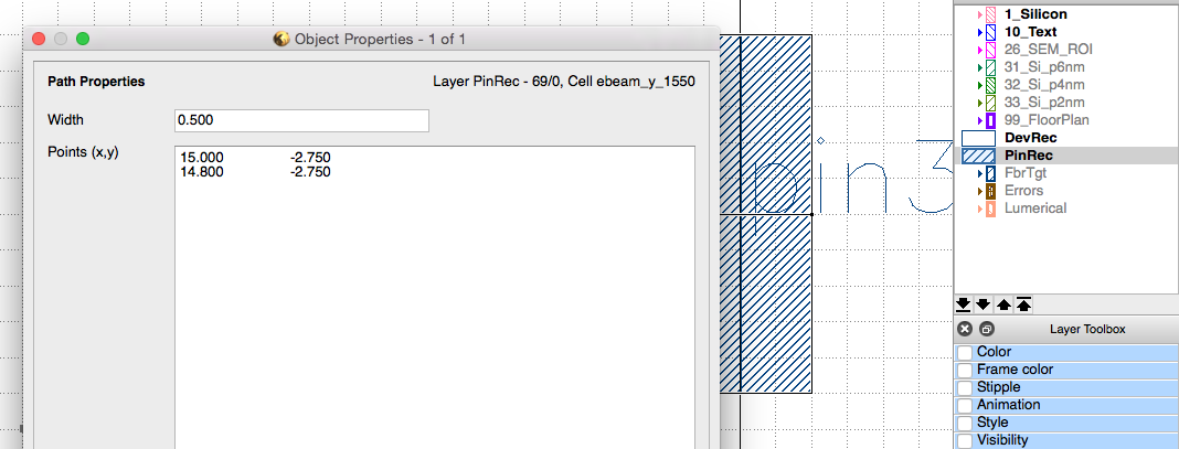 Note that we require that the pin text label be at the midpoint of the path. We recommend having the DevRec crossing through the same midpoints of all pins.
- ELECTRICAL PINS - Pin Recognition layer - PinRec. We need two shapes:
- A Box shape (only) identifying the pin. Do not use a Path for this. The Box is used to identify it as an electrical pin.
- A Text shape, with the name of the pin. It must be located inside the Box shape. The pins are exported in the netlist by alphabetical order. The pin order must match in the Lumerical Compact Model Library (CML).
Notes on hierarchy within components
Hierarchy is permissible, however, all the DevRec and PinRec shapes must be in the component top cell.