Buffer amplifier - SA5NNN/VLF-Receiver GitHub Wiki
Buffer amplifier circuit using BJT
The buffer amplifier creates a relatively high input impedance and low output impedance. This avoids the problem in electronics when low impedance loads the output of another circuit such that it does not function as designed. In other words it provides impedance matching.
There are several variations and you can also use MOSFETs or OP-amps, BJT is not going to going to be able to compete with MOSFET or OP-amps as they have naturally very high input impedance, but often BJT is good enough and certainly very simple to do and cheap as well.
Consider the following circuit:
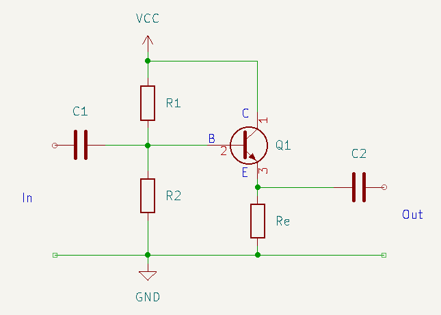 Figure 1
C1 and C2 block DC from our circuit but allows the signal to buffer in and out. Q1 is a NPN transistor such as BC547B. R1 and R2 are a bias network for setting the Q point or quiescent point for the base of Q1. Re limits the current Ic.
The transistor circuit is called emitter follower, voltage follower or common collector. It's amplification is slightly below one, but is considered to have unity gain, that is 1x amplification.
Unloaded input impedance $Z_{in} = R_1 \parallel R_2 \parallel h_{fe} r_e + (h_{fe} + 1) R_E$ where $h_{fe}$ denotes the small signal current gain.
Unloaded output impedance $Z_{out} = R_E \parallel r_e$ where $r_e$ is the internal base-emitter junction resistance.
-> $r_e \approx \frac{0.025}{I_E}$, this requires transistor Q-point set correctly and room temprature.
It can be designed using the following procedure:
- Calulate $V_B$ as $\frac{V_{CC} - V_{BE}}{2}$, this gives the Q-point or quiescent point a DC bias to allow the input signal the maximum swing. $V_{BE}$ can be had from the datasheet. It is usually around 0.7 V (a junction voltage drop).
- Use the fact that $V_B = V_{CC} (\frac{R_2}{R_1 + R_2})$ and assign either R1 or R2 a value to calculate the other. $R_1 \parallel R_2$ often sets $Z_{in}$ since $h_{fe} r_e + (h_{fe} + 1) R_E$ becomes very large. If you want 50 k Ohm, maybe guess $R_1 = 100 kOhm$.
- Calculate $R_E = \frac{V_E}{I_E}$ where $V_E = V_B - V_{BE}$. Select $I_E$ from a datasheet, i.e. 10 mA.
The capacitors C1 and C2 blocks DC but also form a first order analog high pass filter:
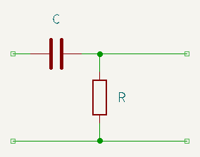 Figure 2
The cutoff frequency $f_c = \frac{1}{2 \pi R C}$. For the input side C is C1 and R is $Z_{in}$ and for the output side C is C2 and R is $Z_{out}$.
At $f_c$ 70.7% of the source voltage has been filtered away. Since they act as high pass filters, $f_c$ must be below the frequence of the signals we are interested in, otherwise if $f_c$ is higher it will filter away the signal of interest.
We can rewrite the formula as $C = \frac{1}{2 \pi R f_c}$, we can then design the capacitors as:
- $C1 = \frac{1}{2 \pi Z_{in} f_c}$ and
- $C2 = \frac{1}{2 \pi Z_{out} f_c}$
You need to decide what frequence you want and maybe add a small margin by using a somewhat smaller value of $f_c$.
An example
Lets look at a real world example and se if we can use the guide above. Lets first consider figure 1:
We assume $V_{CC}$ is 9 V and Q1 is a NPN transistor, BC547B, you can look up the datasheet yourself and follow along.
- First we set Q point, $V_{BE}$ from datasheet:
 I think we might use $I_C$ 10 mA, maybe we can use 660 mV then. $V_B = \frac{9 - 0.66}{2} = 4.17 V$.
 - Ok so $V_B = V_{CC} (\frac{R_2}{R_1 + R_2})$ gives us, $4.17 = 9 (\frac{R_2}{R_1 + R_2})$.
I want around 50 kOhm in input impedance so lets try with 100k for $R_1$.
Lets rewrite the formula and we get $R_2 = \frac{V_B R_1}{V_{CC} - V_B} = \frac{4.17 * 100000}{9 - 4.17} = 86335$ Ohm. - $R_E$: Well, we need $I_E$ from the datasheet:
 There is no $I_E$ but $I_C$ is maximum 100 mA. That is fine because if you think about it, $I_E$ and $I_C$ will be very similar. So what shall we use? Well we need enough current for the load we attach, but also not good if we drain a battery if we are battery powered. I think 10 mA is a good start.
We can always go back and change this if we are not happy with the final result.
There is no $I_E$ but $I_C$ is maximum 100 mA. That is fine because if you think about it, $I_E$ and $I_C$ will be very similar. So what shall we use? Well we need enough current for the load we attach, but also not good if we drain a battery if we are battery powered. I think 10 mA is a good start.
We can always go back and change this if we are not happy with the final result.
$R_E = \frac{V_E}{I_E}$ where $V_E = V_B - V_{BE}$ so now we get $R_E = \frac{V_B - V_{BE}}{I_E} = \frac{4.17 - 0.66}{0.01} = 351$ Ohm. - We now have all resistors, $R_1 = 100$ kOhm, $R_2 = 86$ kOhm and $R_E = 350$ Ohm. With this information we can actually do some usefull calculations of the amplifier and get to know it. This is also needed for the capacitor calculations that still remains to do. For unloaded impedance we need some more info from the datasheet, e.g. $h_{fe}$ and $r_e (=\frac{0.025 V}{I_E})$. $I_E = 10$ mA we already decided from the datasheet above.
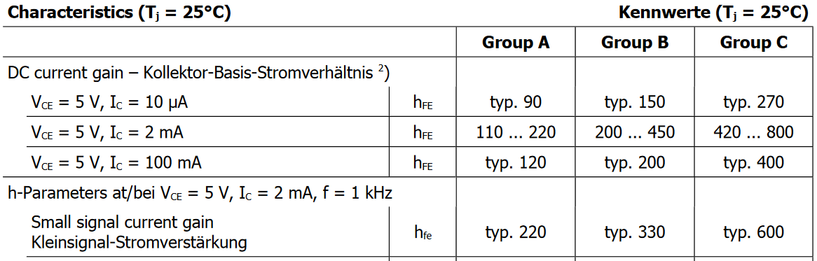 We have type B transistor, $h_{fe}$ is typically 330, lets use that.
 - Unloaded input impedance $Z_{in} = R_1 \parallel R_2 \parallel h_{fe} r_e + (h_{fe} + 1) R_E = 100k \parallel 86k \parallel 330 \frac{0.025}{0.01} + (330 + 1)351 =$
$= 100k \parallel 86k \parallel 117k = 33$ kOhm. - Unloaded output impedance $Z_{out} = R_E \parallel r_e = 350 \parallel \frac{0.025}{0.01} = 350 \parallel 2.5 = 2.48$ Ohm.
- Next we take a look at input cap C1, we know $C1 = \frac{1}{2 \pi Z_{in} f_c}$ but what is $f_c$, I design for SAQ, so 17.2 kHz is my center frequency. I'd like to go as low as 5 kHz and then I think I also have a bit of margin, that gives $C1 = \frac{1}{2 \pi * 33000 * 5000} = 965$ pF.
965 pF is almost 1 nF and pretty small, lets test something a bit bigger, 100 nF for example gives us $f_c$ of 48 Hz. That is definatly low enough, we can go with such a normal cap and still be able to hear att the way down to 5 Hz, so let's go for C1 = 100 nF. - Analogically $C2 = \frac{1}{2 \pi Z_{out} f_c} = \frac{1}{2 \pi * 2.48 * 5000} = 1.3 \mu F$. 1.3 uF is not much either, what happens if we choose something a bit larger here also, lets say 22 uF. We then get $f_c = 2917$ Hz. This is not five hearz but a lot more margin to 5kHz. We select 22 uF for C2.
Ok, so the design is done, we have the following component values: R1 = 100 kOhm R2 = 86 kOhm Re = 350 Ohm C1 = 100 nF C2 = 22 uF
We calculate from these component:
Zin = 33 kOhm
Zout = 2 Ohm
Cutoff frequencies 48 Hz on input and 2.9 kHz on the output.
Voltage gain is $R_e$/($r_e$ + $R_e$) = 351 / (2 + 351) = 0.994, very close to unity gain.\
In the calculations you may have noticed that certain terms add very little, almost nothing, to the end result. If may be pratical to rewrite those formulas so that they are easier to use. E.g. $Z_{in}$ has $h_{fe}$ + 1, but $h_{fe}$ is always a few hundred, so adding 1 before multiplying adds very little. Also the term $h_{fe}$ * $r_e$ adds very little compared to the $h_{fe}$ * $R_e$ so you may want to skip that as well. For $Z_{out}$ one observes that $r_e$ << $R_e$, here 2 vs 351. Therefore $Z_{out}$ could be written simply as $r_e$.