NP1500 Hardware - OpenNoah/OpenNoah.github.io GitHub Wiki
Overview
There are 2 variants of NP1500, codenamed np1500 and np1501 (newer). The only known difference is NAND chips.
| Codename | Serial number prefix | Version (NAND) |
|---|---|---|
| np1500 | 1621 | HY (SK Hynix) |
| np1501 | 1622 / 1701 | SM (Samsung) |
| Hardware | Part number | Features |
|---|---|---|
| CPU | Ingenic JZ4740 PM DS | 336MHz JzRISC 32bits (mipsel) |
| SDRAM | HY57V561620FTP-6 | 64MiB (2x 4Banks x 4M x 16bits) |
| NAND (np1500) | Manufacturer ID: 0xad, Chip ID: 0xd3 | 2GiB (2x 4096Blocks x 128Pages x (2k+64)Bytes) |
| NAND (np1501) | K9GAG08U0M | 2GiB (4096Blocks x 128Pages x (4k+128)Bytes) |
| LCD | PT035TN01-v3 | 320x240 8-bit RGB mode |
Interfaces
| Interface | Availability | Comment |
|---|---|---|
| UART | UART0 | ttyS0 default: 115200bps, 8n1 |
| JTAG | Yes | |
| Boot select | Yes | USB boot working |
Matrix keypad layout
| PD2 | PD3 | PD15 | PD17 | PD30 | PD31 | |
|---|---|---|---|---|---|---|
| PC17 | Back (Top) | PgUp/A (Top) | Menu | C / | D # | R 4 |
| PD0 | Right (Top) | Left (Top) | Shift | X > | Z < | E 3 |
| PD1 | Down (Top) | Up (Top) | IME | V ? | F % | T 5 |
| PD4 | - | W 2 | Del | M \ | J * | I 8 |
| PD5 | - | S @ | Caps | N ; | H . | U 7 |
| PD6 | - | A ! | Sound | ' " | K ( | O 9 |
| PD7 | - | Q 1 | Back | Enter | L ) | P 0 |
| PD14 | Enter (Top) | PgDown/B (Top) | Space | B : | G , | Y 6 |
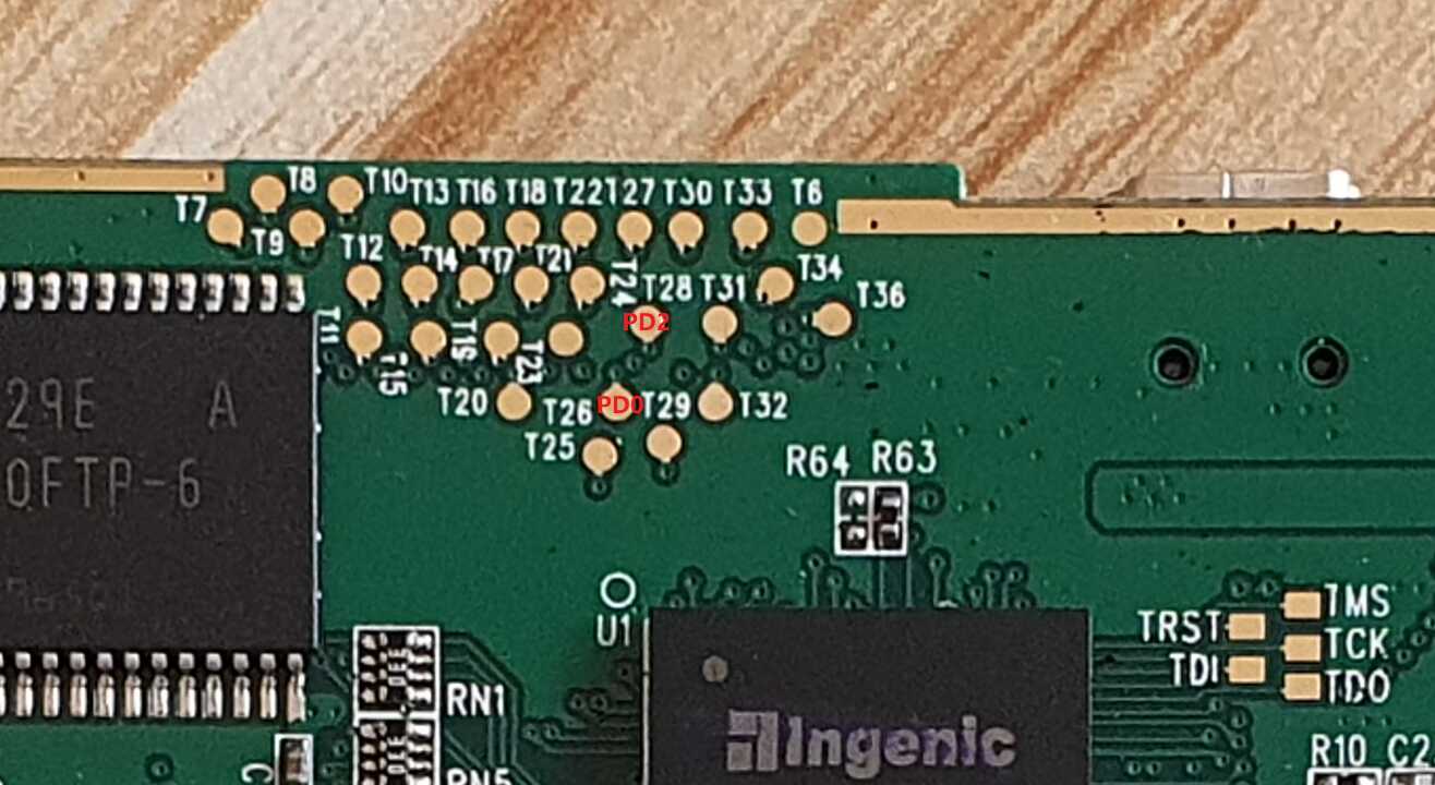
Right (Top) key PCB test point location
WLAN card interface
| GND | 5V | PC9 | PD21 | PC11 | PC16 | PD19 | PD20 |
|---|---|---|---|---|---|---|---|
| GND | 5V | PC15 | PC13 | PC14 | PC12 | PD18 | PC10 |

GPIO configuration
| Group | Config | Function |
|---|---|---|
| PA0-PA31 | AF0 | Memory controller: Data bus |
| PB0-PB16 | AF0 | Memory controller: Address bus |
| PB17-PB18 | OUTPUT, HIGH | ? |
| PB19-PB24 | AF0 | Memory controller: SDRAM specific |
| PB25-PB26 | AF0 | Memory controller: Chip select |
| PB27 | INT, HIGH/LOW | MMC/SD detection, 1: Present |
| PB28 | INPUT, HIGH | ? |
| PB29 | INT, HIGH | ? |
| PB30 | INPUT, HIGH | Polling? |
| PB31 | AF0 | Memory controller: Write enable 0 |
| PC0-PC7 | AF0 | LCD controller: Data bus |
| PC8 | INPUT, HIGH | ? |
| PC9 | INPUT, HIGH | WLAN port |
| PC10-PC11 | INPUT, LOW | WLAN port |
| PC12 | OUTPUT, HIGH | WLAN port |
| PC13-PC16 | INPUT, HIGH | WLAN port |
| PC17 | IO | Matrix keyboard column |
| PC18-PC20 | AF0 | LCD controller: Clock & sync |
| PC21 | OUTPUT | LCD enable, 1: on |
| PC22 | OUTPUT, LOW | ? |
| PC23 | INPUT, HIGH | ? |
| PC24-PC26 | AF0 | Memory controller: Write enable 1-3 |
| PC27 | OUTPUT | MMC/SD power, active low |
| PC28-PC29 | AF0 | Memory controller: NAND RD&WR enables |
| PC30 | INPUT | Memory controller: NAND ready/busy |
| PC31 | INPUT | JTAG(SEL=0)/UART(SEL=1) select |
| PD0-PD1 | IO | Matrix keyboard column |
| PD2-PD3 | IO | Matrix keyboard row |
| PD4-PD7 | IO | Matrix keyboard column |
| PD8-PD13 | AF0 | MMC/SD controller |
| PD14 | IO | Matrix keyboard column |
| PD15 | IO | Matrix keyboard row |
| PD16 | INPUT, HIGH | ? |
| PD17 | IO | Matrix keyboard row |
| PD18-PD21 | AF0 | WLAN port, SSI |
| PD22-PD24 | INPUT, HIGH | ? |
| PD25-PD26 | AF1 | UART0 |
| PD27 | AF0/OUTPUT | PWM4 output, LCD backlight |
| PD28 | OUTPUT, LOW | ? |
| PD29 | AF1/0 | Power button, 0: Pressed |
| PD30-PD31 | IO | Matrix keyboard row |