wiki - KS10FPGA/KS10FPGA GitHub Wiki
The KS10 FPGA Project
Copyright 2023
Rob Doyle
doyle (at) cox (dot) net
1 The KS10 FPGA Project
1.1 Project Goals
1.2 The DEC KS10
1.3 The KS10 FPGA
1.4 KS10 FPGA Status
1.5 DEC KS10 Documentation
2 The Host Computer System
2.1 Cloning the KS10 FPGA Github Repository
2.2 The Installation Tree
2.3 Building the Console Processor Executable
2.3.1 Cygwin Software Build
2.3.2 Windows Subsystem for Linux (WSL) Software Build
2.3.3 On Target Software Build
2.4 FPGA Firmware Tooling
2.4.1 Quartus 18.1 for Windows FPGA Firmware Build Process
2.4.2 Quartus 21.1 for Windows FPGA Firmware Build Process
2.4.3 Quartus 21.1 for Linux/WSL FPGA Firmware Build Process
2.5 Building the FPGA Firmware
2.5.1 FPGA Firmware Build Rules
2.6 Building the Custom KS10 Development Tools
2.6.1 asm10
2.6.2 tapeutils
2.6.3 sav2verilog
2.6.4 Merge18 and merge36
2.7 Co-simulating the FPGA RTL and PDP-10 Software
2.7.1 Simulating with ModelSim
2.7.1.1 ModelSim Limitations
2.7.2 Simulating with QuestaSim
2.7.3 Simulation using Icarus Verilog
2.7.4 Co-simulating FPGA and PDP-10 Software
2.7.5 Extracting the RED PACK from Magtape
2.8 Extracting the KS10 Diagnostics from Magtape
2.9 Initializing the RP06 Disk Drives
2.9.1 Background
2.9.2 Disk Partitioning
2.9.3 Disk Formatting
2.9.4 Cygwin Programming Procedure
2.9.4.1 Step 1: Select the disk device
2.9.4.2 Step 2: Programming the selected disk device
2.9.5 WSL Programming Procedure
2.9.6 Linux Programming Procedure
3 Console Processor
3.1 Status
4 Console Hardware
4.1 Target Hardware
4.1.1 DE10-NANO Development Kit
4.1.2 Intel Cyclone 5 System on a Chip
4.1.3 KS10 FPGA Daughter Board
4.1.4 USB Hub
4.2 Schematic and PWB Layout Design Information
4.3 My Target Configuration
4.3.1 WiFi
4.4 Other Issues that needed to be solved.
4.5 Hardware Status
5 BUS: KS10 Backplane Bus Cycles
5.1 BUS: KS10 Address Bus
5.2 BUS: KS10 Data Bus
5.2.1 BUS: KS10 Bus Cycles
5.2.2 BUS: KS10 Memory Read and Write Cycles
5.2.2.1 BUS: KS10 Memory Read Cycle
5.2.2.2 BUS: KS10 Memory Write Cycle
5.2.3 BUS: KS10 IO Read and Write Cycle
5.2.3.1 BUS: KS10 Word IO Read Cycle (36-bit or 16-bit)
5.2.3.2 BUS: KS10 Byte IO Read Cycle
5.2.3.3 BUS: KS10 Word IO Write Cycle (36-bit or 16-bit)
5.2.3.4 BUS: KS10 Byte IO Write Cycle
5.2.4 BUS: KS10 Who Are You (WRU) Cycle
5.2.5 BUS: KS10 Interrupt Vector Cycle
5.3 BUS: KS10 Interrupt Sequence
6 CON: KS10 Console Interface
6.1 CON: KS10 Interface Register Set
6.1.1 CON: KS10 Console Address Register (CONAR)
6.1.2 CON: KS10 Console Data Register (CONDR)
6.1.3 CON: KS10 Console Instruction Register (CONIR)
6.1.4 CON: KS10 Console Control/Status Register (CONCSR)
6.1.5 CON: DZ11 Console Control Register (DZCCR)
6.1.6 CON: LP20 Console Control Register (LPCCR)
6.1.7 CON: Magtape Console Control Register (MTCCR)
6.1.8 CON: RP Console Control Register (RPCCR)
6.1.9 CON: DUP11 Console Control Register (DUPCCR)
6.1.10 CON: KMC11 Control Register (KMCCCR)
6.1.11 CON: KS10 Breakpoint Address Registers (BRAR[0:3])
6.1.12 CON: KS10 Breakpoint Mask Registers (BRMR[0:3])
6.1.13 CON: KS10 Instruction Trace Register (ITR)
6.1.14 CON: PC and IR (PCIR) Registers
6.1.15 CON: MT Data Interface Register (MTDIR)
6.1.16 CON: MT Debug Register (MTDEBUG)
6.1.17 CON: RP Debug Register (RPDEBUG)
6.1.18 CON: KS10 Firmware Version Register (FVR)
6.2 CON: KS10 Control Interface
6.2.1 CON: The RUN bit
6.2.2 CON: The CONT bit
6.2.3 CON: The EXEC bit
6.3 CON: KS10 Console Communications Area
6.3.1 CON: KS10 Halt Switch
6.3.2 CON: KS10 Keep Alive Word
6.3.3 CON: KS10 CTY Input Word
6.3.4 CON: KS10 CTY Output Word
6.3.5 CON: KS10 KLINIK Input Word
6.3.6 CON: KS10 KLINIK Output Word
6.3.7 CON: KS10 Boot RH11 Address
6.3.8 CON: KS10 Boot Unit Number
6.3.9 CON: Magtape Parameters
6.4 CON: Console Status
7 KS10: The KS10 FPGA Block Diagram
8 CPU: The KS10 CPU
8.1 CPU: Functional Blocks
8.1.1 CPU: Arithmetic Logic Unit (ALU)
8.1.2 CPU: Arithmetic Processor Flags (APR)
8.1.3 CPU: Backplane Bus Interface (BUS)
8.1.4 CPU: DBM Multiplexer (DBM)
8.1.5 CPU: DBUS Multiplexer (DBUS)
8.1.6 CPU: Byte Dispatch (DISP_BYTE)
8.1.7 CPU: Next Instruction Dispatch (DISP_NI)
8.1.8 CPU: Page Fail / Interrupt Dispatch (DISP_PF)
8.1.9 CPU: Console Interface (INTF)
8.1.10 CPU: Microsequencer (USEQ)
8.1.10.1 CPU: Microsequencer Dispatch (DISPATCH)
8.1.10.2 CPU: Microsequencer Skip (SKIP)
8.1.10.3 CPU: Microsequencer Stack (STACK)
8.1.10.4 CPU: Microsequencer Control ROM (CROM)
8.1.10.5 CPU: Microsequencer Dispatch ROM (DROM)
8.1.11 CPU: Non-existent Device (NXD)
8.1.12 CPU: Non-existent Memory (NXM)
8.1.13 CPU: Pager (PAGER)
8.1.14 CPU: PC Flags (PCFLAGS)
8.1.15 CPU: Priority Interrupt (PI)
8.1.16 CPU: Previous Context (PXCT)
8.1.17 CPU: KS10 RAM File (RAMFILE)
8.1.18 CPU: Instruction Register (IR)
8.1.19 CPU: Step Count Adder (SCAD)
8.1.20 CPU: Interval Timer (TIMER)
8.2 CPU: Performance / DSKFAA0 Benchmark Summary
8.3 CPU: Status
9 MEM: DEC KS10 Memory Controller
9.1 MEM: ADP Modifications to Memory Controller
9.2 MEM: Memory Controller Register Set
9.2.1 MEM: Memory Status Register (MSR)
9.3 MEM: SSRAM Memory Interface
9.3.1 MEM: x18-bit SSRAM Interface
9.3.1.1 MEM: SSRAM Read and Write Cycles
9.3.1.1.1 MEM: SSRAM Read Cycle
9.3.1.2 MEM: SSRAM Write Cycle
9.3.2 MEM: 36-bit SSRAM Interface
9.3.2.1 MEM: SSRAM Read Cycle
9.3.2.2 MEM: SSRAM Write Cycle
9.4 MEM: Status
10 UBA: IO Bus Bridge
10.1 UBA: Register Set
10.1.1 UBA: Status Register (UBASR)
10.1.2 UBA: Maintenance Register (UBAMR)
10.2 UBA: Address Translation (Paging)
10.2.1 UBA: Paging Memory (UBAPAG)
10.2.2 UBA: Page Failure
10.3 UBA: IO Data Translation
10.4 UBA: DSUBA Transcripts
10.4.1 UBA: DSUBA Transcript With No UBEs Attached
10.4.2 UBA: DSUBA Transcript With UBEs Attached
10.5 UBA: Status
11 RH: Massbus Controller
11.1 RH: Register Set Summary
11.2 RH: Massbus Register Set
11.2.1 RH: Control and Status #1 (RHCS1) Register
11.2.2 RH: Word Count (RHWC) Register
11.2.3 RH: Bus Address (RHBA) Register
11.2.4 RH: Control and Status #2 (RHCS2) Register
11.2.5 RH: Data Buffer (RHDB) Register
11.3 RH: Interrupts
11.4 RH: Status
12 RP: Massbus Disk Controller (RP)
12.1 RP: Massbus Disk Controller Implementation
12.2 RP: Disk Parameters
12.3 RP: Compatibility between Massbus Disk Drives and the SD Card
12.3.1 RP: Sector Size
12.3.2 RP: Sector Addressing
12.3.3 RP: Data Transfer Rates
12.3.4 RP: Seek time and Search Time
12.3.5 RP: Partial Reads and Writes
12.3.6 RP: The RP06 Disk in Detail
12.4 RP: Device Registers Summary
12.5 RP: Register Set
12.5.1 RP: Control and Status #1 Register (RPCS1)
12.5.2 RP: Disk Address Register (RPDA)
12.5.3 RP: Drive Status Register (RPDS)
12.5.4 RP: Error #1 Register (RPER1)
12.5.5 RP: Attention Summary Register (RPAS)
12.5.6 RP: Look Ahead Register (RPLA)
12.5.7 RP: Maintenance Register (RPMR)
12.5.8 RP: Drive Type Register (RPDT)
12.5.9 RP: Serial Number Register (RPSN)
12.5.10 RP: Offset Register (RPOF)
12.5.11 RP: Desired Cylinder Register (RPDC)
12.5.12 RP: Current Cylinder Register (RPCC)
12.5.13 RP: Error Status #2 Register (RPER2)
12.5.14 RP: Error Status #3 Register (RPER3)
12.5.15 RP: Error Position Register (RPEC1)
12.5.16 RP: Error Pattern Register (RPEC2)
12.6 RP: Functions
12.7 RP: Status
12.8 RP: Emulated Disk Benchmarks
13 MT: Massbus Tape Controller (MT)
13.1 MT: Device Registers Summary
13.2 MT: Register Set
13.2.1 MT: Control and Status #1 Register (MTCS1)
13.2.2 MT: Frame Count Register (MTFC)
13.2.3 MT: Drive Status Register (MTDS)
13.2.4 MT: Error Register (MTER)
13.2.5 MT: Attention Summary Register (MTAS)
13.2.6 MT: Character Check Register (MTCC)
13.2.7 MT: Maintenance Register (MTMR)
13.2.8 MT: Drive Type Register (MTDT)
13.2.9 MT: Serial Number Register (MTSN)
13.2.10 MT: Tape Control Register (MTTC)
13.3 MT: Functions
13.4 MT: Data Interface Register (MTDIR)
13.5 MT: Timing Parameters
13.6 MT: Console Processor Software
13.6.1 MT: Beginning of Tape (BOT)
13.6.2 MT: End of Tape (EOT)
13.7 MT: Tape Formatting
13.7.1 MT: Tape Format: PDP-10 Core Dump Format
13.7.2 MT: Tape Format: PDP-10 Seven Track Format
13.7.3 MT: Tape Format: PDP-10 ASCII Format
13.7.4 MT: Tape Format: PDP-10 Compatible Format
13.7.5 MT: Tape Format: PDP-11 Normal Tape Format
13.7.6 MT: Tape Format: PDP-15 Normal Tape
13.8 MT: RH11/TM03/TU45 Status
13.8.1 MT: Diagnostic Transcripts
13.8.1.1 MT: DSTUA Basic Device Diagnostic Results
13.8.1.2 MT: DSTUB Reliability Diagnostic Results
13.8.2 MT: Status
14 DZ: Terminal Multiplexer
14.1 DZ: DZ11 Register Set
14.1.1 DZ: Control and Status Register (DZCSR)
14.1.2 DZ: Receiver Buffer Register (DZRBUF)
14.1.3 DZ: Line Parameter Register (DZLPR)
14.1.4 DZ: Transmit Control Register (DZTCR)
14.1.5 DZ: Modem Status Register (DZMSR)
14.1.6 DZ: Transmit Data Register (DZTDR)
14.2 DZ: Interrupts
14.2.1 DZ: Transmitter Interrupt
14.2.2 DZ: Receiver Interrupt
14.3 DZ: Status
15 LP: LP20 Printer Controller
15.1 LP: LP20 Registers
15.1.1 LP: Control/Status A Register (LPCSRA)
15.1.2 LP: Control/Status B Register (LPCSRB)
15.1.3 LP: Bus Address Register (LPBAR)
15.1.4 LP: Byte Count Register (LPBCTR)
15.1.5 LP: Page Count Register (LPPCTR)
15.1.6 LP: RAM Data Register (LPRAMD)
15.1.7 LP: Column Counter Register (LPCCTR) / Character Buffer Register (LPCBUF)
15.1.8 LP: Checksum Register (LPCKSM) / Printer Data Register (LPPDAT)
15.2 LP: Interrupts
15.3 LP: Modes
15.3.1 LP: Print Mode
15.3.2 LP: Test Mode
15.3.3 LP: Normal Test Mode
15.3.4 LP: Demand Timeout Test Mode
15.3.5 LP: SSYN Timeout Test Mode
15.3.6 LP: RAM Parity Test Mode
15.3.7 LP: Memory Parity Test Mode
15.3.8 LP: Line Printer Parity Test Mode
15.3.9 LP: Page Counter Test Mode
15.3.10 LP: Load DAVFU Mode
15.3.11 LP: Load Translation RAM Mode
15.4 LP: DSLPA Transcript
15.5 LP: FPGA Status
16 LP: LP26 Printer
16.1 LP: LP26 Characteristics
16.2 LP: LP26 Vertical Format Units
16.2.1 LP: LP26 Tape Controlled Vertical Format Unit (TCVFU)
16.2.2 LP: LP26 Direct Access Vertical Format Unit (DAVFU)
16.2.2.1 LP: LP26 DAVFU Loading
16.2.2.1.1 LP: LP26 DAVFU Start Load Codes
16.2.2.1.2 LP: LP26 DAVFU Stop Load Codes
16.2.2.2 LP: LP26 DAVFU Use
16.2.2.2.1 LP: LP26 DAVFU Absolute Motion (Channel Codes)
16.2.2.2.2 LP: LP26 DAVFU Relative Motion (Slew)
16.2.3 LP: LP26 Error Conditions
17 DUP: DUP11 Synchronous Serial Interface
17.1 DUP: Synchronous Serial Protocols
17.1.1 DUP: SDLC/ADCCP Protocol
17.1.2 DUP: DDCMP/BISYNC Protocol
17.2 DUP: DUP11 Registers
17.2.1 DUP: Receiver Control/Status Register (RXCSR)
17.2.2 DUP: Received Data Buffer (RXDBUF)
17.2.3 DUP: Parameter Control/Status Register (PARCSR)
17.2.4 DUP: Transmitter Control/Status Register (TXCSR)
17.2.5 DUP: Transmitter Data Buffer (TXDBUF)
17.3 DUP: Interrupts
17.3.1 DUP: Receiver Interrupt
17.3.2 DUP: Transmitter Interrupt
17.4 DUP: DSDUA Transcript
17.5 DUP: FPGA Status
18 KMC: KMC11 Microprocessor
18.1 KMC: KMC11 Register Summary
18.1.1 KMC: Control and Status Registers
18.1.2 KMC: Maintenance Register
18.1.3 KMC: Maintenance Address Register
18.1.4 KMC: Maintenance Instruction Register
18.2 KMC: Microprocessor Registers
18.2.1 KMC: NPR Input Data (NPRID) Register
18.2.2 KMC: NPR Output Data (NPROD) Register
18.2.3 KMC: NPR Input Address (NPRIA) Register
18.2.4 KMC: NPR Output Address (NPROA) Register
18.2.5 KMC: CSR0 Register
18.2.6 KMC: CSR1 Register
18.2.7 KMC: CSR2 Register
18.2.8 KMC: CSR3 Register
18.2.9 KMC: CSR4 Register
18.2.10 KMC: CSR5 Register
18.2.11 KMC: CSR6 Register
18.2.12 KMC: CSR7 Register
18.2.13 KMC: NPR Control Register (KMCNPRC)
18.2.14 KMC: MISC Register (KMCMISC)
18.3 KMC: DSKMA Transcript
18.4 KMC: Status
19 UBE: Unibus Adapter Exerciser
19.1 UBE: Interface Registers
19.1.1 UBE: Data Buffer Register (UBEDB)
19.1.2 UBE: Cycle Count Register (UBECC)
19.1.3 UBE: Buffer Address Register (UBEBA)
19.1.4 UBE: Control/Status Register #1 (UBECSR1)
19.1.5 UBE: Clear Error Register (UBECLR)
19.1.6 UBE: Control/Status Register #2 (UBECSR2)
19.1.7 UBE: Simultaneous GO Register (SIMGO)
19.2 UBE: DSUBA Transcript
19.3 UBE: Status
20 DSKFAA0 Benchmark Summary
21 Creating the REDPACK
22 Exploring the REDPACK
23 Building the Microcode
Figure 1 - The DEC KS10
Figure 2 - The DEC KS10 with Covers Removed
Figure 3 - KS10 FPGA in Mini-ITX chassis
Figure 4 - KS10 FPGA Block Diagram
Figure 5 - KS10 FPGA design on Intel Cyclone 5 System on Chip (SoC)
Figure 6 - KS10 FPGA Hardware (Side View)
Figure 7 - KS10 FPGA Hardware (Front View)
Figure 8 - KS10 FPGA Hardware Configuration
Figure 9 - BUS: KS10 FPGA Block Diagram
Figure 10 - BUS: KS10 Address Bus Definition
Figure 11 - BUS: KS10 Memory Read Cycle
Figure 12 - BUS: KS10 Memory Write Cycle
Figure 13 - BUS: KS10 Word IO Read Cycle
Figure 14 - BUS: KS10 Byte IO Read Cycle
Figure 15 - BUS: KS10 Word IO Write Cycle
Figure 16 - BUS: KS10 Byte IO Write Cycle
Figure 17 - BUS: KS10 WRU Cycle
Figure 18 - BUS: KS10 Interrupt Vector Cycle
Figure 19 - CON: KS10 Console Address Register (CONAR)
Figure 20 - CON: KS10 Console Address Register (CONAR) Bit Definitions
Figure 21 - CON: KS10 Console Data Register (CONDR)
Figure 22 - CON: KS10 Console Instruction Register (CONIR)
Figure 23 - CON: KS10 Console Control/Status Register (CONCSR)
Figure 24 - CON: DZ11 Console Control Register (DZCCR)
Figure 25 - CON: LP Console Control Register (LPCCR)
Figure 26 - CON: MT Console Control Register (MTCCR)
Figure 27 - CON: RP Console Control Register (RPCCR)
Figure 28 - CON: DUP11 Console Control Register (DUPCCR)
Figure 29 - CON: KS10 Breakpoint Address Register (BRAR[0:3])
Figure 30 - CON: KS10 Breakpoint Mask Register (BRMR[0:3])
Figure 31 - CON: KS10 Instruction Trace Register (ITR)
Figure 32 - CON: KS10 Program Counter and Instruction Register (PCIR)
Figure 33 - CON: MT Debug Register (MTDEBUG)
Figure 34 - CON: RP Debug Register (RPDEBUG)
Figure 35 - CON: KS10 Firmware Version Register (FVR)
Figure 36 - CON: KS10 Control State Diagram
Figure 37 - CON: KS10 CTY Input Word (KS10 Memory Address 000032)
Figure 38 - CON: KS10 CTY Output Word (KS10 Memory Address 000033)
Figure 39 - KS10: FPGA Block Diagram
Figure 40 - CPU: Block Diagram
Figure 41 - CPU: ALU Implementation (DEC KS10)
Figure 42 - CPU: ALU Implementation (KS10 FPGA)
Figure 43 - CPU: Extended Addressing
Figure 44 - CPU: Physical Addressing
Figure 45 - CPU: Paged Addressing
Figure 46 - CPU: WRU Addressing
Figure 47 - CPU: Bus Interface Block Diagram
Figure 48 - CPU: DBM Block Diagram
Figure 49 - CPU: DBUS Block Diagram
Figure 50 - CPU: Microsequencer Block Diagram
Figure 51 - CPU: Microseqencer Stack
Figure 52 - CPU: Pager Address Translation
Figure 53 - CPU: Pager Block Diagram
Figure 54 - CPU: Priority Interrupt Register
Figure 55 - CPU: Priority Interrupt Block Diagram
Figure 56 - CPU: SCAD Block Diagram
Figure 57 - CPU: Interval Timer Register
Figure 58 - CPU: Interval Timer Block Diagram
Figure 59 - MEM: Memory Status Register (Read)
Figure 60 - MEM: Memory Status Register (Write)
Figure 61 - MEM: Burst Mode SSRAM Address and Data Mapping
Figure 62 - MEM: SSRAM Write Cycle followed by and Read Cycle
Figure 63 - MEM: SSRAM Read Cycle
Figure 64 - MEM: SSRAM Read Cycle Timing Parameters
Figure 65 - MEM: SSRAM Write Cycle
Figure 66 - MEM: SSRAM Write Cycle Timing Parameters
Figure 67 - UBA: Status Register (UBASR)
Figure 68 - UBA: Maintenance Register (UBAMR)
Figure 69 - UBA: Address Translation (Paging)
Figure 70 - UBA: Paging RAM (Write)
Figure 71 - UBA: Paging RAM (Read)
Figure 72 - UBA: Byte and Word Translation into a 36-bit Word
Figure 73 - RH: Control and Status #1 Register (RHCS1)
Figure 74 - RH: Word Count Register (RHWC)
Figure 75 - RH: Bus Address Register (RPBA)
Figure 76 - RH: Control and Status Register #2 (RHCS2)
Figure 77 - RH: Data Buffer Register (RPDB)
Figure 78 - RP: Massbus Disk Controller Block Diagram
Figure 79 - RP: Massbus Disk Addressing
Figure 80 - RP: Control and Status Register #1 (RPCS1)
Figure 81 - RP: Disk Address Register (RPDA)
Figure 82 - RP: Drive Status Register (RPDS)
Figure 83 - RP: Error Register #1 (RPER1)
Figure 84 - RP: Attention Summary Register (RPAS)
Figure 85 - RP: Look Ahead Register (RPLA)
Figure 86 - RP: Maintenance Register (RPMR)
Figure 87 - RP: Drive Type Register (RPDT)
Figure 88 - RP: Serial Number Register (RPSN)
Figure 89 - RP: Offset Register (RPOF)
Figure 90 - RP: Desired Cylinder Register (RPDC)
Figure 91 - RP: Current Cylinder Register (RPCC)
Figure 92 - RP: Error Status #2 (RPER2)
Figure 93 - RP: Error Status #3 (RPER3)
Figure 94 - RP: Error Position Register (RPEC1)
Figure 95 - RP: Error Pattern Register (RPEC2)
Figure 96 - MT: Control and Status Register #1 (MTCS1)
Figure 97 - MT: Frame Register (MTFC)
Figure 98 - MT: Drive Status Register (MTDS)
Figure 99 - MT: Error Register (MTER)
Figure 100 - MT: Attention Summary Register (MTAS)
Figure 101 - MT: Character Check (MTCC)
Figure 102 - MT: Maintenance Register (MTMR)
Figure 103 - MT: Drive Type Register (MTDT)
Figure 104 - MT: Serial Number Register (MTSN)
Figure 105 - MT: Tape Control Register (MTTC)
Figure 106 - MT: Tape Format: PDP-10 Core Dump Format
Figure 107 - MT: Tape Format: PDP-10 Seven Track Format
Figure 108 - MT: Tape Format: PDP-10 ASCII Format
Figure 109 - MT: Tape Format: PDP-10 Compatible Format
Figure 110 - DZ: DZ11 Block Diagram
Figure 111 - DZ: Control and Status Register (DZCSR)
Figure 112 - DZ: Receiver Buffer Register (DZRBUF)
Figure 113 - DZ: Line Parameter Register (DZLPR)
Figure 114 - DZ: Transmit Control Register (DZTCR)
Figure 115 - DZ: Modem Status Register (DZMSR)
Figure 116 - DZ: Transmit Data Register (DZTDR)
Figure 117 - LP: Control/Status Register A (LPCSRA)
Figure 118 - LP: Control/Status Register B (LPCSRB)
Figure 119 - LP: Bus Address Register (LPBAR)
Figure 120 - LP: Byte Count Register (LPBCTR)
Figure 121 - LP: Page Count Register (LPPCTR)
Figure 122 - LP: RAM Data Register (LPRAMD)
Figure 123 - LP: Column Counter Register (LPCCTR) / Character Buffer Register (LPCBUF)
Figure 124 - LP: Printer Data Register (LPPDAT) / Checksum Register (LPCKSM)
Figure 125 - LP: LP26 Printer Photo
Figure 126 - LP: LP26 Printer Data Munging
Figure 127 - DUP: SDLC/ADCCP Protocol
Figure 128 - DUP: DDCMP/BISYNC Protocol
Figure 129 - DUP: Receiver Control/Status Register (RXCSR)
Figure 130 - DUP: Received Data Buffer (RXDBUF)
Figure 131 - DUP: Parameter Control/Status Register (PARCSR)
Figure 132 - DUP: Transmitter Control/Status Register (TXCSR)
Figure 133 - DUP: Transmitter Data Buffer (TXDBUF)
Figure 134 - KMC: Register Set
Figure 135 - KMC: NPR Control Register (KMCNPRC)
Figure 136 - KMC: MISC Register (KMCMISC)
Figure 137 - UBE: Data Buffer Register (UBEDB)
Figure 138 - UBE: Cycle Count Register (UBECC)
Figure 139 - UBE: Buffer Address Register (UBEBA
Figure 140 - UBE: Control/Status Register #1 (UBECSR1)
Figure 141 - UBE: Clear Error Register (UBECLR)
Figure 142 - UBE: Control/Status Register #2 (UBECSR2)
Figure 143 - UBE: Simultaneous GO Register (SIMGO)
Table 1 - BUS: KS10 Bus Arbiter Operations
Table 2 - BUS: KS10 Address Flag Definitions
Table 3 - CON: KS10 Interface Register Inventory
Table 4 - CON: KS10 Console Control/Status Register Definitions
Table 5 - CON: DZ11 Console Control Register (DZCCR) Definition
Table 6 - CON: LP20 Console Control Register (LPCCR) Definitions
Table 7 - CON: MT Console Control Register (MTCCR)
Table 8 - CON: RP Console Control Register (RPCCR)
Table 9 - CON: DUP11 Console Control Register (DUPCCR) Definition
Table 10 - CON: KS10 Breakpoint Address Register (BRAR[0:3]) Definitions
Table 11 - CON: KS10 Breakpoint Mask Register (BRMR[0:3]) Definitions
Table 12 - CON: KS10 Instruction Trace Register (ITR) Definitions
Table 13 - CON: KS10 Program Counter and Instruction Register (PCIR) Definitions
Table 14 - CON: MT Data Interface Register (MTDIR)
Table 15 - CON: MT Debug Register (MTDEBUG) Definitions
Table 16 - CON: RP Debug Register (RPDEBUG) Definitions
Table 17 - CON: KS10 Firmware Version Register (FVR) Definitions
Table 18 - CON: KS10 Control Interface
Table 19 - CON: KS10 Console Communications Area
Table 20 - CON: KS10 Halt Switch (KS10 Memory Address 000030)
Table 21 - CON: KS10 Keep Alive Word (KS10 Memory Address 000031)
Table 22 - CON: KS10 CTY Output Word (KS10 Memory Address 000032)
Table 23 - CON: KS10 CTY Output Word (KS10 Memory Address 000032)
Table 24 - CON: KS10 KLINIK Input Word (KS10 Memory Address 000034)
Table 25 - CON: KS10 KLINIK Output Word (KS10 Memory Address 000035)
Table 26 - CON: KS10 Boot RH11 Address Word (KS10 Memory Address 000036)
Table 27 - CON: KS10 Boot Unit Number (KS10 Memory Address 000037)
Table 28 - CON: KS10 Boot Magtape Parameter Word (KS10 Memory Address 000040)
Table 29 - CPU: KS10 Microcode Variations
Table 30 - CPU: KS10 RAMFILE Addressing
Table 31 - MEM: Memory Controller Register Summary
Table 32 - MEM: Memory Status Register (MSR) Definitions
Table 33 - UBA: Register Summary
Table 34 - UBA: Status Register (UBASR) Definitions - IO Address 763100
Table 35 - UBA: Maintenance Register (UBAMR) Definitions - IO Address 763101
Table 36 - UBA: Paging RAM Definitions - IO Addresses 763000-763077
Table 37 - UBA: Byte and Word Address Translation
Table 38 - UBA: Supported Device NPR Operations
Table 39 - RH: Configuration
Table 40 - RH: Device Registers
Table 41 - RH: Massbus Register Address Cross Reference
Table 42 - RH: Control and Status Register #1 (RHCS1) – IO Address 776700
Table 43 - RH: Word Count Register (RHWC) – IO Address 776702
Table 44 - RH: Bus Address Register (RHBA) – IO Address 776704
Table 45 - RH: Control and Status Register #2 (RHCS2) – IO Address 776710
Table 46 - RH: Data Buffer Register (RHDB) – IO Address 776722
Table 47 - RP: Common PDP-10 Disk Parameters
Table 48 - RP: Device Registers
Table 49 - RP: Control and Status Register #1 (RPCS1) – IO Address 776700
Table 50 - RP: Disk Address Register (RPDA) – IO Address 776706
Table 51 - RP: Drive Status Register (RPDS) – IO Address 776712
Table 52 - RP: Error Register #1 (RPER1) – IO Address 776714
Table 53 - RP: Attention Summary (RPAS) – IO Address 776716
Table 54 - RP: Look Ahead (RPLA) – IO Address 776720
Table 55 - RP: Maintenance Register (RPMR) – IO Address 776724
Table 56 - RP: Drive Type Register (RPDT) – IO Address 776726
Table 57 - RP: Serial Number Register (RPSN) – IO Address 776730
Table 58 - RP: Offset Register (RPOF) – IO Address 776732
Table 59 - RP: Desired Cylinder (RPDC) – IO Address 776734
Table 60 - RP: Current Cylinder (RPCC) – IO Address 776736
Table 61 - RP: Error Status Register #2 (RPER2) – IO Address 776740
Table 62 - RP: Error Status Register #3 (RPER3) – IO Address 776742
Table 63 - RP: Error Position Register (RPEC1) – IO Address 776744
Table 64 - RP: Error Pattern Register (RPEC2) – IO Address 776746
Table 65 - RP: Command Function Codes
Table 66 - MT: Device Registers
Table 67 - MT: Control and Status Register #1 (MTCS1) – IO Address 772440
Table 68 - MT: Frame Count Register (MTFC) – IO Address 772446
Table 69 - MT: Drive Status Register (MTDS) – IO Address 772452
Table 70 - MT: Error Register (MTER) – IO Address 772454
Table 71 - MT: Attention Summary (MTAS) – IO Address 772456
Table 72 - MT: Character Check (MTCC) – IO Address 772460
Table 73 - MT: Maintenance Register (MTMR) – IO Address 772464
Table 74 - MT: Drive Type Register (MTDT) – IO Address 776726
Table 75 - MT: Serial Number Register (MTSN) – IO Address 772470
Table 76 - MT: Tape Control Register (MTTC) – IO Address 772472
Table 77 - MT: Command Function Codes
Table 78 - MT: Data Interface Register (MTDIR)
Table 79 - MT: Timing Parameters
Table 80 - DZ: DZ11 Configuration
Table 81 - DZ: DZ11 Register Summary
Table 82 - DZ: Control/Status Register (DZCSR) - IO Address 760010
Table 83 - DZ: Receiver Buffer Register (DZRBUF) - IO Address 760012
Table 84 - DZ: Line Parameter Register (DZLPR) - IO Address 760012
Table 85 - DZ: Transmit Control Register (DZTCR) - IO Address 760014
Table 86 - DZ: Modem Status Register (DZMSR) - IO Address 760016
Table 87 - DZ: Transmitter Data Register (DZTDR) - IO Address 760016
Table 88 - LP: LP20 Register Summary
Table 89 - LP: Control/Status A Register (LPCSRA) - IO Address 775400
Table 90 - LP: Control/Status B Register (LPCSRB) - IO Address 775402
Table 91 - LP: Bus Address Register (LPBAR) - IO Address 775404
Table 92 - LP: Byte Count Register (LPBCTR) - IO Address 775406
Table 93 - LP: Page Count Register (LPPCTR) - IO Address 775410
Table 94 - LP: RAM Data Register (LPRAMD) - IO Address 775412
Table 95 - LP: LP26 Characteristics
Table 96 - LP: LP26 Absolute Motion Commands
Table 97 - LP: LP26 Slew Commands
Table 98 - DUP: DUP11 Configuration
Table 99 - DUP: DUP11 Register Summary
Table 100 - DUP: RX Control/Status Register (RXCSR) – IO Address 760300
Table 101 - DUP: RX Data Buffer Register (RXDBUF) – IO Address 760302
Table 102 - DUP: Param Control/Status Register (PARCSR) - IO Address 760302
Table 103 - DUP: TX Control/Status Register (TXCSR) - IO Address 760304
Table 104 - DUP: TX Data Buffer (TXDBUF) - IO Address 760306
Table 105 - KMC: KMC11 Configuration
Table 106 - KMC: KMC11 Register Summary
Table 107 - KMC: Maintenance Register (KMCMAINT) – IO Address 760541
Table 108 - KMC: Maintenance Address Register (KMCMAR) – IO Address 760544
Table 109 - KMC: Maintenance Instruction Register (KMCMIR) – IO Address 760546
Table 110 - KMC: NPR Control Register (KMCNPRC)
Table 111 - KMC: MISC Register (KMCMISC)
Table 112 - UBE: Unibus Adapter Exerciser Configuration
Table 113 - UBE: Register Summary
Table 114 - UBE: Data Buffer Register (UBEDB) – IO Offset 0
Table 115 - UBE: Cycle Count Register (UBECC) – IO Offset 2
Table 116 - UBE: Buffer Address Register (UBEBA) – IO Offset 4
Table 117 - UBE: Control/Status Register #1 (UBECSR1) – IO Offset 6
Table 118 - UBE: Clear Error Register (UBECLR) – IO Offset o10
Table 119 - UBE: Control/Status Register #2 (UBECSR2) – IO Offset o16
Table 120 - UBE: Simultaneous GO Register (SIMGO) – IO Address 770014
Table 121 - DSKFAA0 Benchmark Timing
The Digital Equipment Corporation (DEC) KS10 was a low cost implementation of the popular PDP-10 mainframe computer. I learned to how to program computers while typing on a VT52 on the Penn State KA10 - and I’ve always wanted to own a PDP-10. That'll never happen, but maybe I can build my own...
Some photos of a KS10 are illustrated below:
|
Figure 1 - The DEC KS10 (Photo from LCM) |
Figure 2 - The DEC KS10 with Covers Removed (Photo from RICM) |


Figure 3 - KS10 FPGA in Mini-ITX chassis
The goal of this project is to re-implement the DEC KS10 using modern components and technology. It is intended that this will closely, but not exactly, replicate the KS10 design in FPGA hardware. I have no desire to exactly replicate the KS10 timing: there are too many places where the logic is difficult to replicate. The DEC KS10 used a lot of asynchronous parts (asynchronous memory, asynchronous logic, FIFOs/SILOs, one-shots, delay lines, RC delays, etc) that don't map very well to modern components - especially FPGAs. I've elected to redesign circuitry as necessary to use the FPGA resources. This project will retain microcode compatibility with the DEC KS10.
The DEC KS10 was implemented in 1978 using AMD am29xx TTL bit-slice device and 74LSxx SSI and MSI devices. The DEC KS10 had a 6.66 MHz clock cycle.
The DEC KS10 consisted of the following circuit boards:
- 4 board CPU set
- Console based on Intel 8080 microprocessor
- Memory Controller
- 8 Memory boards (64K x 36 with ECC)
- 2 (or more) Unibus Adapters
- Disk IO (RH11/RP)
- TTY IO (DZ11)
- Tape Unit (RH11/TM03/TU)
- Power Supply
In addition to implementing these basic functions, the KS10 FPGA implements:
- Synchronous COM Unit (DUP11)
- General Purpose Processor (KMC11)
- Printer controller and printer (LP20/LP26)
- 3rd Unibus Adapter (UBA4)
- Unibus Exercisers
The CPU, Console, Memory Controller, and Unibus Adapters boards are all interconnected by the KS10 backplane bus.
The Console Processor and the entire KS10 Central Processing Unit (CPU) is implemented in a single Intel Cyclone 5 System on a Chip (SoC) Field Programmable Gate Array (FPGA). In addition to the FPGA, this SoC includes a dual core ARM processor which provides the platform for the Console Processor and provides capabilities for modern networking. The FPGA is firmware is written in Verilog and currently consists of about 33,000 lines of code plus comments. The Console Software is multi-threaded Linux application that is written in C++.
The KS10 FPGA peripherals are significantly different than the legacy DEC KS10 peripherals. Modern peripherals like Secure Digital High-Capacity (SDHC) solid-state disk drives replace the Moving Head RP06 disk drives and TU77 9-track magtape drives. Even though the physical devices are different, the original hardware interfaces have been retained. The disk drives use the same bits-on-disk formatting as the SIMH simulator so that files and disk images may be moved between SIMH and the target hardware without modification. Universal Serial Bus (USB) and Ethernet devices are provided in addition to standard legacy RS-232 devices.
A block diagram of the KS10 FPGA is presented below:

Figure 4 - KS10 FPGA Block Diagram
The latest revision of the KS10 FPGA Processor Manual is available from: KS10 FPGA Processor Manual (Rev 47)] Please note that the Processor Manual is not actively maintained as most of the documentation has been shifted to this WIKI.
DSKAAA0 DECSYSTEM 2020 BASIC INSTRUCTION DIAGNOSTIC ( 1) . . . . . . . . . . . . Pass
DSKABA0 DECSYSTEM 2020 BASIC INSTRUCTION DIAGNOSTIC ( 2) . . . . . . . . . . . . Pass
DSKACA0 DECSYSTEM 2020 BASIC INSTRUCTION DIAGNOSTIC ( 3) . . . . . . . . . . . . Pass
DSKADA0 DECSYSTEM 2020 BASIC INSTRUCTION DIAGNOSTIC ( 4) . . . . . . . . . . . . Pass
DSKAEA0 DECSYSTEM 2020 BASIC INSTRUCTION DIAGNOSTIC ( 5) . . . . . . . . . . . . Pass
DSKAFA0 DECSYSTEM 2020 BASIC INSTRUCTION DIAGNOSTIC ( 6) . . . . . . . . . . . . Pass
DSKAGA0 DECSYSTEM 2020 BASIC INSTRUCTION DIAGNOSTIC ( 7) . . . . . . . . . . . . Pass
DSKAHA0 DECSYSTEM 2020 BASIC INSTRUCTION DIAGNOSTIC ( 8) . . . . . . . . . . . . Pass
DSKAIA0 DECSYSTEM 2020 BASIC INSTRUCTION DIAGNOSTIC ( 9) . . . . . . . . . . . . Pass
DSKAJA0 DECSYSTEM 2020 BASIC INSTRUCTION DIAGNOSTIC (10) . . . . . . . . . . . . Pass
DSKAKA0 DECSYSTEM 2020 BASIC INSTRUCTION DIAGNOSTIC (11) . . . . . . . . . . . . Pass
DSKALA0 DECSYSTEM 2020 BASIC INSTRUCTION DIAGNOSTIC (12) . . . . . . . . . . . . Pass
DSKAMA0 DECSYSTEM 2020 BASIC INSTRUCTION DIAGNOSTIC (13) . . . . . . . . . . . . Pass
DSKBAA0 DECSYSTEM 2020 BASIC INSTRUCTION RELIABILITY DIAGNOSTIC  . . . . . . . . Pass
DSKCAA0 DECSYSTEM 2020 ADVANCED INSTRUCTION DIAGNOSTIC (1) . . . . . . . . . . . Pass
DSKCBA0 DECSYSTEM 2020 ADVANCED INSTRUCTION DIAGNOSTIC (2) . . . . . . . . . . . Pass
DSKCCA0 DECSYSTEM 2020 ADVANCED INSTRUCTION DIAGNOSTIC (3) . . . . . . . . . . . Pass
DSKCDA0 DECSYSTEM 2020 ADVANCED INSTRUCTION DIAGNOSTIC (4) . . . . . . . . . . . Pass
DSKCEA0 DECSYSTEM 2020 ADVANCED INSTRUCTION DIAGNOSTIC (5) . . . . . . . . . . . Pass
DSKCFC0 DECSYSTEM 2020 ADVANCED INSTRUCTION DIAGNOSTIC (6) . . . . . . . . . . . Pass
DSKCGB0 DECSYSTEM 2020 ADVANCED INSTRUCTION DIAGNOSTIC (7) . . . . . . . . . . . . . Fail
DSKDAB0 DECSYSTEM 2020 CPU AND MEMORY RELIABILITY DIAGNOSTIC . . . . . . . . . . . . Fail
DSKEAA0 DECSYSTEM 2020 PAGING HARDWARE DIAGNOSTIC  . . . . . . . . . . . . . . . . . Fail
DSKEBA0 KS10 - CACHE DIAGNOSTIC  . . . . . . . . . . . . . . . . . . . . . . . . Pass*
DSKECB0 KS10 - KL-PAGING DIAGNOSTIC  . . . . . . . . . . . . . . . . . . . . . . . . Fail
DSKFAA0 DECSYSTEM 2020 INSTRUCTION TIMING DIAGNOSTIC . . . . . . . . . . . . . . Pass
DSDUAB0 DSDUA DECSYSTEM 2020 DUP-11 DIAGNOSTICS  . . . . . . . . . . . . . . . . Pass
DSDZAB0 DECSYSTEM 2020 DZ11 ASYNC. LINE MUX DIAGNOSTICS (DSDZA). . . . . . . . . Pass
DSKMAA0 DECSYSTEM 2020 KMC11 DIAGNOSTICS . . . . . . . . . . . . . . . . . . . . Pass
DSLPA   DECSYSTEM 2020 LINE PRINTER DIAGNOSTIC [DSLPA] . . . . . . . . . . . . . Pass
DSLTA   DECSYSTEM 2020 TELETYPE TEST . . . . . . . . . . . . . . . . . . . . . . Pass
DSMMAB0 DECSYSTEM 2020 KS10 1024K MEMORY DIAGNOSTIC (DSMMA)  . . . . . . . . . . Pass
DSMMBA0 DECSYSTEM 2020 BLT/FLOATING 1-0 MEMORY EXERCISER TEST (DSMMB)  . . . . . Pass
DSMMCB0 DECSYSTEM 2020 FAST AC DIAGNOSTIC (DSMMC)  . . . . . . . . . . . . . . . Pass
DSMMDC0 DECSYSTEM 2020 MEMORY DIAGNOSTIC (DSMMD) . . . . . . . . . . . . . . . . Pass
DSRMAB0 DECSYSTEM 2020 RM03-RH11 BASIC DRIVE DIAGNOSTIC  . . . . . . . . . . . . . . Fail
DSRMB   DECSYSTEM 2020 RH11 - RM03/RP06 - RELIABILITY DIAGNOSTIC . . . . . . . . . . Fail
DSRPAC0 DECSYSTEM 2020 RP06-RH11 BASIC DRIVE DIAGNOSTIC [DSRPA]  . . . . . . . . Pass**
DSTUA   DECSYSTEM 2020 RH11-TM02/03-TU45/TU77 BASIC DEVICE DIAGNOSTIC (DSTUA)  . . . Fail
DSTUB   DECSYSTEM 2020 RH11-TM02/03-TU16/TU45/TU77 RELIABILITY DIAGNOSTIC(DSTUB) Pass
DSUBAC0 DECSYSTEM 2020 UNIBUS ADAPTER EXERCISER  [ DSUBA ] . . . . . . . . . . . Pass
* This includes expected failures because the cache is not implemented. The FPGA main memory uses very fast Synchronous SRAM that can perform reads and writes in a single CPU clock cycle - just like a cache.
** This includes expected failures because parts of the RP06 Diagnostic Mode is not implemented. The RP06 Diagnostic Mode is only used by the diagnostic program and is not required for any of the Monitor programs.
The KS10 Hardware Documents (schematics) are available from: http://www.bitsavers.org/pdf/dec/pdp10/KS10/
KS10 Software is available from: http://pdp-10.trailing-edge.com/
All software development and FPGA firmware development is performed on a host computer that is attached to the KS10 FPGA target device.
Currently most of the development is performed on a Cygwin (Windows) system, for now. Gradually, the build system is being expanded to build the KS10 project using Linux tools and/or using the Windows System for Linux (WSL) tools. This tool expansion is on-going.
Numerous unix utilities are employed to automate the build processes. Performing these tasks manually would be onerous and prone to mistakes. There are no plan to expand the development tooling to use non-unix -like tools.
The Host Computer system is used to build the software, to build the FPGA firmware, and to build and run the simulation tooling.
The KS10 FPGA software uses some submodules that are maintained outside of the KS10 FPGA repository. You must clone the repository as follows:
  $ cd <install_directory>
  $ git clone --recurse-submodules https://github.com/KS10FPGA/KS10FPGA
For your reference I've illustrated the directory structure of my build tree below.
Note: Some directories are private (for now) have been not been exported to github.
$ tree -d
.
├── Tape and Disk Images
│   ├── Console SDHC
│   ├── DE10-Nano Image
│   ├── KLAD Sources
│   ├── KS10 Diagnostics
│   ├── KS10 Formatter
│   ├── KS10 Microcode
│   ├── RED PACK 405A2
│   ├── TOPS10
│   └── TOPS20
├── code
│   ├── fpga_loader_prog
│   └── gpio
├── fpga
│   ├── de10_top
│   │   ├── ise
│   │   ├── iverilog
│   │   ├── quartus
│   │   └── questa
│   ├── ks10
│   │   ├── arb
│   │   ├── breakpoint
│   │   ├── cpu
│   │   │   └── useq
│   │   ├── csl
│   │   ├── debug
│   │   ├── dup11
│   │   ├── dz11
│   │   ├── kmc11
│   │   ├── lp20
│   │   ├── lp26
│   │   ├── mem
│   │   ├── mt
│   │   ├── rh11
│   │   ├── rpxx
│   │   │   └── sd
│   │   ├── trace
│   │   ├── uba
│   │   ├── ube
│   │   └── utils
│   │       ├── uart
│   │       └── usrt
│   └── testbench
├── maindec
├── microcode
│   ├── ITS
│   ├── V130
│   └── V130R1
├── tools
│   ├── asm10
│   ├── mtdump
│   ├── seqparse
│   └── tapeutils
└── wiki
    └── images
        ├── cpu
        ├── csl
        ├── dup11
        ├── dz11
        ├── hw
        ├── kmc11
        ├── lp20
        ├── lp26
        ├── mem
        ├── mt
        ├── rh11
        ├── rpxx
        └── uba
The KS10 Console Processor application is a multi-threaded Linux application that controls and interacts with the the KS10 processor.
The console software can be built four different ways:
- cross-compiled on a Cygwin host, or
- cross-compiled on a Linux host, or
- cross-compiled on a Windows Subsystem for Linux (WSL) host, or
- compiled natively on the target.
Of all the options, cross-compiling the software is definitely the fastest.
These build processes are illustrated below.
Yes I know that I run the DE10-Nano target as root. Yes I'm aware that there are good reasons not to do that.
The Cygwin build uses an ARM cross-compiler to buld the target software and then transfers the binary executable to the DE10-Nano target using Secure Copy (scp).
The installation procedure for the ARM cross-compiler is detailed in the Host Software section of this wiki.
Note: The executable is statically linked so that the libraries on the DE10-Nano don't have to match the libraries on the host system.
The software is built in the code directory as follows:
$ cd code
$ make
arm-none-linux-gnueabihf-g++ -static -Os -W -Wall -pthread -pipe -Wformat=0 commands.cpp config.cpp cursor.cpp dasm.cpp dz11.cpp dup11.cpp hist.cpp cmdline.cpp ks10.cpp lp20.cpp mt.cpp rp.cpp rh11.cpp tape.cpp main.cpp -o console
make xfer
make[1]: Entering directory '/cygdrive/f/pdpx/pdp10/ks10/code'
scp -B console root@ks10:/home/root/
console                                                                                                                 100% 4134KB   2.3MB/s   00:01
make[1]: Leaving directory '/cygdrive/f/pdpx/pdp10/ks10/code'
The WSL build uses an ARM cross-compiler to buld the target software and then transfers the binary executable to the DE10-Nano target using Secure Copy (scp).
The installation procedure for the ARM cross-compiler is detailed in the Host Software section of this wiki.
Note: The executable is statically linked so that the libraries on the DE10-Nano don't have to match the libraries on the host system.
The software is built in the code directory as follows:
$ cd code
$ make
arm-linux-gnueabihf-g++ -static -Os -W -Wall -pthread -pipe -Wformat=0 commands.cpp config.cpp cursor.cpp dasm.cpp dz11.cpp dup11.cpp hist.cpp cmdline.cpp ks10.cpp lp20.cpp mt.cpp rp.cpp rh11.cpp tape.cpp main.cpp -o console
make xfer
make[1]: Entering directory '/mnt/f/pdpx/pdp10/ks10/code'
scp -B console root@ks10:/home/root/
console                                                                                                                         100% 1102KB   5.0MB/s   00:00
make[1]: Leaving directory '/mnt/f/pdpx/pdp10/ks10/code'
The source files may be copied to the DE10-Nano target and compiled natively as follows:
$ make
g++  -O2 -W -Wall -pthread -pipe -Wformat=0 commands.cpp config.cpp cursor.cpp dasm.cpp dz11.cpp dup11.cpp hist.cpp cmdline.cpp ks10.cpp lp20.cpp mt.cpp rp.cpp rh11.cpp tape.cpp main.cpp -o console
make xfer
make[1]: Entering directory '/home/root'
make[1]: Nothing to be done for 'xfer'.
make[1]: Leaving directory '/home/root'
For now, the FPGA build process requires the Cygwin environment using Quartus 18.1.
As stated above, the FPGA build process requires the Cygwin environment using Quartus 18.1.
I have Quartus 21.1 for Windows installed but the
qsys-generate build fails using my scripts as
well as when using the Quartus IDE.
Apparently it is a known issue and the workaround is to use Linux.
I tried the workaround described at:
https://forum.rocketboards.org/t/de10-nano-manual-instructions-fail-to-compile-ghrd-on-ubuntu-solved/1282
and didn't have any success - but I haven't spent much time debugging this.
All of the other Quartus 21.1 executables work properly.
I also have Quartus 21.1 for Linux using WSL installed. The qsys-generate
build also fails using my script as well as when using the Quartus IDE. It
fails differently -- it hangs forever with no progress after a certain point.
Both Quartus 21.1 for Windows and Quartus 21.1 for Linux both build the
the rest of the FPGA firmware which is everything but the SOC. It is only
qsys-generate that is broken.
I was also unable to make the Quartus Linux tool recognize the USB
Programmer. It fails with a
Error (213013): Programming hardware cable not detected
message.
I tried all the fixes at: https://www.jackenhack.com/quartus-prime-fpga-usb-blaster-problems-ubuntu-18-04/. Nothing affected this issue. I think the issue is related to WSL not forwarding the USB device into the virtual machine and is not related to Linux. See below:
$ lsusb
Bus 002 Device 001: ID 1d6b:0003 Linux Foundation 3.0 root hub
Bus 001 Device 001: ID 1d6b:0002 Linux Foundation 2.0 root hub
The FPGA Firmware build process is rather elaborate and roughly proceeds as follows:
- Extract the microcode from the DEC microcode listing files. The KS10 FPGA contains two microcode ROMS: the Dispatch ROM and the Control ROM which are both part of the microsequencer. A pair of awk scripts (crom.awk and drom.awk) extract the microcode from the DEC microcode listing file and generate files that are used to initialize the two ROMS. Lastly, the KS10 CPU Serial Number is built into the microcode. The "crom.awk" microcode extraction tool also edits the microcode to store a non-default KS10 CPU Serial Number in the microcode.
- Quartus "qsys-generate" (aka Plaform Designer) takes the system-on-a-chip (SOC) description files and generates the top level SOC verilog files which can built with the KS10 RTL files. The SOC description files include things like the interface beteen the FPGA fabric and the Intel Hard Processing System (HPS) This interface includes memory interfaces, peripheral interfaces, the AXI4-lite slave interface which is the primary interface between the KS10 and the ARM processors, interrupts, GPIO, etc.
- "quartus-map" analyzes and synthesizes the design.
- "quartus-fit" place-and-routes the design.
- "quartus-asm" assembles the design and creates and SRAM Object File (".sof").
- "quartus-sta" peforms a static timing analysis.
- Optionally "quartus-pgm" programs the FPGA (not the flash) via the JTAG interface.
The fpga/makefile has several targets that are useful when
building the FPGA firmware.
The default target simply builds the FPGA firmware and creates the "de10_ks10.sof" SRAM Object File. The "de10_ks10.sof" file is used later to program the FPGA. This is illustrated below:
$ make
The "pgm1" target will load whatever firmware is already built into the FPGA via the JTAG interface.
$ make pgm1
The "pgm" target builds the FPGA firmware, creates the "de10_ks10.sof" file, and loads the firmware into the FPGA via the JTAG interface as follows:
$ make pgm
A transcript of today's build of the FPGA is shown below. Obviously this just a 'snapshot' of the state of the design and will change as the design evolves.
Quartus is notorious for emitting a ton of "less than useful" (annoying) warnings and information messages during the build process. In general there is so junk in the output that it is difficult to find important messages that should not be ignored. I've done my best to filter out the noise and leave the genuinely interesting messages in the output transcript.
$ make pgm
Creating de10_top/quartus/de10_ks10.qsf
Creating de10_top/quartus/files.qsf
awk -v SERIALNUM=4097 -f ks10/cpu/useq/crom.awk < ks10/cpu/useq/ks10.mcr > ks10/cpu/useq/crom.dat
/cygdrive/c/intelFPGA_lite/18.1/quartus/bin64/quartus_map --read_settings_files=on --write_settings_files=off --rev=de10_ks10 --verilog_macro=QUARTUS \
--verilog_macro=SYNTHESIS --verilog_macro=SERIALNUM=4097 --verilog_macro=MAJOR_VER=\"00\" --verilog_macro=MINOR_VER=\"37\" --verilog_macro=CLKFRQ=12500000 \
--verilog_macro=SSRAMx18 --verilog_macro=RPXX_SIMSEEK --verilog_macro=RPXX_SIMDMD --verilog_macro=UBA1 --verilog_macro=RH11A --verilog_macro=UBA3 \
--verilog_macro=RH11B --verilog_macro=LP20 --verilog_macro=DZ11 --verilog_macro=DUP11 --verilog_macro=KMC11 --verilog_macro=UBA4 --verilog_macro=UBE1 \
--verilog_macro=UBE2 --verilog_macro=UBE3 --verilog_macro=UBE4  de10_top/quartus/de10_ks10
Info: *******************************************************************
Info: Running Quartus Prime Analysis & Synthesis
    Info: Version 18.1.0 Build 625 09/12/2018 SJ Lite Edition
    Info: Copyright (C) 2018  Intel Corporation. All rights reserved.
    Info: Your use of Intel Corporation's design tools, logic functions
    Info: and other software and tools, and its AMPP partner logic
    Info: functions, and any output files from any of the foregoing
    Info: (including device programming or simulation files), and any
    Info: associated documentation or information are expressly subject
    Info: to the terms and conditions of the Intel Program License
    Info: Subscription Agreement, the Intel Quartus Prime License Agreement,
    Info: the Intel FPGA IP License Agreement, or other applicable license
    Info: agreement, including, without limitation, that your use is for
    Info: the sole purpose of programming logic devices manufactured by
    Info: Intel and sold by Intel or its authorized distributors.  Please
    Info: refer to the applicable agreement for further details.
    Info: Processing started: Sat Mar 05 04:14:13 2022
Info: Command: quartus_map --read_settings_files=on --write_settings_files=off --rev=de10_ks10 --verilog_macro=QUARTUS --verilog_macro=SYNTHESIS \
--verilog_macro=SERIALNUM=4097 --verilog_macro=MAJOR_VER="00" --verilog_macro=MINOR_VER="37" --verilog_macro=CLKFRQ=12500000 --verilog_macro=SSRAMx18 \
--verilog_macro=RPXX_SIMSEEK --verilog_macro=RPXX_SIMDMD --verilog_macro=UBA1 --verilog_macro=RH11A --verilog_macro=UBA3 --verilog_macro=RH11B \
--verilog_macro=LP20 --verilog_macro=DZ11 --verilog_macro=DUP11 --verilog_macro=KMC11 --verilog_macro=UBA4 --verilog_macro=UBE1 --verilog_macro=UBE2 \
--verilog_macro=UBE3 --verilog_macro=UBE4 de10_top/quartus/de10_ks10
Info (20032): Parallel compilation is enabled and will use up to 16 processors
Info (12127): Elaborating entity "de10_ks10" for the top level hierarchy
Warning (10034): Output port "ESD_ADDR" at de10_ks10.v(160) has no driver File: F:/pdpx/pdp10/ks10/fpga/de10_top/quartus/de10_ks10.v Line: 160
Warning (10034): Output port "ESD_SCLK" at de10_ks10.v(153) has no driver File: F:/pdpx/pdp10/ks10/fpga/de10_top/quartus/de10_ks10.v Line: 153
Warning (10034): Output port "ESD_DO" at de10_ks10.v(155) has no driver File: F:/pdpx/pdp10/ks10/fpga/de10_top/quartus/de10_ks10.v Line: 155
Warning (10034): Output port "ESD_CS_N" at de10_ks10.v(156) has no driver File: F:/pdpx/pdp10/ks10/fpga/de10_top/quartus/de10_ks10.v Line: 156
Warning (10034): Output port "ESD_RST_N" at de10_ks10.v(157) has no driver File: F:/pdpx/pdp10/ks10/fpga/de10_top/quartus/de10_ks10.v Line: 157
Warning (10034): Output port "ESD_RD_N" at de10_ks10.v(158) has no driver File: F:/pdpx/pdp10/ks10/fpga/de10_top/quartus/de10_ks10.v Line: 158
Warning (10034): Output port "ESD_WR_N" at de10_ks10.v(159) has no driver File: F:/pdpx/pdp10/ks10/fpga/de10_top/quartus/de10_ks10.v Line: 159
Warning (10030): Net "dupTXFIFO" at ks10.sv(347) has no driver or initial value, using a default initial value '0' File: F:/pdpx/pdp10/ks10/fpga/ks10/ks10.sv Line: 347
Warning (10030): Net "dupTXE" at ks10.sv(338) has no driver or initial value, using a default initial value '0' File: F:/pdpx/pdp10/ks10/fpga/ks10/ks10.sv Line: 338
Warning (10030): Net "dupRXF" at ks10.sv(348) has no driver or initial value, using a default initial value '0' File: F:/pdpx/pdp10/ks10/fpga/ks10/ks10.sv Line: 348
Info (10008): Verilog HDL or VHDL information: EDA Netlist Writer cannot regroup multidimensional array "wire_to_nowhere_64" into its bus
Info (10041): Inferred latch for "dpreg[35]" at cpu.sv(202) File: F:/pdpx/pdp10/ks10/fpga/ks10/cpu/cpu.sv Line: 202
Info (10041): Inferred latch for "dpreg[34]" at cpu.sv(202) File: F:/pdpx/pdp10/ks10/fpga/ks10/cpu/cpu.sv Line: 202
Info (10041): Inferred latch for "dpreg[33]" at cpu.sv(202) File: F:/pdpx/pdp10/ks10/fpga/ks10/cpu/cpu.sv Line: 202
Info (10041): Inferred latch for "dpreg[32]" at cpu.sv(202) File: F:/pdpx/pdp10/ks10/fpga/ks10/cpu/cpu.sv Line: 202
Info (10041): Inferred latch for "dpreg[31]" at cpu.sv(202) File: F:/pdpx/pdp10/ks10/fpga/ks10/cpu/cpu.sv Line: 202
Info (10041): Inferred latch for "dpreg[30]" at cpu.sv(202) File: F:/pdpx/pdp10/ks10/fpga/ks10/cpu/cpu.sv Line: 202
Info (10041): Inferred latch for "dpreg[29]" at cpu.sv(202) File: F:/pdpx/pdp10/ks10/fpga/ks10/cpu/cpu.sv Line: 202
Info (10041): Inferred latch for "dpreg[28]" at cpu.sv(202) File: F:/pdpx/pdp10/ks10/fpga/ks10/cpu/cpu.sv Line: 202
Info (10041): Inferred latch for "dpreg[27]" at cpu.sv(202) File: F:/pdpx/pdp10/ks10/fpga/ks10/cpu/cpu.sv Line: 202
Info (10041): Inferred latch for "dpreg[26]" at cpu.sv(202) File: F:/pdpx/pdp10/ks10/fpga/ks10/cpu/cpu.sv Line: 202
Info (10041): Inferred latch for "dpreg[25]" at cpu.sv(202) File: F:/pdpx/pdp10/ks10/fpga/ks10/cpu/cpu.sv Line: 202
Info (10041): Inferred latch for "dpreg[24]" at cpu.sv(202) File: F:/pdpx/pdp10/ks10/fpga/ks10/cpu/cpu.sv Line: 202
Info (10041): Inferred latch for "dpreg[23]" at cpu.sv(202) File: F:/pdpx/pdp10/ks10/fpga/ks10/cpu/cpu.sv Line: 202
Info (10041): Inferred latch for "dpreg[22]" at cpu.sv(202) File: F:/pdpx/pdp10/ks10/fpga/ks10/cpu/cpu.sv Line: 202
Info (10041): Inferred latch for "dpreg[21]" at cpu.sv(202) File: F:/pdpx/pdp10/ks10/fpga/ks10/cpu/cpu.sv Line: 202
Info (10041): Inferred latch for "dpreg[20]" at cpu.sv(202) File: F:/pdpx/pdp10/ks10/fpga/ks10/cpu/cpu.sv Line: 202
Info (10041): Inferred latch for "dpreg[19]" at cpu.sv(202) File: F:/pdpx/pdp10/ks10/fpga/ks10/cpu/cpu.sv Line: 202
Info (10041): Inferred latch for "dpreg[18]" at cpu.sv(202) File: F:/pdpx/pdp10/ks10/fpga/ks10/cpu/cpu.sv Line: 202
Info (10041): Inferred latch for "dpreg[17]" at cpu.sv(202) File: F:/pdpx/pdp10/ks10/fpga/ks10/cpu/cpu.sv Line: 202
Info (10041): Inferred latch for "dpreg[16]" at cpu.sv(202) File: F:/pdpx/pdp10/ks10/fpga/ks10/cpu/cpu.sv Line: 202
Info (10041): Inferred latch for "dpreg[15]" at cpu.sv(202) File: F:/pdpx/pdp10/ks10/fpga/ks10/cpu/cpu.sv Line: 202
Info (10041): Inferred latch for "dpreg[14]" at cpu.sv(202) File: F:/pdpx/pdp10/ks10/fpga/ks10/cpu/cpu.sv Line: 202
Info (10041): Inferred latch for "dpreg[13]" at cpu.sv(202) File: F:/pdpx/pdp10/ks10/fpga/ks10/cpu/cpu.sv Line: 202
Info (10041): Inferred latch for "dpreg[12]" at cpu.sv(202) File: F:/pdpx/pdp10/ks10/fpga/ks10/cpu/cpu.sv Line: 202
Info (10041): Inferred latch for "dpreg[11]" at cpu.sv(202) File: F:/pdpx/pdp10/ks10/fpga/ks10/cpu/cpu.sv Line: 202
Info (10041): Inferred latch for "dpreg[10]" at cpu.sv(202) File: F:/pdpx/pdp10/ks10/fpga/ks10/cpu/cpu.sv Line: 202
Info (10041): Inferred latch for "dpreg[9]" at cpu.sv(202) File: F:/pdpx/pdp10/ks10/fpga/ks10/cpu/cpu.sv Line: 202
Info (10041): Inferred latch for "dpreg[8]" at cpu.sv(202) File: F:/pdpx/pdp10/ks10/fpga/ks10/cpu/cpu.sv Line: 202
Info (10041): Inferred latch for "dpreg[7]" at cpu.sv(202) File: F:/pdpx/pdp10/ks10/fpga/ks10/cpu/cpu.sv Line: 202
Info (10041): Inferred latch for "dpreg[6]" at cpu.sv(202) File: F:/pdpx/pdp10/ks10/fpga/ks10/cpu/cpu.sv Line: 202
Info (10041): Inferred latch for "dpreg[5]" at cpu.sv(202) File: F:/pdpx/pdp10/ks10/fpga/ks10/cpu/cpu.sv Line: 202
Info (10041): Inferred latch for "dpreg[4]" at cpu.sv(202) File: F:/pdpx/pdp10/ks10/fpga/ks10/cpu/cpu.sv Line: 202
Info (10041): Inferred latch for "dpreg[3]" at cpu.sv(202) File: F:/pdpx/pdp10/ks10/fpga/ks10/cpu/cpu.sv Line: 202
Info (10041): Inferred latch for "dpreg[2]" at cpu.sv(202) File: F:/pdpx/pdp10/ks10/fpga/ks10/cpu/cpu.sv Line: 202
Info (10041): Inferred latch for "dpreg[1]" at cpu.sv(202) File: F:/pdpx/pdp10/ks10/fpga/ks10/cpu/cpu.sv Line: 202
Info (10041): Inferred latch for "dpreg[0]" at cpu.sv(202) File: F:/pdpx/pdp10/ks10/fpga/ks10/cpu/cpu.sv Line: 202
Info (10264): Verilog HDL Case Statement information at debug.v(102): all case item expressions in this case statement are onehot File: F:/pdpx/pdp10/ks10/fpga/ks10/debug/debug.v Line: 102
Info (10264): Verilog HDL Case Statement information at uart_tx.v(392): all case item expressions in this case statement are onehot File: F:/pdpx/pdp10/ks10/fpga/ks10/utils/uart/uart_tx.v Line: 392
Info (19000): Inferred 15 megafunctions from design logic
    Info (276029): Inferred altsyncram megafunction from the following design logic: "soc_system:u0|KS10:ks10|RH11:uRH11B|RHDB:DB|mem_rtl_0"
    Info (276029): Inferred altsyncram megafunction from the following design logic: "soc_system:u0|KS10:ks10|KMC11:uKMC11|KMCMEM:uMEM|ram_rtl_0"
    Info (276029): Inferred altsyncram megafunction from the following design logic: "soc_system:u0|KS10:ks10|KMC11:uKMC11|KMCSEQ:uSEQ|kmcCRAM_MEM_rtl_0"
    Info (276029): Inferred altsyncram megafunction from the following design logic: "soc_system:u0|KS10:ks10|LP26:uLP26|lpDVFUDAT_rtl_0"
    Info (276029): Inferred altsyncram megafunction from the following design logic: "soc_system:u0|KS10:ks10|LP26:uLP26|lpLINBUF_rtl_0"
    Info (276029): Inferred altsyncram megafunction from the following design logic: "soc_system:u0|KS10:ks10|LP20:uLP20|LPRAMD:RAMD|ramDATA_rtl_0"
    Info (276029): Inferred altsyncram megafunction from the following design logic: "soc_system:u0|KS10:ks10|LP20:uLP20|LPRAMD:RAMD|ramCTRL_rtl_0"
    Info (276029): Inferred altsyncram megafunction from the following design logic: "soc_system:u0|KS10:ks10|DZ11:uDZ11|DZRBUF:RBUF|FIFO:RBUF|mem_rtl_0"
    Info (276029): Inferred altsyncram megafunction from the following design logic: "soc_system:u0|KS10:ks10|RH11:uRH11A|RHDB:DB|mem_rtl_0"
    Info (276029): Inferred altsyncram megafunction from the following design logic: "soc_system:u0|KS10:ks10|DEBUG:uDEBUG|FIFO:TRACE_BUFFER|mem_rtl_0"
    Info (276029): Inferred altsyncram megafunction from the following design logic: "soc_system:u0|KS10:ks10|CPU:uCPU|RAMFILE:uRAMFILE|ram_rtl_0"
    Info (276029): Inferred altsyncram megafunction from the following design logic: "soc_system:u0|KS10:ks10|CPU:uCPU|PAGER:uPAGER|pageTABLE_rtl_0"
    Info (276029): Inferred altsyncram megafunction from the following design logic: "soc_system:u0|KS10:ks10|CPU:uCPU|USEQ:uUSEQ|STACK:uSTACK|stack_rtl_0"
    Info (276029): Inferred altsyncram megafunction from the following design logic: "soc_system:u0|KS10:ks10|CPU:uCPU|USEQ:uUSEQ|CROM:uCROM|CROM_rtl_0"
    Info (276029): Inferred altsyncram megafunction from the following design logic: "soc_system:u0|KS10:ks10|CPU:uCPU|DROM:uDROM|DROM_rtl_0"
Warning (14284): Synthesized away the following node(s):
    Warning (14285): Synthesized away the following RAM node(s):
Warning (13039): The following bidirectional pins have no drivers
    Warning (13040): bidirectional pin "ESD_DIO" has no driver File: F:/pdpx/pdp10/ks10/fpga/de10_top/quartus/de10_ks10.v Line: 161
Warning (13009): TRI or OPNDRN buffers permanently enabled
Warning (13024): Output pins are stuck at VCC or GND
    Warning (13410): Pin "LED_PWR_N" is stuck at GND File: F:/pdpx/pdp10/ks10/fpga/de10_top/quartus/de10_ks10.v Line: 148
    Warning (13410): Pin "LED_BOOT_N" is stuck at GND File: F:/pdpx/pdp10/ks10/fpga/de10_top/quartus/de10_ks10.v Line: 150
    Warning (13410): Pin "ESD_SCLK" is stuck at GND File: F:/pdpx/pdp10/ks10/fpga/de10_top/quartus/de10_ks10.v Line: 153
    Warning (13410): Pin "ESD_DO" is stuck at GND File: F:/pdpx/pdp10/ks10/fpga/de10_top/quartus/de10_ks10.v Line: 155
    Warning (13410): Pin "ESD_CS_N" is stuck at GND File: F:/pdpx/pdp10/ks10/fpga/de10_top/quartus/de10_ks10.v Line: 156
    Warning (13410): Pin "ESD_RST_N" is stuck at GND File: F:/pdpx/pdp10/ks10/fpga/de10_top/quartus/de10_ks10.v Line: 157
    Warning (13410): Pin "ESD_RD_N" is stuck at GND File: F:/pdpx/pdp10/ks10/fpga/de10_top/quartus/de10_ks10.v Line: 158
    Warning (13410): Pin "ESD_WR_N" is stuck at GND File: F:/pdpx/pdp10/ks10/fpga/de10_top/quartus/de10_ks10.v Line: 159
    Warning (13410): Pin "ESD_ADDR[0]" is stuck at GND File: F:/pdpx/pdp10/ks10/fpga/de10_top/quartus/de10_ks10.v Line: 160
    Warning (13410): Pin "ESD_ADDR[1]" is stuck at GND File: F:/pdpx/pdp10/ks10/fpga/de10_top/quartus/de10_ks10.v Line: 160
    Warning (13410): Pin "ESD_ADDR[2]" is stuck at GND File: F:/pdpx/pdp10/ks10/fpga/de10_top/quartus/de10_ks10.v Line: 160
    Warning (13410): Pin "ESD_ADDR[3]" is stuck at GND File: F:/pdpx/pdp10/ks10/fpga/de10_top/quartus/de10_ks10.v Line: 160
    Warning (13410): Pin "ESD_ADDR[4]" is stuck at GND File: F:/pdpx/pdp10/ks10/fpga/de10_top/quartus/de10_ks10.v Line: 160
Info (286031): Timing-Driven Synthesis is running on partition "Top"
Info (17049): 320 registers lost all their fanouts during netlist optimizations.
Info (286031): Timing-Driven Synthesis is running on partition "soc_system_hps_hps_io_border:border"
Info (144001): Generated suppressed messages file F:/pdpx/pdp10/ks10/fpga/de10_top/quartus/output_files/de10_ks10.map.smsg
Info (16010): Generating hard_block partition "hard_block:auto_generated_inst"
    Info (16011): Adding 14 node(s), including 0 DDIO, 4 PLL, 0 transceiver and 0 LCELL
Warning (21074): Design contains 12 input pin(s) that do not drive logic
    Warning (15610): No output dependent on input pin "SW_BOOT_N" File: F:/pdpx/pdp10/ks10/fpga/de10_top/quartus/de10_ks10.v Line: 146
    Warning (15610): No output dependent on input pin "SW_HALT_N" File: F:/pdpx/pdp10/ks10/fpga/de10_top/quartus/de10_ks10.v Line: 147
    Warning (15610): No output dependent on input pin "ESD_DI" File: F:/pdpx/pdp10/ks10/fpga/de10_top/quartus/de10_ks10.v Line: 154
    Warning (15610): No output dependent on input pin "KEY[0]" File: F:/pdpx/pdp10/ks10/fpga/de10_top/quartus/de10_ks10.v Line: 163
    Warning (15610): No output dependent on input pin "KEY[1]" File: F:/pdpx/pdp10/ks10/fpga/de10_top/quartus/de10_ks10.v Line: 163
    Warning (15610): No output dependent on input pin "SW[0]" File: F:/pdpx/pdp10/ks10/fpga/de10_top/quartus/de10_ks10.v Line: 164
    Warning (15610): No output dependent on input pin "SW[1]" File: F:/pdpx/pdp10/ks10/fpga/de10_top/quartus/de10_ks10.v Line: 164
    Warning (15610): No output dependent on input pin "SW[2]" File: F:/pdpx/pdp10/ks10/fpga/de10_top/quartus/de10_ks10.v Line: 164
    Warning (15610): No output dependent on input pin "SW[3]" File: F:/pdpx/pdp10/ks10/fpga/de10_top/quartus/de10_ks10.v Line: 164
    Warning (15610): No output dependent on input pin "SPARE0" File: F:/pdpx/pdp10/ks10/fpga/de10_top/quartus/de10_ks10.v Line: 165
    Warning (15610): No output dependent on input pin "SPARE1" File: F:/pdpx/pdp10/ks10/fpga/de10_top/quartus/de10_ks10.v Line: 166
    Warning (15610): No output dependent on input pin "SPARE2" File: F:/pdpx/pdp10/ks10/fpga/de10_top/quartus/de10_ks10.v Line: 168
Info (21057): Implemented 27513 device resources after synthesis - the final resource count might be different
    Info (21058): Implemented 37 input pins
    Info (21059): Implemented 102 output pins
    Info (21060): Implemented 84 bidirectional pins
    Info (21061): Implemented 26305 logic cells
    Info (21064): Implemented 332 RAM segments
    Info (21065): Implemented 4 PLLs
    Info (21066): Implemented 1 delay-locked loops
Info: Quartus Prime Analysis & Synthesis was successful. 0 errors, 42 warnings
    Info: Peak virtual memory: 5457 megabytes
    Info: Processing ended: Sat Mar 05 04:18:39 2022
    Info: Elapsed time: 00:04:26
    Info: Total CPU time (on all processors): 00:03:42
/cygdrive/c/intelFPGA_lite/18.1/quartus/bin64/quartus_fit --read_settings_files=off --write_settings_files=off --rev=de10_ks10 de10_top/quartus/de10_ks10
Info: *******************************************************************
Info: Running Quartus Prime Fitter
    Info: Version 18.1.0 Build 625 09/12/2018 SJ Lite Edition
    Info: Copyright (C) 2018  Intel Corporation. All rights reserved.
    Info: Your use of Intel Corporation's design tools, logic functions
    Info: and other software and tools, and its AMPP partner logic
    Info: functions, and any output files from any of the foregoing
    Info: (including device programming or simulation files), and any
    Info: associated documentation or information are expressly subject
    Info: to the terms and conditions of the Intel Program License
    Info: Subscription Agreement, the Intel Quartus Prime License Agreement,
    Info: the Intel FPGA IP License Agreement, or other applicable license
    Info: agreement, including, without limitation, that your use is for
    Info: the sole purpose of programming logic devices manufactured by
    Info: Intel and sold by Intel or its authorized distributors.  Please
    Info: refer to the applicable agreement for further details.
    Info: Processing started: Sat Mar 05 04:18:40 2022
Info: Command: quartus_fit --read_settings_files=off --write_settings_files=off --rev=de10_ks10 de10_top/quartus/de10_ks10
Info: qfit2_default_script.tcl version: #1
Info: Project  = de10_ks10
Info: Revision = de10_ks10
Info (20032): Parallel compilation is enabled and will use up to 16 processors
Info (119006): Selected device 5CSEBA6U23I7 for design "de10_ks10"
Info (21077): Low junction temperature is -40 degrees C
Info (21077): High junction temperature is 100 degrees C
Info (171003): Fitter is performing an Auto Fit compilation, which may decrease Fitter effort to reduce compilation time
Info (176045): Design uses memory blocks. Violating setup or hold times of memory block address registers for either read or write operations could cause memory contents to be corrupted. Make sure that all memory block address registers meet the setup and hold time requirements.
Critical Warning (169085): No exact pin location assignment(s) for 72 pins of 223 total pins. For the list of pins please refer to the I/O Assignment Warnings table in the fitter report.
Critical Warning (174073): No exact pin location assignment(s) for 1 RUP, RDN, or RZQ pins of 1 total RUP, RDN or RZQ pins
    Info (174074): RUP, RDN, or RZQ pin HPS_DDR3_RZQ not assigned to an exact location on the device File: F:/pdpx/pdp10/ks10/fpga/de10_top/quartus/de10_ks10.v Line: 78
Info (184020): Starting Fitter periphery placement operations
Warning (177007): PLL(s) placed in location FRACTIONALPLL_X0_Y15_N0 do not have a PLL clock to compensate specified - the Fitter will attempt to compensate all PLL clocks
    Info (177008): PLL soc_system:u0|KS10:ks10|altera_pll:PLL|general[0].gpll~FRACTIONAL_PLL
Info (11178): Promoted 5 clocks (5 global)
    Info (11162): soc_system:u0|soc_system_hps:hps|soc_system_hps_fpga_interfaces:fpga_interfaces|h2f_rst_n[0]~CLKENA0 with 4 fanout uses global clock CLKCTRL_G11
    Info (11162): soc_system:u0|KS10:ks10|altera_pll:PLL|outclk_wire[0]~CLKENA0 with 11740 fanout uses global clock CLKCTRL_G7
    Info (11162): soc_system:u0|KS10:ks10|altera_pll:PLL|outclk_wire[1]~CLKENA0 with 41 fanout uses global clock CLKCTRL_G5
    Info (11162): soc_system:u0|KS10:ks10|altera_pll:PLL|outclk_wire[3]~CLKENA0 with 41 fanout uses global clock CLKCTRL_G2
    Info (11162): soc_system:u0|KS10:ks10|altera_pll:PLL|outclk_wire[2]~CLKENA0 with 5 fanout uses global clock CLKCTRL_G6
Info (11191): Automatically promoted 1 clock (1 global)
    Info (11162): FPGA_CLK1_50~inputCLKENA0 with 60 fanout uses global clock CLKCTRL_G4
Info (184021): Fitter periphery placement operations ending: elapsed time is 00:00:03
Warning (335093): The Timing Analyzer is analyzing 36 combinational loops as latches. For more details, run the Check Timing command in the Timing Analyzer or view the "User-Specified and Inferred Latches" table in the Analysis & Synthesis report.
Info (332104): Reading SDC File: 'de10_ks10.sdc'
Warning (332174): Ignored filter at de10_ks10.sdc(45): SSRAM_CLK could not be matched with a clock File: F:/PDPx/pdp10/ks10/fpga/de10_top/quartus/de10_ks10.sdc Line: 45
Warning (332049): Ignored set_input_delay at de10_ks10.sdc(45): Argument -clock is an empty collection File: F:/PDPx/pdp10/ks10/fpga/de10_top/quartus/de10_ks10.sdc Line: 45
    Info (332050): set_input_delay  -clock [get_clocks SSRAM_CLK] -max  6.5 [get_ports {SSRAM_D*}] File: F:/PDPx/pdp10/ks10/fpga/de10_top/quartus/de10_ks10.sdc Line: 45
Info (332110): Deriving PLL clocks
    Info (332110): create_generated_clock -source {u0|ks10|PLL|general[0].gpll~FRACTIONAL_PLL|refclkin} -multiply_by 6 -duty_cycle 50.00 -name {u0|ks10|PLL|general[0].gpll~FRACTIONAL_PLL|vcoph[0]} {u0|ks10|PLL|general[0].gpll~FRACTIONAL_PLL|vcoph[0]}
    Info (332110): create_generated_clock -source {u0|ks10|PLL|general[0].gpll~PLL_OUTPUT_COUNTER|vco0ph[0]} -divide_by 24 -duty_cycle 50.00 -name {u0|ks10|PLL|general[0].gpll~PLL_OUTPUT_COUNTER|divclk} {u0|ks10|PLL|general[0].gpll~PLL_OUTPUT_COUNTER|divclk}
    Info (332110): create_generated_clock -source {u0|ks10|PLL|general[1].gpll~PLL_OUTPUT_COUNTER|vco0ph[0]} -divide_by 24 -phase 90.00 -duty_cycle 50.00 -name {u0|ks10|PLL|general[1].gpll~PLL_OUTPUT_COUNTER|divclk} {u0|ks10|PLL|general[1].gpll~PLL_OUTPUT_COUNTER|divclk}
    Info (332110): create_generated_clock -source {u0|ks10|PLL|general[3].gpll~PLL_OUTPUT_COUNTER|vco0ph[0]} -divide_by 24 -phase 270.00 -duty_cycle 50.00 -name {u0|ks10|PLL|general[3].gpll~PLL_OUTPUT_COUNTER|divclk} {u0|ks10|PLL|general[3].gpll~PLL_OUTPUT_COUNTER|divclk}
    Info (332110): create_generated_clock -source {u0|ks10|PLL|general[2].gpll~PLL_OUTPUT_COUNTER|vco0ph[0]} -divide_by 24 -phase 180.00 -duty_cycle 50.00 -name {u0|ks10|PLL|general[2].gpll~PLL_OUTPUT_COUNTER|divclk} {u0|ks10|PLL|general[2].gpll~PLL_OUTPUT_COUNTER|divclk}
Info (332151): Clock uncertainty is not calculated until you update the timing netlist.
Info (332104): Reading SDC File: 'soc_system/synthesis/submodules/altera_reset_controller.sdc'
Info (332104): Reading SDC File: 'soc_system/synthesis/submodules/altera_avalon_st_handshake_clock_crosser.sdc'
Info (332104): Reading SDC File: 'soc_system/synthesis/submodules/hps_sdram_p0.sdc'
Info (332151): Clock uncertainty is not calculated until you update the timing netlist.
Info (332104): Reading SDC File: 'soc_system/synthesis/submodules/soc_system_hps_hps_io_border.sdc'
Info (332097): The following timing edges are non-unate.  The Timing Analyzer will assume pos-unate behavior for these edges in the clock network.
    Info (332098): From: u0|hps|fpga_interfaces|hps2fpga_light_weight|clk  to: soc_system:u0|soc_system_hps:hps|soc_system_hps_fpga_interfaces:fpga_interfaces|hps2fpga_light_weight~FF_3425
    Info (332098): From: u0|hps|hps_io|border|i2c0_inst|i2c_clk  to: soc_system:u0|soc_system_hps:hps|soc_system_hps_hps_io:hps_io|soc_system_hps_hps_io_border:border|i2c0_inst~FF_3393
    Info (332098): From: u0|hps|hps_io|border|i2c1_inst|i2c_clk  to: soc_system:u0|soc_system_hps:hps|soc_system_hps_hps_io:hps_io|soc_system_hps_hps_io_border:border|i2c1_inst~FF_3393
    Info (332098): From: u0|hps|hps_io|border|usb1_inst|usb_ulpi_clk  to: soc_system:u0|soc_system_hps:hps|soc_system_hps_hps_io:hps_io|soc_system_hps_hps_io_border:border|usb1_inst~FF_3474
    Info (332098): Cell: u0|ks10|PLL|general[0].gpll~FRACTIONAL_PLL  from: refclkin  to: fbclk
    Info (332098): Cell: u0|ks10|PLL|general[0].gpll~PLL_OUTPUT_COUNTER  from: vco0ph[0]  to: divclk
    Info (332098): Cell: u0|ks10|PLL|general[0].gpll~PLL_REFCLK_SELECT  from: clkin[0]  to: clkout
    Info (332098): Cell: u0|ks10|PLL|general[1].gpll~PLL_OUTPUT_COUNTER  from: vco0ph[0]  to: divclk
    Info (332098): Cell: u0|ks10|PLL|general[2].gpll~PLL_OUTPUT_COUNTER  from: vco0ph[0]  to: divclk
    Info (332098): Cell: u0|ks10|PLL|general[3].gpll~PLL_OUTPUT_COUNTER  from: vco0ph[0]  to: divclk
Info (332123): Deriving Clock Uncertainty. Please refer to report_sdc in the Timing Analyzer to see clock uncertainties.
Info (332152): The following assignments are ignored by the derive_clock_uncertainty command
Info (332171): The following clock uncertainty values are less than the recommended values that would be applied by the derive_clock_uncertainty command
Info (332129): Detected timing requirements -- optimizing circuit to achieve only the specified requirements
Info (332111): Found 27 clocks
    Info (332111):   Period   Clock Name
    Info (332111): ======== ============
    Info (332111):   20.000 FPGA_CLK1_50
    Info (332111):    2.500 HPS_DDR3_CK_N
    Info (332111):    2.500 HPS_DDR3_CK_P
    Info (332111):    2.500 HPS_DDR3_DQS_N[0]_OUT
    Info (332111):    2.500 HPS_DDR3_DQS_N[1]_OUT
    Info (332111):    2.500 HPS_DDR3_DQS_N[2]_OUT
    Info (332111):    2.500 HPS_DDR3_DQS_N[3]_OUT
    Info (332111):    2.500 HPS_DDR3_DQS_P[0]_IN
    Info (332111):    2.500 HPS_DDR3_DQS_P[0]_OUT
    Info (332111):    2.500 HPS_DDR3_DQS_P[1]_IN
    Info (332111):    2.500 HPS_DDR3_DQS_P[1]_OUT
    Info (332111):    2.500 HPS_DDR3_DQS_P[2]_IN
    Info (332111):    2.500 HPS_DDR3_DQS_P[2]_OUT
    Info (332111):    2.500 HPS_DDR3_DQS_P[3]_IN
    Info (332111):    2.500 HPS_DDR3_DQS_P[3]_OUT
    Info (332111): 1000.000 HPS_I2C0_SCL
    Info (332111): 1000.000 HPS_I2C1_SCL
    Info (332111):   16.666  HPS_USB_CLK
    Info (332111):   50.000      SD_SCLK
    Info (332111):    2.500 soc_system:u0|soc_system_hps:hps|soc_system_hps_hps_io:hps_io|soc_system_hps_hps_io_border:border|hps_sdram:hps_sdram_inst|hps_sdram_pll:pll|afi_clk_write_clk
    Info (332111):    2.500 soc_system:u0|soc_system_hps:hps|soc_system_hps_hps_io:hps_io|soc_system_hps_hps_io_border:border|hps_sdram:hps_sdram_inst|hps_sdram_pll:pll|pll_write_clk_dq_write_clk
    Info (332111):    2.500 u0|hps|hps_io|border|hps_sdram_inst|hps_sdram_p0_sampling_clock
    Info (332111):    3.333 u0|ks10|PLL|general[0].gpll~FRACTIONAL_PLL|vcoph[0]
    Info (332111):   80.000 u0|ks10|PLL|general[0].gpll~PLL_OUTPUT_COUNTER|divclk
    Info (332111):   80.000 u0|ks10|PLL|general[1].gpll~PLL_OUTPUT_COUNTER|divclk
    Info (332111):   80.000 u0|ks10|PLL|general[2].gpll~PLL_OUTPUT_COUNTER|divclk
    Info (332111):   80.000 u0|ks10|PLL|general[3].gpll~PLL_OUTPUT_COUNTER|divclk
Info (176233): Starting register packing
Info (176235): Finished register packing
    Extra Info (176218): Packed 2 registers into blocks of type I/O output buffer
    Extra Info (176220): Created 1 register duplicates
Warning (15705): Ignored locations or region assignments to the following nodes
Info (11798): Fitter preparation operations ending: elapsed time is 00:00:33
Info (170189): Fitter placement preparation operations beginning
Info (14951): The Fitter is using Advanced Physical Optimization.
Info (170190): Fitter placement preparation operations ending: elapsed time is 00:00:33
Info (170191): Fitter placement operations beginning
Info (170137): Fitter placement was successful
Info (170192): Fitter placement operations ending: elapsed time is 00:00:31
Info (170193): Fitter routing operations beginning
Info (170195): Router estimated average interconnect usage is 12% of the available device resources
    Info (170196): Router estimated peak interconnect usage is 42% of the available device resources in the region that extends from location X33_Y23 to location X44_Y34
Info (170199): The Fitter performed an Auto Fit compilation.  Optimizations were skipped to reduce compilation time.
    Info (170201): Optimizations that may affect the design's routability were skipped
    Info (170200): Optimizations that may affect the design's timing were skipped
Info (170194): Fitter routing operations ending: elapsed time is 00:00:50
Info (11888): Total time spent on timing analysis during the Fitter is 68.39 seconds.
Info (334003): Started post-fitting delay annotation
Info (334004): Delay annotation completed successfully
Info (334003): Started post-fitting delay annotation
Info (334004): Delay annotation completed successfully
Info (11801): Fitter post-fit operations ending: elapsed time is 00:00:46
Warning (171167): Found invalid Fitter assignments. See the Ignored Assignments panel in the Fitter Compilation Report for more information.
Warning (169064): Following 2 pins have no output enable or a GND or VCC output enable - later changes to this connectivity may change fitting results
    Info (169065): Pin ESD_DIO has a permanently disabled output enable File: F:/pdpx/pdp10/ks10/fpga/de10_top/quartus/de10_ks10.v Line: 161
Info (169186): Following groups of pins have the same dynamic on-chip termination control
Info (144001): Generated suppressed messages file F:/pdpx/pdp10/ks10/fpga/de10_top/quartus/output_files/de10_ks10.fit.smsg
Info: Quartus Prime Fitter was successful. 0 errors, 9 warnings
    Info: Peak virtual memory: 9293 megabytes
    Info: Processing ended: Sat Mar 05 04:23:28 2022
    Info: Elapsed time: 00:04:48
    Info: Total CPU time (on all processors): 00:23:08
/cygdrive/c/intelFPGA_lite/18.1/quartus/bin64/quartus_asm --read_settings_files=off --write_settings_files=off --rev=de10_ks10 de10_top/quartus/de10_ks10
Info: *******************************************************************
Info: Running Quartus Prime Assembler
    Info: Version 18.1.0 Build 625 09/12/2018 SJ Lite Edition
    Info: Copyright (C) 2018  Intel Corporation. All rights reserved.
    Info: Your use of Intel Corporation's design tools, logic functions
    Info: and other software and tools, and its AMPP partner logic
    Info: functions, and any output files from any of the foregoing
    Info: (including device programming or simulation files), and any
    Info: associated documentation or information are expressly subject
    Info: to the terms and conditions of the Intel Program License
    Info: Subscription Agreement, the Intel Quartus Prime License Agreement,
    Info: the Intel FPGA IP License Agreement, or other applicable license
    Info: agreement, including, without limitation, that your use is for
    Info: the sole purpose of programming logic devices manufactured by
    Info: Intel and sold by Intel or its authorized distributors.  Please
    Info: refer to the applicable agreement for further details.
    Info: Processing started: Sat Mar 05 04:23:31 2022
Info: Command: quartus_asm --read_settings_files=off --write_settings_files=off --rev=de10_ks10 de10_top/quartus/de10_ks10
Info (115030): Assembler is generating device programming files
Info (11878): Hard Processor Subsystem configuration has not changed and a Preloader software update is not required
Info: Quartus Prime Assembler was successful. 0 errors, 0 warnings
    Info: Peak virtual memory: 5076 megabytes
    Info: Processing ended: Sat Mar 05 04:23:48 2022
    Info: Elapsed time: 00:00:17
    Info: Total CPU time (on all processors): 00:00:17
/cygdrive/c/intelFPGA_lite/18.1/quartus/bin64/quartus_pgm --mode=jtag --operation=p\;de10_top/quartus/output_files/de10_ks10.sof"@2" --quiet
Info: *******************************************************************
Info: Running Quartus Prime Programmer
    Info: Version 18.1.0 Build 625 09/12/2018 SJ Lite Edition
    Info: Copyright (C) 2018  Intel Corporation. All rights reserved.
    Info: Your use of Intel Corporation's design tools, logic functions
    Info: and other software and tools, and its AMPP partner logic
    Info: functions, and any output files from any of the foregoing
    Info: (including device programming or simulation files), and any
    Info: associated documentation or information are expressly subject
    Info: to the terms and conditions of the Intel Program License
    Info: Subscription Agreement, the Intel Quartus Prime License Agreement,
    Info: the Intel FPGA IP License Agreement, or other applicable license
    Info: agreement, including, without limitation, that your use is for
    Info: the sole purpose of programming logic devices manufactured by
    Info: Intel and sold by Intel or its authorized distributors.  Please
    Info: refer to the applicable agreement for further details.
    Info: Processing started: Sat Mar 05 04:23:48 2022
Info: Command: quartus_pgm --mode=jtag --operation=p;de10_top/quartus/output_files/de10_ks10.sof@2 --quiet
Info (213045): Using programming cable "DE-SoC [USB-1]"
Info (213011): Using programming file de10_top/quartus/output_files/de10_ks10.sof with checksum 0x03CDB876 for device 5CSEBA6U23@2
Info (209060): Started Programmer operation at Sat Mar 05 04:23:50 2022
Info (209016): Configuring device index 2
Info (209017): Device 2 contains JTAG ID code 0x02D020DD
Info (209007): Configuration succeeded -- 1 device(s) configured
Info (209011): Successfully performed operation(s)
Info (209061): Ended Programmer operation at Sat Mar 05 04:23:53 2022
Info: Quartus Prime Programmer was successful. 0 errors, 0 warnings
    Info: Peak virtual memory: 4442 megabytes
    Info: Processing ended: Sat Mar 05 04:23:53 2022
    Info: Elapsed time: 00:00:05
    Info: Total CPU time (on all processors): 00:00:01
/cygdrive/c/intelFPGA_lite/18.1/quartus/bin64/jtagconfig
1) DE-SoC [USB-1]
  4BA00477   SOCVHPS
  02D020DD   5CSEBA6(.|ES)/5CSEMA6/..
For now, the FPGA firmware is volatile - it is not stored in the Target Flash Memory and must be programmed each time the DE10-Nano is reset. This keeps the development platform in a factory default configuration during development. I have a tool that is close to complete that will will allow the KS10 software to load its own firmware into the FPGA at startup. Right now, it will load the FPGA firmware after the Quartus tool has loaded the FPGA firmware once. I suspect that there is a register that is uninitialized in my programming software.
Or we can program the Target Flash Memory when things are stable enough.
I generally try to use scripts (like awk) that don't require compiling in the build tooling. However, the are a few tools that require a host-based C/C++ complier to build. These tools, usage, and build process are listed below.
Asm10 is a tiny, very basic, nearly useless PDP10 assembler. I use it to create small standalone diagnostic programs. This program was authored by David Bridgham. It was slightly modified by me and is included here with his permission.
The asm10 documentation is located at:
https://github.com/KS10FPGA/KS10FPGA/tree/master/tools/asm10#readme
Build the asm10 tool as follows:
$ cd <install_directory>/tools/asm10
$ make
gcc -g -O3 -W -Wall -Wno-char-subscripts asm10.c ctype-asm.c opcodes.c pseudo.c sym.c -DKS10 -o asm10
$
asm10 is used to build the disk and tape bootloaders as well as test software.
The tapeutils are a group of programs that can read and write
various types of PDP10 tape files. These originally were originally unix
programs and is maintained externally to the KS10 project at:
https://github.com/brouhaha/tapeutils
and is configured as a submodule of the KS10 FPGA git module. Think of this as a
git repository inside of a git repository.
For example, the RTL simulation tooling uses the t10backup program
to extract diagnostic programs from diagnostic tape images.
Build tapeutils tool as follows:
$ cd <install_directory>/tools/tapeutils
$ make
cc -g -Wall   -c -o tapecopy.o tapecopy.c
cc -g -Wall   -c -o tapeio.o tapeio.c
cc -g  tapecopy.o tapeio.o   -o tapecopy
cc -g -Wall   -c -o tapedump.o tapedump.c
cc -g  tapedump.o tapeio.o   -o tapedump
cc -g -Wall   -c -o taperead.o taperead.c
cc -g  taperead.o tapeio.o   -o taperead
cc -g -Wall   -c -o tapewrite.o tapewrite.c
cc -g  tapewrite.o tapeio.o   -o tapewrite
cc -g -Wall   -c -o t10backup.o t10backup.c
In file included from t10backup.c:28:
t10backup.c: In function ‘downcase’:
t10backup.c:361:17: warning: array subscript has type ‘char’ [-Wchar-subscripts]
  361 |     if (isupper(*s)) *s = tolower(*s);
      |                 ^~
t10backup.c: In function ‘buildfilenames’:
t10backup.c:376:30: warning: ‘%s’ directive writing up to 99 bytes into a region of size between 0 and 99 [-Wformat-overflow=]
  376 |   sprintf (filespec [6], "%s.%s", filename, fileext);
      |                              ^~             ~~~~~~~
t10backup.c:376:3: note: ‘sprintf’ output between 2 and 200 bytes into a destination of size 100
  376 |   sprintf (filespec [6], "%s.%s", filename, fileext);
      |   ^~~~~~~~~~~~~~~~~~~~~~~~~~~~~~~~~~~~~~~~~~~~~~~~~~
cc -g  t10backup.o tapeio.o   -o t10backup
cc -g -Wall   -c -o read20.o read20.c
In file included from read20.c:22:
read20.c: In function ‘main’:
read20.c:868:22: warning: array subscript has type ‘char’ [-Wchar-subscripts]
  868 |      argc && isdigit(**argv);
      |                      ^~~~~~
cc -g  read20.o tapeio.o   -o read20
cc -g -Wall   -c -o tapex.o tapex.c
In file included from tapex.c:28:
tapex.c: In function ‘downcase’:
tapex.c:298:17: warning: array subscript has type ‘char’ [-Wchar-subscripts]
  298 |     if (isupper(*s)) *s = tolower(*s);
      |                 ^~
tapex.c: In function ‘buildfilenames’:
tapex.c:313:27: warning: ‘%s’ directive writing up to 999 bytes into a region of size 100 [-Wformat-overflow=]
  313 |   sprintf (filespec [6], "%s.%s", filename, fileext);
      |                           ^~      ~~~~~~~~
tapex.c:313:3: note: ‘sprintf’ output between 2 and 1100 bytes into a destination of size 100
  313 |   sprintf (filespec [6], "%s.%s", filename, fileext);
      |   ^~~~~~~~~~~~~~~~~~~~~~~~~~~~~~~~~~~~~~~~~~~~~~~~~~
cc -g  tapex.o tapeio.o   -o tapex
$
The tapeutils compilation will generate some warnings with modern compilers. You can safely ignore the warnings.
t10backup is used to extract the diagnostic programs from the
diagnostic tape.
When used in a simulation environment, the "sav2verilog" utility reads a PDP10 Save File (.SAV file), and creates verilog code that can be used to initalize the simulated KS10 SSRAM memory to the contents of the .SAV file. This allows the simulation to immediately beging executing the program without having to simulate reading the executable from the disk drive or tape drive. This significantly speeds up the simulation.
Specifically, "sav2verilog" program creates verilog 36-bit memory initialization
code that can be read by the $readmemh() function.
The sav2verilog documentation is located at: https://github.com/KS10FPGA/KS10FPGA/tree/master/tools/sav2verilog#readme
Build sav2verilog tool as follows:
$ cd <install_directory>/tools/sav2verilog
$ make
gcc -O2 -W -Wall -Dx36 sav2verilog.c -o sav2verilog
$
An example of the output of the sav2verilogutility is illustrated
below.
//
// Do not edit this file.
// It was created by ../../tools/sav2verilog/sav2verilog DSQDA.SAV DSQDA.DAT
//

@50
0c6000400		// mem[000120] = 030600002000
000003180		// mem[000121] = 000000030600
@5b
0c5fc31ff		// mem[000133] = 030577030777
@5f
000000003		// mem[000137] = 000000000003
@120
560003000		// mem[000440] = 254000030000
560001000		// mem[000441] = 254000010000
560002000		// mem[000442] = 254000020000
560000401		// mem[000443] = 254000002001
@200
560000411		// mem[001000] = 254000002021
560000418		// mem[001001] = 254000002030
560000429		// mem[001002] = 254000002051
560000457		// mem[001003] = 254000002127
fffffffff		// mem[001004] = 777777777777
cf58b2d2e		// mem[001005] = 636542626456
000000003		// mem[001006] = 000000000003
fffffffff		// mem[001007] = 777777777777
562000208		// mem[001010] = 254200001010
562000209		// mem[001011] = 254200001011
56200020a		// mem[001012] = 254200001012
56200020b		// mem[001013] = 254200001013
56200020c		// mem[001014] = 254200001014
56200020d		// mem[001015] = 254200001015
56200020e		// mem[001016] = 254200001016
56200020f		// mem[001017] = 254200001017
562000210		// mem[001020] = 254200001020
When the $readmemh() function is invoked, it starts reading data
records and address records.
In this case, a data record is simply a 36-bit (9 hex digit) hexadecimal value that is to be stored at the current address. When the data record is read the current address is incremented.
An address record begins with an '@' (at) character and is followed by a hexadecimal address.
Both data records and address records can contain comments.
In summary, the information in the output file has two parts:
-
The information before the
//comment character is used by the$readmemh()verilog function and is provided in hexadecimal. -
The information after the
//comment character can be read and understood by some humans and is provided in octal. For example, most real PDP-10 programmers will recognize opcode 254 in the data above as a JRST instruction.
For more information about the $readmemh() function, consult a
good verilog reference.
sav2verilog is used to convert the .SAV files that are extracted
from the diagnostic tape into a format that can be merged and loaded into
the SSRAM memory.
These are awk scripts that concatinate diagnostic files together.
There are two versions: they both read 18-bit and 36-bit files; but merge18 emits an 18-bit file and merge36 emits a 36-bit file.
A 'free' version of ModelSim is available with the older Quartus tools from the Intel website. I've done most of my simulation using ModelSim.
The 'free' version of ModelSim is limited to 10,000 lines of code. When the design exceeds 10,000 lines of code, the simualtor slows down by a factor of 10 (my guess) and becomes useless. The complete KS10 FPGA with all peripherals included exceeded that line count a long time ago.
In order to simulate the design, some of the peripherals need to be elided from
the design. The fpga/makefile makes adding and deleting peripherals simple.
Note: there is absolutely no issue fitting the entire design with all the
peripherals in the FPGA - the FPGA is less than 25 percent utilized.
A 'free' version of QuestaSim is available with the newer Quartus tools from the Intel website. I've made a few changes to the makefile to support QuestaSim, but I have not used it very much.
I don't use Icarus Verilog for simulation very much anymore. It is slower than ModelSim. I do occasionally verify that "iverilog" can 'parse and elaborate' the design and I will fix syntax errors that might sneek into the design.
The advantage of Icarus Verilog is that it is Open Source and free to use.
It is often necessary to simulate the KS10 FPGA executing PDP-10 diagnostic software while simultaneously observing the FPGA behavior. Fortunately it has been a long time since the KS10 executed an diagnostic program incorrectly - excluding the known pager issues. At this point of time, most of the debugging involves peripheral devices that fail diagnostic tests.
The simulation is started in one of two ways:
- The simulator can be configured to boot the KS10 just like on the target by copying the boot loader into memory and executing it. The boot loader will access the simulated RP06 boot disk and load the diagnostic monitor from the RP06 disk drive. This is generally the slower option of the two since the boot process spends a lot of time waiting for the disk drives.
- The simulator can load the diagnostic monitor and the diagnostic program directly into simulated memory before the simulation is started. The 'make' tooling automates much of this process - but not all. The 'make' rules control scripts that extract the executables from tape files, merge executables together, and format the executable in a manner that way that verilog can used to initialize the simulated memory. Having gone to all the effort, the simulation startup is much faster.
I will illustrate how I simulate the KS10 FPGA and execute the diagnostics using method (2) above.
First, build all the tools described above. They are required for the simulation environment to build properly. I use a cygwin development environment and that will be used here.
During simulation, the KS10 FPGA RTL code emits a lot of debugging output that is written to files in the FPGA directory. In general, each devices provides it's own debugging stream this is directed to an output file.
Lets assume that I want to debug the RH11/TM03/TU45 tape system using the DSTUB diagostic. These are the steps I would follow:
- Open a cygwin terminal. Issue the following commands:
$ cd <project directory>/fpga$ touch cty_out.txt$ tail -f cty_out.txt- Open a second cygwin terminal. Issue the following commands:
-
$ cd <project directory>/fpga $ touch mtstatus.txt-
$ tail -f mtstatus.txtNote: you only need to
touchthe "mtstatus.txt" file once to create the file. - Open a third cygwin terminal. Issue the following commands:
-
$ cd <project directory>/fpga -
$ make DIAG=DSTUB vsim
When the build script (click to view) has completed, the Modelsim application will open in a new window. The modelsim transcript window will constantly update with the Time and the Program Counter (PC). Other less useful information will scroll by quickly.
Beware: Some of the diagnostic programs take more than a week to simulate from start to finish on my fastest computer. I usually use the KS10 FPGA target to isolate problems and then patch the diagnostic to start at the failing test instead of at starting the beginning of the diagnostic tests.
A screen capture of the terminals are shown below:


A screen capture of Modelsim application is shown below:

Note: you only need to touch the "cty_out.txt" file once to create the file.
The simulator outputs the KS10 Console (CTY) to the file "cty_out.txt".
The tail command will follow the KS10 Console output,
character-by-character, on the cygwin terminal.
The simulator outputs various types of magtape status information
to the file "mtstatus.txt". The tail command will follow
the file output, character by character, on the cygwin terminal.
Note: The supported diagnostic names (and descriptions) are:
  DSKAA - DECSYSTEM 2020 BASIC INSTRUCTION DIAGNOSTIC ( 1)
  DSKAB - DECSYSTEM 2020 BASIC INSTRUCTION DIAGNOSTIC ( 2)
  DSKAC - DECSYSTEM 2020 BASIC INSTRUCTION DIAGNOSTIC ( 3)
  DSKAD - DECSYSTEM 2020 BASIC INSTRUCTION DIAGNOSTIC ( 4)
  DSKAE - DECSYSTEM 2020 BASIC INSTRUCTION DIAGNOSTIC ( 5)
  DSKAF - DECSYSTEM 2020 BASIC INSTRUCTION DIAGNOSTIC ( 6)
  DSKAG - DECSYSTEM 2020 BASIC INSTRUCTION DIAGNOSTIC ( 7)
  DSKAH - DECSYSTEM 2020 BASIC INSTRUCTION DIAGNOSTIC ( 8)
  DSKAI - DECSYSTEM 2020 BASIC INSTRUCTION DIAGNOSTIC ( 9)
  DSKAJ - DECSYSTEM 2020 BASIC INSTRUCTION DIAGNOSTIC (10)
  DSKAK - DECSYSTEM 2020 BASIC INSTRUCTION DIAGNOSTIC (11)
  DSKAL - DECSYSTEM 2020 BASIC INSTRUCTION DIAGNOSTIC (12)
  DSKAM - DECSYSTEM 2020 BASIC INSTRUCTION DIAGNOSTIC (13)
  DSKBA - DECSYSTEM 2020 BASIC INSTRUCTION RELIABILITY DIAGNOSTIC
  DSKCA - DECSYSTEM 2020 ADVANCED INSTRUCTION DIAGNOSTIC (1)
  DSKCB - DECSYSTEM 2020 ADVANCED INSTRUCTION DIAGNOSTIC (2)
  DSKCC - DECSYSTEM 2020 ADVANCED INSTRUCTION DIAGNOSTIC (3)
  DSKCD - DECSYSTEM 2020 ADVANCED INSTRUCTION DIAGNOSTIC (4)
  DSKCE - DECSYSTEM 2020 ADVANCED INSTRUCTION DIAGNOSTIC (5)
  DSKCF - DECSYSTEM 2020 ADVANCED INSTRUCTION DIAGNOSTIC (6)
  DSKCG - DECSYSTEM 2020 ADVANCED INSTRUCTION DIAGNOSTIC (7)
  DSKDA - DECSYSTEM 2020 CPU AND MEMORY RELIABILITY DIAGNOSTIC
  DSKEA - DECSYSTEM 2020 PAGING HARDWARE DIAGNOSTIC
  DSKEB - KS10 - CACHE DIAGNOSTIC
  DSKEC - KS10 - KL-PAGING DIAGNOSTIC
  DSKFA - DECSYSTEM 2020 INSTRUCTION TIMING DIAGNOSTIC
  DSDUA - DSDUA DECSYSTEM 2020 DUP-11 DIAGNOSTICS
  DSDZA - DECSYSTEM 2020 DZ11 ASYNC
  DSKMA - DECSYSTEM 2020 KMC11 DIAGNOSTICS
  DSLPA - DECSYSTEM 2020 LINE PRINTER DIAGNOSTIC [DSLPA]
  DSLTA - DECSYSTEM 2020 TELETYPE TEST
  DSMMA - DECSYSTEM 2020 KS10 1024K MEMORY DIAGNOSTIC (DSMMA)
  DSMMB - DECSYSTEM 2020 BLT/FLOATING 1-0 MEMORY EXERCISER TEST (DSMMB)
  DSMMC - DECSYSTEM 2020 FAST AC DIAGNOSTIC (DSMMC)
  DSMMD - DECSYSTEM 2020 MEMORY DIAGNOSTIC (DSMMD)
  DSRMA - DECSYSTEM 2020 RM03-RH11 BASIC DRIVE DIAGNOSTIC
  DSRMB - DECSYSTEM 2020 RH11 - RM03/RP06 - RELIABILITY DIAGNOSTIC
  DSRPA - DECSYSTEM 2020 RP06-RH11 BASIC DRIVE DIAGNOSTIC [DSRPA]
  DSTUA - DECSYSTEM 2020 RH11-TM02/03-TU45/TU77 BASIC DEVICE DIAGNOSTIC (DSTUA)
  DSTUB - DECSYSTEM 2020 RH11-TM02/03-TU16/TU45/TU77 RELIABILITY DIAGNOSTIC(DSTUB)
  DSUBA - DECSYSTEM 2020 UNIBUS ADAPTER EXERCISER  [ DSUBA ]
The DE10-Nano Console Program expects to find the RED PACK tape in the same directory and the console executable.
"red405a2.tap" is a magtape image of the diagnostics. It doesn't quite work
yet, but the console will whine if it doesn't find the file. Because of
the pager issues, the magtape will boot past the MTBOOT> prompt
and BUGHLT.
Unzip the "red405a2.tap" tape file and copy it to the DE10 Nano as follows:
$ cd <install_directory>/Tape\ and\ Disk\ Images/RED\ PACK\ 405A2/
$ gunzip -k red405a2.tap.gz
$ scp red405a2.tap root@ks10:
Your process to copy the "red405a2.tap" file from the repository to the DE10 Nano will probably be different than what is illustrated above. For example, the secure copy command above assumes that the DE10-Nano's host name is "ks10", a root user name, and a password.
The DE10-Nano Console Program also expects to find various diagnostic programs in the "diag" subdirectory of the directory where the console executable is located.
On the DE10-Nano, you will need to create a 'diag' sub-directory of the
directory where the console application is located. I used the ssh
command below to accomplish this.
Next, the "extract.sh" bash script unzips the tape file and uses the 't10backup' tape utility (described above) to extract all of the diagnostic programs from the "ks_diag_gs.tap.gz" tape file. All of the diagnostic programs are put in the "files" sub-directory on the host computer. If you didn't build the tape utilities above, this will fail.
Lastly, I use the scp command below to copy all the diagnostics
from the 'files' directory on the host to the 'diag' directory on the DE10-Nano
target.
$ cd <install_directory>/Tape\ and\ Disk\ Images/KS10\ Diagnostics/
$ ssh root@ks10

Last login: Sat Apr 16 16:44:36 2022
root@ks10:~# mkdir diag
root@ks10:~# exit
logout
Connection to ks10 closed.

$ ./extract.sh
$ scp files/* root@ks10:diag

beware.txt       100%  837    48.8KB/s   00:00
convrt.sav       100%   20KB 920.3KB/s   00:00
czdmgd.bin       100%   17KB 822.6KB/s   00:00
czm9ba.bin       100% 5061   306.7KB/s   00:00
czqmcf.bin       100%   17KB 878.2KB/s   00:00
decx11.bin       100%   39KB 786.4KB/s   00:00
decx11.cnf       100%   64     7.5KB/s   00:00
decx11.map       100%  724    37.2KB/s   00:00
diag.dn22        100%  225    19.2KB/s   00:00
dmpbot.bin       100%  461    38.5KB/s   00:00
dscda.sav        100%   32KB   1.5MB/s   00:00
dsdua.sav        100%   46KB   1.5MB/s   00:00
dsdza.sav        100%   32KB 604.6KB/s   00:00
dskaa.sav        100%   12KB 647.4KB/s   00:00
dskab.sav        100%   13KB 944.3KB/s   00:00
dskac.sav        100% 9284   593.8KB/s   00:00
dskad.sav        100%   10KB 478.6KB/s   00:00
dskae.sav        100% 7779   385.2KB/s   00:00
dskaf.sav        100%   10KB 552.6KB/s   00:00
dskag.sav        100% 4559   280.3KB/s   00:00
dskah.sav        100%   20KB   1.0MB/s   00:00
dskai.sav        100%   23KB 418.3KB/s   00:00
dskaj.sav        100%   16KB 649.4KB/s   00:00
dskak.sav        100%   30KB   1.3MB/s   00:00
dskal.sav        100%   32KB   1.3MB/s   00:00
dskam.sav        100%   20KB 385.1KB/s   00:00
dskba.sav        100%   61KB   1.6MB/s   00:00
dskca.sav        100%   16KB 829.5KB/s   00:00
dskcb.sav        100% 8069   408.5KB/s   00:00
dskcc.sav        100%   16KB 321.8KB/s   00:00
dskcd.sav        100%   30KB   1.5MB/s   00:00
dskce.sav        100%   24KB   1.2MB/s   00:00
dskcf.sav        100%   45KB 805.8KB/s   00:00
dskcg.sav        100%   30KB   1.5MB/s   00:00
dskda.sav        100%   68KB   1.5MB/s   00:00
dskea.sav        100%   25KB 986.9KB/s   00:00
dskeb.sav        100%   18KB   2.2MB/s   00:00
dskec.sav        100%   15KB 758.1KB/s   00:00
dskfa.sav        100% 8729   396.2KB/s   00:00
dskma.sav        100%   48KB   2.2MB/s   00:00
dslpa.sav        100%   74KB   1.6MB/s   00:00
dslta.sav        100% 4649   265.1KB/s   00:00
dsmma.sav        100%   21KB 412.0KB/s   00:00
dsmmb.sav        100% 3389   206.0KB/s   00:00
dsmmc.sav        100% 9839   477.7KB/s   00:00
dsmmd.sav        100% 6939   463.6KB/s   00:00
dsrha.sav        100%   28KB   1.3MB/s   00:00
dsrma.sav        100%  119KB   2.9MB/s   00:00
dsrmb.sav        100%  119KB   2.5MB/s   00:00
dsrpa.sav        100%  125KB   1.8MB/s   00:00
dstua.sav        100%  113KB   3.6MB/s   00:00
dstub.sav        100%   60KB   2.1MB/s   00:00
dsuba.sav        100%   31KB 525.9KB/s   00:00
dsxla.inp        100% 4332   288.5KB/s   00:00
dump0.dmp        100%   70KB   1.7MB/s   00:00
dzdmeb.bin       100%   17KB   1.1MB/s   00:00
dzdmfb.bin       100%   19KB 341.8KB/s   00:00
dzdmhb.bin       100%   12KB 596.8KB/s   00:00
gkaaa0.bic       100% 9561   808.2KB/s   00:00
gkabc0.bic       100%   10KB 916.3KB/s   00:00
ks10.mcl         100%  276KB   3.3MB/s   00:00
ks10.mcr         100% 1111KB   5.9MB/s   00:00
ks10.ram         100%   30KB   1.6MB/s   00:00
ks10.rsq         100% 5120   275.9KB/s   00:00
ks10.uld         100%  103KB   3.3MB/s   00:00
red-tape-3.txt   100%    0     0.0KB/s   00:00
smapt.hlp        100%  567    36.7KB/s   00:00
smapt.sav        100% 7305   373.0KB/s   00:00
smbc2.exe        100%   85KB   2.2MB/s   00:00
smbc2.sav        100%   78KB   2.3MB/s   00:00
smcpu.cmd        100%  402    20.6KB/s   00:00
smddt.hlp        100% 4521   140.8KB/s   00:00
smddt.sav        100%   17KB 766.3KB/s   00:00
smfile.exe       100%  105KB   2.9MB/s   00:00
smfile.hlp       100%  811    50.1KB/s   00:00
smfile.txt       100% 9441   494.5KB/s   00:00
smflt.cmd        100%  397    23.7KB/s   00:00
smmag.exe        100%   22KB   1.1MB/s   00:00
smmag.sav        100%   11KB 690.7KB/s   00:00
smmon.exe        100%   22KB   1.0MB/s   00:00
smmon.sav        100%   16KB 293.8KB/s   00:00
smtape.dir       100% 6981   364.7KB/s   00:00
smtape.mta       100% 1120    66.2KB/s   00:00
smtape.ram       100%   30KB   1.3MB/s   00:00
smtape.rdi       100% 2556   153.3KB/s   00:00
smtape.sav       100%   18KB 821.3KB/s   00:00
smusr.cmd        100%  354    23.2KB/s   00:00
subsm.sav        100%   14KB   1.0MB/s   00:00
subusr.sav       100%   11KB 671.3KB/s   00:00
zdldb0.bin       100%   12KB 256.0KB/s   00:00
zdpbbx.bin       100%   16KB 916.6KB/s   00:00
zdpcbx.bin       100%   14KB 741.1KB/s   00:00
zdpdbx.bin       100%   14KB 759.0KB/s   00:00
zdpea0.bin       100% 7650   471.2KB/s   00:00
zdpfb0.bin       100% 2550   138.2KB/s   00:00
Summary: My DE10-Nano directory tree looks like:
$ tree -a

.
├── .ks10
│   ├── dup11.cfg
│   ├── dz11.cfg
│   ├── lp20.cfg
│   ├── mt.cfg
│   └── rp.cfg
├── cmdline.cpp
├── cmdline.hpp
├── commands.cpp
├── commands.hpp
├── config.cpp
├── config.hpp
├── console
├── cursor.cpp
├── cursor.hpp
├── dasm.cpp
├── dasm.hpp
├── diag
│   ├── beware.txt
│   ├── convrt.sav
│   ├── czdmgd.bin
│   ├── czm9ba.bin
│   ├── czqmcf.bin
│   ├── decx11.bin
│   ├── decx11.cnf
│   ├── decx11.map
│   ├── diag.dn22
│   ├── dmpbot.bin
│   ├── dscda.sav
│   ├── dsdua.sav
│   ├── dsdza.sav
│   ├── dskaa.sav
│   ├── dskab.sav
│   ├── dskac.sav
│   ├── dskad.sav
│   ├── dskae.sav
│   ├── dskaf.sav
│   ├── dskag.sav
│   ├── dskah.sav
│   ├── dskai.sav
│   ├── dskaj.sav
│   ├── dskak.sav
│   ├── dskal.sav
│   ├── dskam.sav
│   ├── dskba.sav
│   ├── dskca.sav
│   ├── dskcb.sav
│   ├── dskcc.sav
│   ├── dskcd.sav
│   ├── dskce.sav
│   ├── dskcf.sav
│   ├── dskcg.sav
│   ├── dskda.sav
│   ├── dskea.sav
│   ├── dskeb.sav
│   ├── dskec.sav
│   ├── dskfa.sav
│   ├── dskma.sav
│   ├── dslpa.sav
│   ├── dslta.sav
│   ├── dsmma.sav
│   ├── dsmmb.sav
│   ├── dsmmc.sav
│   ├── dsmmd.sav
│   ├── dsrha.sav
│   ├── dsrma.sav
│   ├── dsrmb.sav
│   ├── dsrpa.sav
│   ├── dstua.sav
│   ├── dstub.sav
│   ├── dsuba.sav
│   ├── dsxla.inp
│   ├── dump0.dmp
│   ├── dzdmcb.bin
│   ├── dzdmeb.bin
│   ├── dzdmfb.bin
│   ├── dzdmhb.bin
│   ├── gkaaa0.bic
│   ├── gkabc0.bic
│   ├── ks10.mcl
│   ├── ks10.mcr
│   ├── ks10.ram
│   ├── ks10.rsq
│   ├── ks10.uld
│   ├── red-tape-3.txt
│   ├── smapt.hlp
│   ├── smapt.sav
│   ├── smbc2.exe
│   ├── smbc2.sav
│   ├── smcpu.cmd
│   ├── smddt.hlp
│   ├── smddt.sav
│   ├── smfile.exe
│   ├── smfile.hlp
│   ├── smfile.txt
│   ├── smflt.cmd
│   ├── smmag.exe
│   ├── smmag.sav
│   ├── smmon.exe
│   ├── smmon.sav
│   ├── smtape.dir
│   ├── smtape.mta
│   ├── smtape.ram
│   ├── smtape.rdi
│   ├── smtape.sav
│   ├── smusr.cmd
│   ├── subsm.sav
│   ├── subusr.sav
│   ├── zdldb0.bin
│   ├── zdpbbx.bin
│   ├── zdpcbx.bin
│   ├── zdpdbx.bin
│   ├── zdpea0.bin
│   └── zdpfb0.bin
├── dup11.cpp
├── dup11.hpp
├── dz11.cpp
├── dz11.hpp
├── hist.cpp
├── hist.hpp
├── ks10.cpp
├── ks10.hpp
├── lp20.cpp
├── lp20.hpp
├── main.cpp
├── makefile
├── mt.cpp
├── mt.hpp
├── pty.cpp
├── red405a2.tap
├── rh11.cpp
├── rh11.hpp
├── rp.cpp
├── rp.hpp
├── tape.cpp
├── tape.hpp
├── uba.hpp
└── vt100.hpp
The KS10 FPGA currently supports an array of eight RP06 disk drives that uses a single SD Card as storage media for all eight disk drives. As such, the SD Card that is used by the RP06 Disk Array must be partitioned for the eight disk drives and each partition must be formatted with a PDP-10 filesystem.
In order to keep things simple, the Massbus Disk Controller uses the same 'bits-on-disk' format as SIMH. This allows SIMH to be used to create disk images. Unlike SIMH, the PDP-10 filesystem is NOT a file inside a FAT32/NTFS/HPFS or some other recognizable filesystem; the PDP-10 filesystem is just raw data that is binary transferred to the SD Card.
Your host computer will see the PDP-10 formatted SD Card as an unformatted SD Card and may even offer to format it for you. Don't do that.
Because there are many generations of somewhat compatible SD Cards, each with somewhat different characteristics, the Massbus Disk Controller firmware only supports 8 GB to 32 GB SDHC cards. In general, SDSC-type cards are too small to support the disk array and 64 GB (and larger) SDXC-type cards have a different electrical interface.
Although the system seems work with many difference different brands of SD Cards, I generally do all my testing with SanDisk brand cards.
By default, the Massbus Disk Controller is configured to support eight RP06 Massbus disk drives. The RP06 Massbus Disk Drive is the largest disk that is generally supported by all available versions of DEC TOPS-10 and TOPS-20.
Although the Massbus Disk Controller could in theory be configured for other DEC disk drives, I've only tested it using the RP06 configuration.
The description of the Massbus Disk Controller is available from https://github.com/KS10FPGA/KS10FPGA/wiki/RPxx-Disk-Simulator.
At this point it is necessary to explain the SDHC Card partitioning - which is very simple. The SD Card stores data in sectors that are addressed using a Linear Sector Address. Each RP06 disk drive is allocated a 1 GB address space and storage on the SDHC Card. The first RP06 disk, UNIT 0, occupies the first 1 GB of storage. The second RP06 disk, UNIT 1, occupies the second 1 GB of storage, etc. The fixed-sized 1 GB partitions makes the disk addressing simple and allows this partitioning scheme to work with the largest Massbus disk drives like the RP07.
In this case, efficiency is complicated and storage is cheap.
The github repository has 3 compressed (.gz) RP06 disk images that reside in the
fpga/testbench directory. When unzipped, these images are used by
the SD Card Simulator when simulating the KS10 FPGA and are also used as the
source for the disk images on the target SD Card. These compressed disk images
are: dskb.rp06.gz, dskc.rp06.gz, and
red405a2.rp06.gz.
I think I got the TOPS-10 V7.4 DSKB image and the DSKC image from: http://www.steubentech.com/~talon/pdp10/
The TOPS-20 RED405A2 image is a RED Pack image that I created as using the procedure described in the WIKI section entitled "Creating the REDPACK".
Until the pager issues are resolved, I just use the REDPACK image.
The formatting procedure simply copies these disk images to the correct locations on the SD Card.
To program the RP06 Disk Array, you will need an SD Card Reader/Writer for your host computer. I use a very inexpensive Sabrent CR-BMC3 Reader/Writer - but surely every Reader/Writer will work.
Please read the following section very carefully.
Selecting the correct device for the SD Card is a little tricky under Cygwin.
Open a cygwin shell with administrator privledges.
The escalated privledges should be a warning that 'really bad things will happen' if you are careless following this procedure.
First, we need to determine the device to which the PDP-10 data will be written.
If you select the wrong device, this procedure will corrupt the destination disk drive and perhaps make your host computer unusable. You will certainly lose all of the data on that device. Be very careful.
To lessen the probability of doing something stupid that I will regret, I've
created some rules in the Makefile that formalizes and semi-automates
this process.
Lastly, be aware that disk devices are not static. They move around especially if you plug the SD Card Reader into a different USB Port. Use this procedure every time you program the SD Card.
To start, navigate to the fpga/testbench directory as follows:
$ cd <directory>/fpga/testbench
Install the SD Card in a USB-based SD Card reader and type the make check command.
My host computer responds as follows. Yours will be different.
$ make check
cat /proc/partitions
major minor  #blocks  name   win-mounts

    8     0 1953514584 sda
    8     1    460800 sda1
    8     2    204800 sda2
    8     3 1952248745 sda3   C:\
    8     4    599040 sda4
    8    16 1953514584 sdb
    8    17 1953511424 sdb1   F:\
    8    32  30870528 sdc
    8    33  30870480 sdc1   S:\
    8    48         0 sdd
    8    64         0 sde
    8    80  15558144 sdf
    8    81  15558144 sdf1   M:\
    8    96         0 sdg
    8   112         0 sdh
    8   128     10240 sdi
    8   129      9216 sdi1   E:\

Device is currently /dev/sde
Because an 16 GB SD Card was inserted into the reader, it is plausible
that /dev/sdf is the device of interest by examining the size of
the storage associated with the device.
The last line also indicates that the Makefile is configured to
program the /dev/sdedisk device - which is probably the wrong
device.
I don't know about you - but I'm not willing to destroy one of my computer's filesystems by accidently writing a PDP-10 filesystem over the top of it.
We need to change the makefile to use the correct device and we need to verify
the assumption that /dev/sdf is the correct device to use.
Edit the makefile and change the line:
DEV := sde
to
DEV := sdf
Editing the makefile will configure the makefile such that the device to be
programmed is now /dev/sdf.
Next, unplug the SD Card from the reader and re-issue the same command:
$ make check
cat /proc/partitions
major minor  #blocks  name   win-mounts

    8     0 1953514584 sda
    8     1    460800 sda1
    8     2    204800 sda2
    8     3 1952248745 sda3   C:\
    8     4    599040 sda4
    8    16 1953514584 sdb
    8    17 1953511424 sdb1   F:\
    8    32  30870528 sdc
    8    33  30870480 sdc1   S:\
    8    48         0 sdd
    8    64         0 sde
    8    80         0 sdf
    8    96         0 sdg
    8   112         0 sdh
    8   128     10240 sdi
    8   129      9216 sdi1   E:\

Device is currently /dev/sdf
Note that size of /dev/sdf is now zero. That makes me more
confident that /dev/sdf is the correct device to write the
PDP-10 filesystem image to.
Verify that the last line of the output of this command,
Device is currently /dev/sdf in this example, is correct for your
installation.
Remove and replace your SD Card as often as necessary to convince yourself beyond doubt that you've identified the proper disk device.
If you are not completely certain that you've selected the correct disk device - Stop Now!
Reinstall the SD Card into the reader.
For now, the Makefile rule will only program UNIT0, UNIT1, and UNIT2.
UNIT3 through UNIT7 are not programmed.
Type the following command. Read all the warnings. If you are OK with proceeding, type YES at the prompt.
This procedure takes about 35 minutes on my very fast host computer mostly because the SD Card is very slow.
$ make rp06_disk

The disk /dev/sdf is partitioned as follows:
    8    80  15558144 sdf
    8    81  15558144 sdf1   M:\

This script will destroy all of the data on /dev/sdf
This script will destroy all of the data on /dev/sdf
This script will destroy all of the data on /dev/sdf

You've been warned.  If you don't know what you're doing.   Stop now!

Are you sure you want to do that? [YES/NO] YES
This will take a while.  Please be patient.

Programming UNIT0:
314793472 bytes (315 MB, 300 MiB) copied, 767 s, 410 kB/s
615600+0 records in
615600+0 records out
315187200 bytes (315 MB, 301 MiB) copied, 767.872 s, 410 kB/s

Programming UNIT1:
314801152 bytes (315 MB, 300 MiB) copied, 774 s, 407 kB/s
615600+0 records in
615600+0 records out
315187200 bytes (315 MB, 301 MiB) copied, 774.876 s, 407 kB/s

Programming UNIT2:
218776576 bytes (219 MB, 209 MiB) copied, 541 s, 404 kB/s
427624+0 records in
427624+0 records out
218943488 bytes (219 MB, 209 MiB) copied, 541.389 s, 404 kB/s
Install this SD Card into the KS10 IO Board's SD Card slot.
I haven't figure out how to access an unformatted SD Card.
It doesn't show up as a device in the /dev directory.
This will be very similar to Cygwin.
Unlike modern computers, the KS10 processor can’t actually bootstrap itself from reset without support from the console processor. Early PDP10 computers required the operator to key in the bootstrap program from the front panel interface using switches and lights. The DEC KS10 simplified the boot processes when it employed an Intel 8080 microprocessor and a board full of support circuitry to perform this function.
The KS10 Console provides boot and debug functionality to the KS10 Processor. Because of the extensive changes that are required for the KS10 FPGA implementation, the KS10 FPGA Console is significantly different than the original DEC KS10 Console and uses a more modern implementation.
Physically, the Console Processor is a Arm Cortex-A9 Hard Processor System (HPS) . The HPS runs Ångström Linux and the HPS provides the following peripherals (not part of the FPGA):
- 10/100/1000 Ethernet Media Access Controller (EMAC)
- USB 2.0 On-The-GO (OTG) controller (USB)
- Secure Digital/Multimedia Card (SD/MMC/SDIO)
- Universal Asynchronous Receiver/Transmitter (UART)
- Lightweight HPS-to-FPGA bridge that supports an AXI4-Lite memory-mapped interface to the KS10 Console interface register set.
The KS10 Console Interface Registers are memory mapped on the FPGA side of the AXI4-Lite HPS-to-FPGA bridge and all interactions between the KS10 Processor and the Console Processor are transacted across that bus interface.
The Console Interface Registers provide a means for the Console Processor to control the KS10 and to collect KS10 status. The Console Interface Registers also provide a means for the Console Processor to have full access to the KS10 Backplane Bus which allows the Console Processor to read and write to KS10 memory or read and write to any of the Unibus Input/Output (IO) devices.
This interface allows the Console Processor to load bootstrap executables or diagnostic executables directly into the KS10 memory.
The console hardware is fully implemented, robust, and stable. The console software is still basic but is stable and useful.
The diagnostic status of the KS10 Console is summarized below:
                           DIAGNOSTIC                            Result
---------------------------------------------------------------- ------
DSLTA   DECSYSTEM 2020 TELETYPE TEST . . . . . . . . . . . . . . Pass
The KS10 Hardware is a system comprised of an off-the-shelf Terasic DE10-Nano Development Kit attached to a custom KS10 Daughter Board.
The DE10-Nano Development Kit provides the bulk of the functionality for the KS10 system. The DE10-Nano provides:
- HPS (Hard Processor System)
- 800MHz Dual-core ARM Cortex-A9 processor (Linux CPU).
- 1GB DDR3 32-bit SDRAM (Linux memory).
- 1 Gigabit Ethernet PHY with RJ45 connector (Linux device).
- USB OTG Port, USB Micro-AB connector (Linux device).
- Micro SD card socket (Linux filesystem).
- UART to USB, USB Mini-B connector (Linux console).
- FPGA Device
- 50 MHz clock sources for the HPS and FPGA.
- Intel Cyclone® V SE 5CSEBA6U23 device (110K LEs).
- Serial Flash Memory for FPGA and Software Storage.
- USB-Blaster II for onboard JTAG programming.
- HDMI video output compatible with DVI 1.0 and HDCP v1.4 (Linux device implemented in FPGA).
- Two 40-pin expansion headers (used by KS10 FPGA daughter board).
- One Arduino expansion header (used by KS10 FPGA daughter board).
- Status LEDs, switches, buttons, ADCs, Accelerometer, and other toys (not used).
The Intel Quartus tooling uses a program called Plaform Designer (aka Qsys) to configure the Intel Cyclone 5 System on Chip (SoC).
A block diagram of the KS10 design as implemented on the Intel Cyclone 5 System on Chip (SoC) is illustrated below:

Figure 5 - KS10 FPGA design on Intel Cyclone 5 System on Chip (SoC)
The DE10-Nano was chosen for this application mostly because it has two 40-pin expansion headers plus Arduino-compatible expansion headers. This provides enough FPGA IO to add external memory to the FPGA.
Whereas the DEC KS10 Console Processor was implemented in an Intel 8080 microprocessor, this device implements the KS10 Console Processing as a Linux application.
While the DE10-Nano provides a lot of useful IO for the Console Processor, it does not provide the functionality that is unique to the KS10.
The KS10 FPGA Daughter Board contains KS10 memory and IO interfaces that are not present on the DE10-Nano board. These include:
- 1 MW of KS10 Memory using a very high speed Cypress Semiconductor CY7C1463KV33 2M x 18-bit Pipelined Synchronous Static RAM . The KS10 FPGA performs all memory accesses using a two 18-bit word burst. The two word burst saves a lot of pins and does not affect performance because of the speed.
- SDHC (Secure Digital) card slot (used by the RP06 Disks).
- 8x RS-232 to 2x USB (used by the DZ11 and LP20). The RS-232 to USB connectivity is provided by two FTDI FT4232 Mini Modules - each providing 4x RS-232 devices.
- Connector for external KS10 front panel switches and status LEDs.
- Connector for 8x external RP06 disk drives.
Some photographs of the KS10 FPGA Daughter Board are presented below:

Figure 6 - KS10 FPGA Hardware (Side View)

Figure 7 - KS10 FPGA Hardware (Front View)
Additionally, I've chosen to add a MiSTer USB HUB Daughter Board to the board stack underneath the DE10-Nano board (not shown). The KS10 has 5 USB connections and the USB Hub simplifies wiring greatly.
I used a MiSTer USB Hub for all the USB connections. There are a lot of USB connections.
The Schematic and PWB Layout was generated using the ExpressPCB Classic tool set.
A document that provides schematics, PWB layout information, Bill of Material, and Assembly Information is available from: https://github.com/KS10FPGA/KS10FPGA/wiki/DE10-Nano-IO_RD04.pdf
A zip file containing ExpressPCB Schematic and PWB Layout files is also available from: https://github.com/KS10FPGA/KS10FPGA/wiki/DE10-Nano-IO_RD04-order.zip
I have an untested version of the Schematic and PWB layout that was captured in KICAD. If you are interested in that, please contact me.
My KS10 development target configuration may be a little unique but is illustrated below for your amusement.

Figure 8 - KS10 FPGA Hardware Configuration
It is nice to give the DE10-Nano a connection to the internet. The DE10-Nano does not have a built-in real-time clock and the DE10-Nano is just plain stupid when it does not have access to a Network Time Server. Simple things like 'make' don't work because the file modification times are random. It is also nice to grab KS10 software directly from GitHub on occasions.
There are a few supported USB/WiFi devices that can be connected to the DE10-Nano's USB-OTG port. I bought one, I couldn't find a lot of documentation on how to configure the DE10-Nano to use it, and I couldn't make it work. Even if it did work, you give up the Ethernet over USB Remote Network Driver Interface Specification (RNDIS) connection between the Host PC and and the KS10. In the end, I decided it was not the preferred solution.
For a WIFI connection, I selected an IOGEAR Universal Wi-Fi N Transmitter - Ethernet to Wi-Fi N 300Mbps (MPN GWU637) Ethernet to WiFi adapter. I selected this device because it had decent reviews but mostly because Amazon Prime could deliver it on the same day that I ordered it. The low-level technical documentation is a little thin (users are dummies), but the little device is smart enough to forward DHCP from the WiFi to the Ethernet and forward the DE10-Nano MAC address from the Ethernet to the WiFi.
I had one little problem that took some time to sort. The device is configured via a on-board http server. The configuration process would malfunction when selecting the WiFi SSID and password. Apparently the firmware as delivered does not work with Chrome or Mozilla. It does work with Internet Explorer (who uses that anymore?). There is a firmware update that fixes the browser compatibility issues.
By default, the DE10 Nano Ethernet interface is configured for DHCP. That is the correct setting. My Ethernet is configured as follows:
$ cat /var/lib/connman/ethernet_000000000000_cable/settings
[ethernet_000000000000_cable]
Name=Wired
AutoConnect=true
Modified=2022-02-26T07:46:13.860356Z
IPv4.method=dhcp
IPv6.method=auto
IPv6.privacy=disabled
IPv4.DHCP.LastAddress=192.168.0.108
$
I wanted my router to assign the same IP address (192.168.0.13) to the DE10-Nano always. My router provides an Address Reservation feature. When the router sees a DHCP request, it examines the MAC address, and if that MAC address is in the Address Reservation table, it assigns the device the IP address from the Address Reservation table. Address reservation allows devices to have a consistent IP addresses without having to configure the devices to do static IP.
However, by default, U-Boot assigns random MAC addresses to the Ethernet MAC. This defeats the Address Reservation function of the router. For this to work, U-Boot must be reconfigured to provide the same MAC address always. You can program the Ethernet MAC address in U-Boot as follows:
When you see the "Hit any key to stop autoboot:" message at bootup, hit the 'any' key. You should see the U-Boot prompt. Type the following commands.
    => setenv ethaddr 00:11:22:33:44:55 (for example)
    => saveenv
    => boot
You can pick your favorite MAC address for your DE10-Nano.
The KS10 Daughter Board is fully debugged: the 1MW x 36 Synchronous Static RAM works, the Secure Digital (SDHC) card slot works, and the two FTDI FT4232 Mini Modules work.
The original DEC KS10 used a tri-state bus for the KS10 backplane. The KS10 FPGA uses a variant of this bus which is suitable for an FPGA implementation. It turns out that the operation this bus is wired into the KS10 microcode and significant design changes to this bus would require changes to the KS10 microcode.
The DEC KS10 backplane bus was implemented using a multiplexed address and data protocol. The address and control information was asserted onto the first of the bus cycles and the data was asserted onto the bus on a later bus cycle. This has been replaced by design with an independent address bus and data bus. This design change increases memory bandwidth with a slight increase in the amount of routing resources that the FPGA requires.
Because most FPGAs don’t support tri-state buses, the backplane is more of a logical notion. In actual implementation,the backplane is more of a big multiplexer than a bus structure.
The KS10 FGPA backplane supports multiple initiators and multiple targets. The bus is arbitrated on a cycle-by-cycle basis. This simplifies the bus implementation.
BUS: The Bus Arbiter Operations are summarized below:
| Table 1 - BUS: KS10 Bus Arbiter Operations | |||||||||||||||||||
|---|---|---|---|---|---|---|---|---|---|---|---|---|---|---|---|---|---|---|---|
| Device | Initiator | Target | Priority | ||||||||||||||||
| CPU | Yes | No | Lowest | ||||||||||||||||
| Console | Yes | Yes | Middle | ||||||||||||||||
| Memory Controller | No | Memory Only | N/A | ||||||||||||||||
| IO Bridge #1 | Yes | Yes | Highest | ||||||||||||||||
| IO Bridge #3 | Yes | Yes | Highest | ||||||||||||||||
| IO Bridge #4 | Yes | Yes | Highest | ||||||||||||||||
A block diagram of the KS10 FPGA illustrating the KS10 Backplane Bus with peripherals installed is shown below:
Figure 9 - BUS: KS10 FPGA Block Diagram
The KS10 FPGA address bus contains control flags in the upper bits and address in the lower bits. Although the control flags aren’t technically part of the address, they are often decoded with the address and this paradigm nicely simplifies the bus design.
The DEC KS10 uses a slightly different format for the bus control signals than the DEC KS10. The KS10 FPGA uses the standard VMA layout for the bus control signals and relies on the Verilog optimizer to remove the unused signals.
The address and control ‘flags’ are defined as follows:

Figure 10 - BUS: KS10 Address Bus Definition
| Table 2 - BUS: KS10 Address Flag Definitions | |||||||||||||||||||
|---|---|---|---|---|---|---|---|---|---|---|---|---|---|---|---|---|---|---|---|
| Bit | Mnemonic | Description | |||||||||||||||||
| 0 | USER |
User Mode This signal probably isn’t useful for anything outside of the CPU. |
|||||||||||||||||
| 1 | EXEC |
Exec Mode Not used. Always zero. |
|||||||||||||||||
| 2 | FETCH |
Instruction Fetch When FETCH is asserted, the CPU is fetching an instruction for potential execution. Note: Some instructions are pre-fetched and not executed. |
|||||||||||||||||
| 3 | READ |
Read Cycle When READ is asserted, this indicates that a read cycle is in progress. This may be either a memory read or an IO read. See the IO bit below. |
|||||||||||||||||
| 4 | WRTEST |
Write Test When WRTEST is asserted, this will create a page fault on a virtual memory page that is not writeable. This signal will never be asserted independently of WRITE. This signal probably isn’t useful for anything outside of the CPU. |
|||||||||||||||||
| 5 | WRITE |
Write Cycle When asserted, this indicates that a write cycle is in progress. This may be either a memory write or an IO write. See the IO bit below. |
|||||||||||||||||
| 6 | EXTENDED |
Extended Address Cycle This signal probably isn’t useful for anything outside of the CPU. |
|||||||||||||||||
| 7 | CACHEINH |
Cache Inhibit This signal probably isn’t useful for anything outside of the CPU or Cache Controller. |
|||||||||||||||||
| 8 | PHYSICAL |
Physical Address PHYSICAL distinguishes between physical and virtual addresses. IO addresses are always PHYSICAL. |
|||||||||||||||||
| 9 | PREVIOUS |
VMA Previous Context This signal probably isn’t useful for anything outside of the CPU. |
|||||||||||||||||
| 10 | IO |
IO Cycle When IO is asserted, this indicates an IO Cycle; otherwise it is a Memory Cycle. IO Cycles can be wither WORD operations or BYTE operations. See the IOBYTE below. |
|||||||||||||||||
| 11 | WRU |
Who Are You When an interrupt is detected by the CPU, the CPU asserts the WRU bit and asserts the current interrupt priority onto the Address Bus bits 15-17. When this occurs, the UBA that is asserting the interrupt request should respond with its identifier listed below on the Data Bus: |
|||||||||||||||||
| UBA | IDENTIFIER | ||||||||||||||||||
| UBA0 | 36'o000000_400000 | ||||||||||||||||||
| UBA1 | 36'o000000_200000 | ||||||||||||||||||
| UBA2 | 36'o000000_100000 | ||||||||||||||||||
| UBA3 | 36'o000000_040000 | ||||||||||||||||||
| UBA4 | 36'o000000_020000 | ||||||||||||||||||
|
If no device responds to this request, the microcode assumes that the CPU's APR has requested the interrupt. Although the KS10 only supports 3 or 4 UBA devices (depending on how you count), there is nothing in the microcode to limit the IDENTIFIER responses. Therefore if you respond with a IDENTIFIER of 36'o000000_000001, presumably the CPU will attempt to get a interrupt vector from UBA15. Note: The WRU Bus Cycle Interrupt Identifier shown on Figure 5-15 (top) of the KS10-Based DECSYSTEM-2020 Technical Manual (EK-OKS10-TM-002) is incorrect. |
|||||||||||||||||||
| 12 | VECTOR |
Read Interrupt Vector from UBA When the CPU is ready to handle and interrupt, the CPU asserts VECTOR and asserts the a UBA device number onto Address Bus bits 14-17. The addressed UBA should respond with the 36-bit interrupt vector associated with the device that requested the interrupt on the Data Bus. |
|||||||||||||||||
| 13 | IOBYTE |
IO BYTE When IOBYTE is asserted, this indicates that a byte (8-bit object) is being addressed. The LSB of the address is used to determine if the high byte or low byte is to be accessed. |
|||||||||||||||||
The KS10 FPGA data bus always provides 36-bit data between the source and destination.
The various types of bus cycles are described in detail below.
Memory read cycles are always 36-bit bus cycles with a 20-bit address.
Memory Read Cycles always assert READ (bit 3), negate WRITE (bit 5), and negate IO (bit 10).
If PHYSICAL (bit 8) is asserted, this address refers to a physical address (one of the ACs, for example) instead of a virtual (memory) address.
If FETCH (bit 2) is asserted, this is an instruction fetch.

Figure 11 - BUS: KS10 Memory Read Cycle
Memory Write Cycles always assert WRITE (bit 5), negate READ (bit 3), and negate IO (bit 10).
If PHYSICAL (bit 8) is asserted, this address refers to a physical address (one of the ACs, for example) instead of a virtual address (memory).
If WRTEST (bit 4) is also asserted, the PAGER will also test the address for a non-writable page access violation.

Figure 12 - BUS: KS10 Memory Write Cycle
The KS10 FPGA IO Bus is implemented quite a bit different than the DEC KS10 Unibus. Whereas the DEC Unibus was limited to 16-bit registers and in some cases 18-bit NPR data (the RH11 is 18-bit), the IO Bus in the KS10 FPGA is more like an extension of the KS10 Backplane bus where the 36-bit address and a 36-bit data is arbitrated and bridged by the UBA. This greatly increases the bandwidth of the IO operations.
From a hardware point of view, IO Read operations are always 36-bit and can transfer 36-bit data, 16-bit data, or 8-bit data.
The Memory Status Register (address o100000) is an example of a 36-bit IO register.
When a 16-bit or 8-bit Unibus register read, the device right justifies the 16-bit data (reads are always 16-bit) and pads the upper 20 data bits with zero. For 8-bit reads, the CPU microcode masks and shifts the 16-bit data as required to select the proper 8-bit byte.
Similarly, IO Write operations are always 36-bit and can transfer 36-bit data, 16-bit data, or 8-bit data.
When a 16-bit or 8-bit Unibus register written, the device truncates the upper 20-bits of data and is left with 16-bit, right justified data. The IO BYTE bit and the LSB of the address can be used to select either or both byte-lanes for writing.
Word IO Read Cycles always assert READ (bit 3), negate WRITE (bit 5), assert PHYSICAL (bit 8), assert IO (bit 10), and negate IO BYTE (bit 13). The hardware register size (and padding) determines whether 36-bit or 16-bit data is read.

Figure 13 - BUS: KS10 Word IO Read Cycle
Word IO Read Cycles always assert READ (bit 3), negate WRITE (bit 5), assert PHYSICAL (bit 8), assert IO (bit 10), and assert IO BYTE (bit 13).
When B is negated (Address bit 35), the low byte is read.
When B is asserted (Address bit 35), the high byte is read.

Figure 14 - BUS: KS10 Byte IO Read Cycle
Word IO Write Cycles always negate READ (bit 3), assert WRITE (bit 5), assert PHYSICAL (bit 8), assert IO (bit 10), and negate IO BYTE (bit 13).
The hardware register size determines whether 36-bit or 16-bit data is written.

Figure 15 - BUS: KS10 Word IO Write Cycle
Word IO Write Cycles always negate READ (bit 3), assert WRITE (bit 5), assert PHYSICAL (bit 8), assert IO (bit 10), and assert IO BYTE (bit 13).
When B is negated (Address bit 35), the low byte is written.
When B is asserted (Address bit 35), the high byte is written.
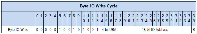
Figure 16 - BUS: KS10 Byte IO Write Cycle
The WRU Cycle is an IO READ bus cycle that to determine which UBA, if any, is currently requesting an interrupt.
WRU Cycles always assert READ (bit 3), negate WRITE (bit 5), assert PHYSICAL (bit 8), assert IO (bit 10), and assert WRU (bit 11).
The address bits (ADDR[18:0]) are ignored and the requested PI Level is asserted onto PI bits (ADDR[15:17]).

Figure 17 - BUS: KS10 WRU Cycle
Vector Cycles always assert READ (bit 3), negate WRITE (bit 5), assert PHYSICAL (bit 8), assert IO (bit 10), and assert VECT (bit 12).
The address bits (ADDR[18:0]) are ignored and the requested UBA number is asserted onto UBA # bits (ADDR[14:17]).

Figure 18 - BUS: KS10 Interrupt Vector Cycle
The interrupt sequence is as follows:
- The IO Device asserts one of the Device Interrupt Request (devINTR[7:4]) signals.
-
The IO Bus Bridge “ORs” the Device Interrupt Request signals (devINTR[7:4]) from each of the IO Devices together.
Next the IO Bus Bridge maps the Device Interrupt Request signals to one of the 7 CPU interrupt request priorities using the High Priority and Low Priority register settings in the IO Bus Bridge Control and Status Register.
Next, the IO Bus Bridge asserts the CPU Interrupt signals onto the busINTR[1:7] pins of the Backplane Bus.
See the Priority Interrupt High (PIH) and the Priority Interrupt Low (PIL) bits of the UBA Status Register (UBACSR) for more information on how this interrupt priority mapping occurs.
- The Backplane Bus Arbiter “ORs” together the External Priority Interrupt signals from each of the IO Bus Bridges and sends the result to the Priority Interrupt Controller inside CPU.
-
The Priority Interrupt Controller inside the CPU selects the highest priority interrupt and interrupts the CPU by asserting the “pageFAIL” signal.
The CPU microcode eventually notices that the “pageFAIL” signal is asserted and dispatches to the interrupt processing microcode.
There, the CPU issues a Who Are You (WRU) bus cycle with the interrupt priority that is being handled.
-
All the IO Bus Bridges receive the WRU bus cycle and each IO Bus Bridge compares the interrupt priority associated with the WRU with the interrupt priority it may be asserting.
If the priority of the WRU bus cycle matches the priority of the IO Bus Bridge, the IO Bus Bridge responds with its WRU identifier response.
- It is possible that more than one IO Bus Bridge is
asserting the same interrupt. If so, the KS10 Backplane
Bus Arbiter selects the highest priority IO Bus Bridge’s
WRU response.
Note: the lowest UBA number is the highest priority IO Bus Bridge. - It is also possible that more than one device attached to the IO Bus Bridge is asserting that same interrupt request. For the purpose of WRU bus cycle, this is irrelevant. This will be resolved later during the Interrupt Vector Cycle.
When this occurs, the microcode in the CPU remembers the UBA number associated with the interrupt.
Note: the WRU identifiers are enumerated in the WIKI section above describing Bus Cycles .
- It is possible that more than one IO Bus Bridge is
asserting the same interrupt. If so, the KS10 Backplane
Bus Arbiter selects the highest priority IO Bus Bridge’s
WRU response.
-
The microcode in the CPU examines the identifier that is received, if any.
If no identifier is received, the CPU handles the interrupt as an APR interrupt.
If an identifier is received, the CPU performs an Interrupt Vector bus cycle which is addressed to the IO Bus Bridge that was associated with the WRU identifier that was arbitrated and received by the CPU.
-
The addressed IO Bus Bridge arbitrates the the Interrupt Vector bus cycle to the highest priority device that is asserting the highest priority interrupt; but note, the interrupt priority selection occurs before the device selection.
The selected device responds with its associated Interrupt Vector and the IO Bridge forwards the Interrupt Vector back to the CPU.
The device uses the Interrupt Vector bus cycle as an Interrupt Acknowledge indication.
Note: as an implementation detail, the timing of the Interrupt Acknowledge with respect to the Interrupt Vector bus cycle is important:
- If the interrupt clears during the Interrupt Vector bus cycle, the interrupt vector will be misread by the microcode.
- If the interrupt clears much after the Interrupt Vector bus cycle is complete, the interrupt will be recognized twice.
Therefore, it is recommend that IO devices acknowledge that the interrupt (clear the interrupt) immediately after the Interrupt Vector bus cycle.
- The CPU software handles the interrupt as described by the KS10 Architecture.
At startup, the Intel Cyclone 5 Arm Cortex-A9 Hard Processor System (HPS) boots Ångström Linux as would any small system. The HPS hardware provides a 32-bit wide memory-mapped AXI4-Lite interface to the FPGA. The KS10 FPGA implements a similarly configured AXI4-Lite slave device which can receive AXI4 communications from the HPS.
Therefore, architecturally, the KS10 is a slave peripheral of the HPS system and all aspects of the KS10 are controlled by the HPS. This design echoes the design of the DEC KS10 where the Console Processor was a much less capable Intel 8080.
Beyond the obvious register interface, the interface should provide two interrupts from the KS10 to the console processor in order to handle asynchronous events.
In this system, The CTY either communicates with the console processor if the KS10 is halted or communicates with the KS10 if the KS10 is running. The best implementation of this has an interrupt that triggers any time that the KS10 run/halt status changes.
Also the characters from the KS10 to the CTY occur asynchronously. A second interrupt that indicates that a character is available would be nice but not mandatory.
For now, neither of these interrupts are present. The console processor creates a thread that polls the RUN/HALT state and polls for a character to be received. It is not the best implementation but it is acceptable.
As noted previously, the KS10 implements a mix of 32-bit, 36-bit, and 64-bit AXI4-Lite slave memory-mapped registers that that the HPS can access. These are:
| Table 3 - CON: KS10 Interface Register Inventory | |||||||||||||||||||
|---|---|---|---|---|---|---|---|---|---|---|---|---|---|---|---|---|---|---|---|
| Address | Width(Bits) | Name | Description | ||||||||||||||||
| 0x00 | 36 | CONAR | Console Address Register | ||||||||||||||||
| 0x08 | 36 | CONDR | Console Data Register | ||||||||||||||||
| 0x10 | 36 | CONIR | Console Instruction Register | ||||||||||||||||
| 0x18 | 32 | CONCSR | Console Control/Status Register | ||||||||||||||||
| 0x1c | 32 | DZCCR | DZ11 Console Control Register | ||||||||||||||||
| 0x20 | 32 | LPCCR | LP20 Console Control Register | ||||||||||||||||
| 0x24 | 32 | RPCCR | RPxx Console Control Register | ||||||||||||||||
| 0x28 | 32 | MTCCR | MT Console Control Register | ||||||||||||||||
| 0x2c | 32 | DUPCCR | DUP11 Console Control Register | ||||||||||||||||
| 0x30 | 32 | KMCCCR | KMC11 Console Control Register (not implemented) | ||||||||||||||||
| 0x34 | 32 | - | Reserved | ||||||||||||||||
| 0x38 | 32 | - | Reserved | ||||||||||||||||
| 0x3c | 32 | - | Reserved | ||||||||||||||||
| 0x40 | 32 | - | Reserved | ||||||||||||||||
| 0x44 | 32 | - | Reserved | ||||||||||||||||
| 0x48 | 32 | - | Reserved | ||||||||||||||||
| 0x4c | 32 | - | Reserved | ||||||||||||||||
| 0x50 | 64 | ITR | Instruction Trace Register | ||||||||||||||||
| 0x58 | 64 | PCIR | PC and IR Registers | ||||||||||||||||
| 0x60 | 64 | MTDIR | MT Data Interface Register | ||||||||||||||||
| 0x68 | 64 | MTDEBUG | MT Debug Register | ||||||||||||||||
| 0x70 | 64 | RPDEBUG | RP Debug Register | ||||||||||||||||
| 0x78 | 32 | - | Reserved | ||||||||||||||||
| 0x7c | 32 | - | Reserved | ||||||||||||||||
| 0x80 | 36 | BRAR[0] | Breakpoint Address Register #0 | ||||||||||||||||
| 0x88 | 36 | BRMR[0] | Breakpoint Mask Register #0 | ||||||||||||||||
| 0x90 | 36 | BRAR[1] | Breakpoint Address Register #1 | ||||||||||||||||
| 0x98 | 36 | BRMR[1] | Breakpoint Mask Register #1 | ||||||||||||||||
| 0xa0 | 36 | BRAR[2] | Breakpoint Address Register #2 | ||||||||||||||||
| 0xa8 | 36 | BRMR[2] | Breakpoint Mask Register #2 | ||||||||||||||||
| 0xb0 | 36 | BRAR[3] | Breakpoint Address Register #3 | ||||||||||||||||
| 0xb8 | 36 | BRMR[3] | Breakpoint Mask Register #3 | ||||||||||||||||
| 0xbc | 32 | - | Reserved | ||||||||||||||||
| 0xc0 | 32 | - | Reserved | ||||||||||||||||
| 0xc4 | 32 | - | Reserved | ||||||||||||||||
| 0xc8 | 32 | - | Reserved | ||||||||||||||||
| 0xcc | 32 | - | Reserved | ||||||||||||||||
| 0xd0 | 32 | - | Reserved | ||||||||||||||||
| 0xd4 | 32 | - | Reserved | ||||||||||||||||
| 0xd8 | 32 | - | Reserved | ||||||||||||||||
| 0xdc | 32 | - | Reserved | ||||||||||||||||
| 0xe0 | 32 | - | Reserved | ||||||||||||||||
| 0xe4 | 32 | - | Reserved | ||||||||||||||||
| 0xe8 | 32 | - | Reserved | ||||||||||||||||
| 0xec | 32 | - | Reserved | ||||||||||||||||
| 0xf0 | 32 | - | Reserved | ||||||||||||||||
| 0xf4 | 32 | - | Reserved | ||||||||||||||||
| 0xf8 | 64 | FVER | Firmware Version Register | ||||||||||||||||
A few of these registers are recognizable to someone familiar with the DEC KS10. Most of them are modern additions that I've found useful enough to implement. These registers will be described in the following sections.
Note: A 64-bit aligned address space is reserved for each of the 36-bit register and each 36-bit register is right justified in that 64-bit address space.
The following sections detail the Console Interface register set.
The address that is used by the KS10 FPGA backplane bus is supplied by the Console Address Register.

Figure 19 - CON: KS10 Console Address Register (CONAR)
LThe address register definition is identical to the backplane bus definition that is described in Section 3.1, i.e., the bits of the Console Address Register are directly applied, 1:1, to the address bus of the backplane. This is illustrated below:

Figure 20 - CON: KS10 Console Address Register (CONAR) Bit Definitions
The Console Data Register is a 36-bit register that provides the data during a console-initiated memory or IO write transaction. The Console Data Register also receives the data that that is read during a console-initiated memory or IO read transaction.
Figure 21 - CON: KS10 Console Data Register (CONDR)
The Console Instruction Register is a 36-bit IO register located at IO Address o200000. After the KS10 Microcode initializes the KS10 micro-machine it fetches the contents of the Console Instruction Register and executes that instruction.
Normally this is a JRST instruction that jumps to the starting address of the boot loader or diagnostic code although the implementation places no constraints on the instruction that placed in this register. A JRST Instruction is opcode o254.
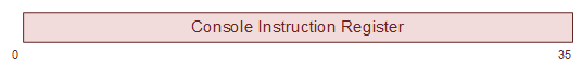
Figure 22 - CON: KS10 Console Instruction Register (CONIR)
The Console Control/Status Register is used to control the KS10 FPGA and to obtain status from the KS10 FPGA.

Figure 23 - CON: KS10 Console Control/Status Register (CONCSR)
| Table 4 - CON: KS10 Console Control/Status Register Definitions | |||||||||||||||||||
|---|---|---|---|---|---|---|---|---|---|---|---|---|---|---|---|---|---|---|---|
| Bit(s) | Mnemonic | R/W | Init | Description | |||||||||||||||
| 0-14 | Reserved | R | - |
Reserved Writes ignored. Always read as zero. |
|||||||||||||||
| 15 | GO/BUSY | R/W | 0 |
GO/Busy When GO is asserted, this bit starts a state-machine that performs a memory or IO transaction. BUSY (read) remains asserted until the memory or IO transaction is completed. When the bus transaction has completed, this bit will be negated automatically. Note: The Console Address Register and Console Data Register should not be modified when this bit is asserted. |
|||||||||||||||
| 16-21 | Reserved | R | - |
Reserved Writes ignored. Always read as zero. |
|||||||||||||||
| 22 | NXM/NXD | R/W | 0 |
Non-existent Memory or Non-existent Device NXM/NXD is asserted if the last console-initiated bus transaction is not acknowledged by a memory or IO device. This bit is reset by writing a zero. |
|||||||||||||||
| 23 | HALT | R | - |
KS10 HALT Status Writes ignored. Halt is not RUN. |
|||||||||||||||
| 24 | RUN | R/W | 0 |
KS10 Run Status When RUN is asserted, the KS10 will begin execution. When the RUN bit is negated, the KS10 will stop execution. The RUN bit is negated automatically by the KS10 microcode when a HALT condition occurs. See the section entitled "Controlling the KS10" for additional information about the RUN bit. |
|||||||||||||||
| 25 | CONT | W | 0 |
KS10 KS10 Continue When CONT is asserted, the KS10 will exit the HALT state execute at least one instruction. The CONT bit is automatically cleared by the KS10 microcode once it is sampled and is always read as zero. See the section entitled "Controlling the KS10" for additional information about the CONT bit. |
|||||||||||||||
| 26 | EXEC | W | 0 |
KS10 Execute When EXEC is asserted, the KS10 will exit the HALT State and execute the instruction in the Console Instruction Register (CONIR). The EXEC bit is automatically cleared by the KS10 microcode once it is sampled and is always read as zero. See the section entitled "Controlling the KS10" for additional information about the EXEC bit. |
|||||||||||||||
| 27 | TIMER EN | R/W | 0 |
Timer Enable This bit enables the KS10 one millisecond interval timer. |
|||||||||||||||
| 28 | TRAP EN | R/W | 0 |
Trap Enable This bit enables KS10 traps. |
|||||||||||||||
| 29 | CACHE EN | R/W | 0 |
Cache Enable This bit enables the KS10 cache. |
|||||||||||||||
| 30 | KS10_INTR | W | 0 |
This bit generates an interrupt from the Console to the KS10. Writing a ‘1’ will generate the interrupt; writing a '0' does nothing. This bit is always read as zero. |
|||||||||||||||
| 31 | KS10_RESET | R/W | 1 |
When KS10_RESET is asserted, the KS10 is held in reset. KS10_RESET asserted (and the KS10 is held in reset) at power-up, otherwise KS10_RESET reflects the last value written. Note: The console microcontroller should initialize the most of the interface registers before negating the KS10_RESET signal. Note also: This does not reset any of the peripherals. |
|||||||||||||||
The DZ11 Modem Control lines are not available external to the KS10 FPGA Board. The DZ11 Console Control Register is used to configure the DZ11 Modem Status register. It also controls the DZ11 loopback.

Figure 24 - CON: DZ11 Console Control Register (DZCCR)
| Table 5 - CON: DZ11 Console Control Register (DZCCR) Definition | |||||||||||||||||||
|---|---|---|---|---|---|---|---|---|---|---|---|---|---|---|---|---|---|---|---|
| Bit(s) | Mnemonic | R/W | Description | ||||||||||||||||
| 0-15 | Reserved | R/W |
Reserved Unused bits are read/write. |
||||||||||||||||
| 16-23 | CO[7:0] | R/W |
Carrier Sense These bits are reflected in the DZ11 Modem Status Register bits 15 through 8. |
||||||||||||||||
| 24-31 | RI[7:0] | R/W |
Ring Indication These bits are reflected in the DZ11 Modem Status Register bits 7 through 0. |
||||||||||||||||
The LP20 Console Control Register controls the interface between the KS10 and the serial printer. It also provides feedback on the number of line per inch and whether the printer is on-line. Lastly the operator can control whether the simulated printer has a optical vertical format unit or a digital (programmable) vertical format unit. It can also set the serial bus parameters to the printer.

Figure 25 - CON: LP Console Control Register (LPCCR)
| Table 6 - CON: LP20 Console Control Register (LPCCR) Definitions | |||||||||||||||||||
|---|---|---|---|---|---|---|---|---|---|---|---|---|---|---|---|---|---|---|---|
| Bit(s) | Mnemonic | R/W | Description | ||||||||||||||||
| 0-5 | - | R/W | Unused. | ||||||||||||||||
| 6-10 | SPEED | R/W | Baud Rate | ||||||||||||||||
| 0 | 50 Baud | ||||||||||||||||||
| 1 | 75 Baud | ||||||||||||||||||
| 2 | 110 Baud | ||||||||||||||||||
| 3 | 134.5 Baud | ||||||||||||||||||
| 4 | 150 Baud | ||||||||||||||||||
| 5 | 300 Baud | ||||||||||||||||||
| 6 | 600 Baud | ||||||||||||||||||
| 7 | 1200 Baud | ||||||||||||||||||
| 8 | 1800 Baud | ||||||||||||||||||
| 9 | 2000 Baud | ||||||||||||||||||
| 10 | 2400 Baud | ||||||||||||||||||
| 11 | 3600 Baud | ||||||||||||||||||
| 12 | 4800 Baud | ||||||||||||||||||
| 13 | 7200 Baud | ||||||||||||||||||
| 14 | 9600 Baud | ||||||||||||||||||
| 15 | 19200 Baud | ||||||||||||||||||
| 16 | 38400 Baud | ||||||||||||||||||
| 17 | 57600 Baud | ||||||||||||||||||
| 18 | 115200 Baud | ||||||||||||||||||
| 19 | 230400 Baud | ||||||||||||||||||
| 20 | 460800 Baud | ||||||||||||||||||
| 21 | 921600 Baud | ||||||||||||||||||
| 22-31 | Reserved | ||||||||||||||||||
| 11-12 | LENGTH | R/W | Number of Bits | ||||||||||||||||
| 0 | 5 Bits | ||||||||||||||||||
| 1 | 6 Bits | ||||||||||||||||||
| 2 | 7 Bits | ||||||||||||||||||
| 3 | 8 Bits | ||||||||||||||||||
| 13-14 | PARITY | R/W | Parity Type | ||||||||||||||||
| 0 | No Parity | ||||||||||||||||||
| 1 | Odd Parity | ||||||||||||||||||
| 2 | Even Parity | ||||||||||||||||||
| 3 | Mark Parity | ||||||||||||||||||
| 15 | STOPS | R/W | Number of Stop Bits | ||||||||||||||||
| 0 | 1 Stop Bit | ||||||||||||||||||
| 1 | 2 Stop Bits | ||||||||||||||||||
| 16-28 | - | R | Reserved | ||||||||||||||||
| 29 | SIXLPI | R | LPI | ||||||||||||||||
| 0 | 8 LPI | ||||||||||||||||||
| 1 | 6 LPI | ||||||||||||||||||
| 30 | OVFU | R/W | Vertical Formatting Unit | ||||||||||||||||
| 0 | Digital Vertical Format Unit | ||||||||||||||||||
| 1 | Optical Vertical Format Unit/p> | ||||||||||||||||||
| 31 | ONLINE | R/W | Printer State | ||||||||||||||||
| 0 | Printer Of-line | ||||||||||||||||||
| 1 | Printer On-line | ||||||||||||||||||
The Magtape Console Control Register controls the status of the various TU-45 tape drives. Normally, these controls would be present on the tape drive but need to be emulated in this application.
Note: The format of this register is very similar to the RPCCR; but there are a few differences. The KS10 FPGA supports only a single TM03 Tape Control Unit (TCU), or formatter, which is Unit 0. The single TCU can support 8 slave drives.

Figure 26 - CON: MT Console Control Register (MTCCR)
| Table 7 - CON: MT Console Control Register (MTCCR) | |||||||||||||||||||
|---|---|---|---|---|---|---|---|---|---|---|---|---|---|---|---|---|---|---|---|
| Bit(s) | Mnemonic | R/W | Description | ||||||||||||||||
| 0-7 | - | R/W |
Reserved Unused. |
||||||||||||||||
| 8 | DPR[7] | R/W | Drive 7 Present | ||||||||||||||||
| 9 | DPR[6] | R/W | Drive 6 Present | ||||||||||||||||
| 10 | DPR[5] | R/W | Drive 5 Present | ||||||||||||||||
| 11 | DPR[4] | R/W | Drive 4 Present | ||||||||||||||||
| 12 | DPR[3] | R/W | Drive 3 Present | ||||||||||||||||
| 13 | DPR[2] | R/W | Drive 2 Present | ||||||||||||||||
| 14 | DPR[1] | R/W | Drive 1 Present | ||||||||||||||||
| 15 | DPR[0] | R/W | Drive 0 Present | ||||||||||||||||
| 16 | MOL[7] | R/W | Drive 7 Media On-line | ||||||||||||||||
| 17 | MOL[6] | R/W | Drive 6 Media On-line | ||||||||||||||||
| 18 | MOL[5] | R/W | Drive 5 Media On-line | ||||||||||||||||
| 19 | MOL[4] | R/W | Drive 4 Media On-line | ||||||||||||||||
| 20 | MOL[3] | R/W | Drive 3 Media On-line | ||||||||||||||||
| 21 | MOL[2] | R/W | Drive 2 Media On-line | ||||||||||||||||
| 22 | MOL[1] | R/W | Drive 1 Media On-line | ||||||||||||||||
| 23 | MOL[0] | R/W | Drive 0 Media On-line | ||||||||||||||||
| 24 | WRL[7] | R/W | Drive 7 Write Locked | ||||||||||||||||
| 25 | WRL[6] | R/W | Drive 6 Write Locked | ||||||||||||||||
| 26 | WRL[5] | R/W | Drive 5 Write Locked | ||||||||||||||||
| 27 | WRL[4] | R/W | Drive 4 Write Locked | ||||||||||||||||
| 28 | WRL[3] | R/W | Drive 3 Write Locked | ||||||||||||||||
| 29 | WRL[2] | R/W | Drive 2 Write Locked | ||||||||||||||||
| 30 | WRL[1] | R/W | Drive 1 Write Locked | ||||||||||||||||
| 31 | WRL[0] | R/W | Drive 0 Write Locked | ||||||||||||||||
The RP Console Control Register controls the status of the various RP06 disk drives. Real RP06 disk drives provided controls are not emulated in the FPGA because of the SDHC media. These are:

Figure 27 - CON: RP Console Control Register (RPCCR)
| Table 8 - CON: RP Console Control Register (RPCCR) | |||||||||||||||||||
|---|---|---|---|---|---|---|---|---|---|---|---|---|---|---|---|---|---|---|---|
| Bit(s) | Mnemonic | R/W | Description | ||||||||||||||||
| 0-7 | - | R/W |
Reserved Unused. |
||||||||||||||||
| 8 | DPR[7] | R/W | Drive 7 Present | ||||||||||||||||
| 9 | DPR[6] | R/W | Drive 6 Present | ||||||||||||||||
| 10 | DPR[5] | R/W | Drive 5 Present | ||||||||||||||||
| 11 | DPR[4] | R/W | Drive 4 Present | ||||||||||||||||
| 12 | DPR[3] | R/W | Drive 3 Present | ||||||||||||||||
| 13 | DPR[2] | R/W | Drive 2 Present | ||||||||||||||||
| 14 | DPR[1] | R/W | Drive 1 Present | ||||||||||||||||
| 15 | DPR[0] | R/W | Drive 0 Present | ||||||||||||||||
| 16 | MOL[7] | R/W | Drive 7 Media On-line | ||||||||||||||||
| 17 | MOL[6] | R/W | Drive 6 Media On-line | ||||||||||||||||
| 18 | MOL[5] | R/W | Drive 5 Media On-line | ||||||||||||||||
| 19 | MOL[4] | R/W | Drive 4 Media On-line | ||||||||||||||||
| 20 | MOL[3] | R/W | Drive 3 Media On-line | ||||||||||||||||
| 21 | MOL[2] | R/W | Drive 2 Media On-line | ||||||||||||||||
| 22 | MOL[1] | R/W | Drive 1 Media On-line | ||||||||||||||||
| 23 | MOL[0] | R/W | Drive 0 Media On-line | ||||||||||||||||
| 24 | WRL[7] | R/W | Drive 7 Write Locked | ||||||||||||||||
| 25 | WRL[6] | R/W | Drive 6 Write Locked | ||||||||||||||||
| 26 | WRL[5] | R/W | Drive 5 Write Locked | ||||||||||||||||
| 27 | WRL[4] | R/W | Drive 4 Write Locked | ||||||||||||||||
| 28 | WRL[3] | R/W | Drive 3 Write Locked | ||||||||||||||||
| 29 | WRL[2] | R/W | Drive 2 Write Locked | ||||||||||||||||
| 30 | WRL[1] | R/W | Drive 1 Write Locked | ||||||||||||||||
| 31 | WRL[0] | R/W | Drive 0 Write Locked | ||||||||||||||||

Figure 28 - CON: DUP11 Console Control Register (DUPCCR)
| Table 9 - CON: DUP11 Console Control Register (DUPCCR) Definition | |||||||||||||||||||
|---|---|---|---|---|---|---|---|---|---|---|---|---|---|---|---|---|---|---|---|
| Bit(s) | Mnemonic | R/W | Description | ||||||||||||||||
| 0 | Reserved | R/W |
Reserved Unused bits are read/write |
||||||||||||||||
| 1 | TXE | R | Transmitter FIFO empty | ||||||||||||||||
| 2-3 | - | R/W |
Reserved Unused bits are read/write. |
||||||||||||||||
| 4 | RI | R/W | Ring indication | ||||||||||||||||
| 5 | CTS | R/W | Clear to Send | ||||||||||||||||
| 6 | DSR | R/W | Data Set Ready | ||||||||||||||||
| 7 | DCD | R/W | Data Carrier Detect | ||||||||||||||||
| 8-15 | TXFIFO | R | Transmitter FIFO | ||||||||||||||||
| 16 | RXF | R | Receiver FIFO Full | ||||||||||||||||
| 17 | DTR | R | Data terminal ready | ||||||||||||||||
| 18 | RTS | R | Request to send | ||||||||||||||||
| 20 | H325 | R/W | Install H325 Loopback Plug | ||||||||||||||||
| 21 | W3 | R/W | Install W3 Jumper Plug | ||||||||||||||||
| 22 | W5 | R/W | Install W5 Jumper Plug | ||||||||||||||||
| 23 | W6 | R/W | Install W6 Jumper Plug | ||||||||||||||||
| 24-31 | RXFIFO | R/W | RXFIFO Interface | ||||||||||||||||
The Breakpoint Facility monitors the address on the KS10 Backplane Bus and halts the KS10 CPU when the “Address Match” conditions are met.
The Breakpoint Address Register are a set of 36-bit registers that sets the breakpoint address. The Breakpoint Mask Register is another set of 36-bit registers that controls which bits of the Breakpoint Address are used in the breakpoint comparison and which bits are ignored.
It should be noted that the Breakpoint Register examines the KS10 Backplane and therefore operates on Physical Addresses and not on Virtual Addresses. Also, the breakpoint facility will only breakpoint on addresses generated by the CPU. It will not breakpoint on DMA operations.
In actual implmentation, there are 4 sets of breakpoint registers, BRAR[0:3] and BRMR[0:3]. BRAR[0] and BRMR[0] are paired together. Likewise, BRAR[1] and BRMR[1] are paired together, etc.
Because the KS10 backplane implementation has both a READ bit and a WRITE bit associated with the address, a naive breakpoint implementation could not break on either reads or writes - it could only breakpoint on reads and breakpoint on writes. The KS10 FPGA actually implements two address comparisons for each breakpoint register: one address comparison for reads and one address comparison for writes. Therefore for this implementation allows breakpoint on reads or breakpoint on writes.
It goes without saying that there are a lot of bus-cycles that could be detected with the breakpoint system that are not really useful.
The Breakpoint Address Register is illustrated below:

Figure 29 - CON: KS10 Breakpoint Address Register (BRAR[0:3])
The bit definitions of the Breakpoint Address Register Definition are illustrated below:
| Table 10 - CON: KS10 Breakpoint Address Register (BRAR[0:3]) Definitions | |||||||||||||||||||
|---|---|---|---|---|---|---|---|---|---|---|---|---|---|---|---|---|---|---|---|
| Bit(s) | Mnemonic | R/W | Description | ||||||||||||||||
| 0-13 | FLAGS | R/W | Flags | ||||||||||||||||
| 0 | User Mode | ||||||||||||||||||
| 1 | Not used | ||||||||||||||||||
| 2 | Fetch Cycle | ||||||||||||||||||
| 3 | Read Cycle | ||||||||||||||||||
| 4 | Write Test Cycle | ||||||||||||||||||
| 5 | Write Cycle | ||||||||||||||||||
| 6 | Extended Cycle | ||||||||||||||||||
| 7 | Cache Enabled | ||||||||||||||||||
| 8 | Physical Address | ||||||||||||||||||
| 9 | PCXT | ||||||||||||||||||
| 10 | IO Cycle | ||||||||||||||||||
| 11 | IO Who Are You Cycle | ||||||||||||||||||
| 12 | IO Interrupt Cycle | ||||||||||||||||||
| 13 | IO Byte Cycle | ||||||||||||||||||
| 14-35 | ADDRESS | R/W | Address | ||||||||||||||||
The Breakpoint Mask Register(s) (BRMR) provides a mechanism to include or ignore the various address and flag bits that are associated with the Backplane. When a bit is asserted in the BRMR, the associated bit in the Breakpoint Address Register (BRAR) will be included in the breakpoint comparison. When the bit is negated in the BRMR, the bit will be ignored in the breakpoint comparison.
Note: If the READ bit in the BRMR is set, the breakpoint system will breakpoint only on reads. If the WRITE bit in the BRMR is set, the breakpoint system wil l breakpoint on only writes. If both the READ and WRITE bits in the BRMR are both set, the breakpoint will trigger on either reads or writes.
The Breakpoint Mask Register (BRMR[0:3])is illustrated below:

Figure 30 - CON: KS10 Breakpoint Mask Register (BRMR[0:3])
The bit definitions of the Breakpoint Mask Register (BRMR[0:3]) Definition is illustrated below:
| Table 11 - CON: KS10 Breakpoint Mask Register (BRMR[0:3]) Definitions | |||||||||||||||||||
|---|---|---|---|---|---|---|---|---|---|---|---|---|---|---|---|---|---|---|---|
| Bit(s) | Mnemonic | R/W | Description | ||||||||||||||||
| 0-13 | FLAGS | R/W | Flags | ||||||||||||||||
| 0 | User Mode | ||||||||||||||||||
| 1 | Not used | ||||||||||||||||||
| 2 | Fetch Cycle | ||||||||||||||||||
| 3 | Read Cycle | ||||||||||||||||||
| 4 | Write Test Cycle | ||||||||||||||||||
| 5 | Write Cycle | ||||||||||||||||||
| 6 | Extended Cycle | ||||||||||||||||||
| 7 | Cache Enabled | ||||||||||||||||||
| 8 | Physical Address | ||||||||||||||||||
| 9 | PCXT | ||||||||||||||||||
| 10 | IO Cycle | ||||||||||||||||||
| 11 | IO Who Are You Cycle | ||||||||||||||||||
| 12 | IO Interrupt Cycle | ||||||||||||||||||
| 13 | IO Byte Cycle | ||||||||||||||||||
| 14-35 | ADDRESS | R/W | Address | ||||||||||||||||
The Instruction Trace Register allows certain CPU registers to be stored as program execution occurs. As the program executes, the Program Counter (PC) and the Instruction Register (IR) is stored in the Trace Buffer when an instruction is executed.
The Trace Buffer is a simple stack. When the most significant word (bits 0-15) of the Instruction Trace Register is read, the buffer state is updated.
The Instruction Trace Register is defined below:

Figure 31 - CON: KS10 Instruction Trace Register (ITR)
| Table 12 - CON: KS10 Instruction Trace Register (ITR) Definitions | |||||||||||||||||||
|---|---|---|---|---|---|---|---|---|---|---|---|---|---|---|---|---|---|---|---|
| Bit(s) | Mnemonic | R/W | Description | ||||||||||||||||
| 0 | CLR | W |
Clear Asserting CLR will reset the trace buffer. When this occurs, FULL is negated and EMPTY is asserted. Always read as zero. |
||||||||||||||||
| 1 | FULL | R |
Buffer Full Full is asserted when the buffer is full. Full is negated by asserting CLR. Writes ignored. |
||||||||||||||||
| 2 | EMPTY | R |
Buffer Empty Empty is asserted when the buffer is empty. Empty is asserted by asserting CLR. Writes ignored. |
||||||||||||||||
| 3-7 | SIZE[4:0] | R |
Buffer Size The trace buffer size is parameterized. The buffer size is fixed when the FPGA is built. This field reports the actual log2(buffer_size) as implemented in the FPGA. In other words, if the trace buffer size is 4096 entries, this field reports 12. |
||||||||||||||||
| 8-9 | - | R |
Reserved Writes ignored. Always read as zero. |
||||||||||||||||
| 10-27 | PC[18:35] | R |
Program Counter Writes ignored. The PC register contains the captured value Program Counter. |
||||||||||||||||
| 28-63 | IR[0:35] | R |
Instruction Register Writes ignored. The IR register contains the captured value of the Instruction Register. |
||||||||||||||||
Sometimes it's nice just to know what is happening and what code is executing. Typing a ^T on the CTY when the KS10 is executing will capture the PCIR register and print the captured, disassembled instruction on the CTY.
The Program Counter and Instruction Register is defined below:
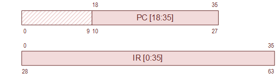
Figure 32 - CON: KS10 Program Counter and Instruction Register (PCIR)
| Table 13 - CON: KS10 Program Counter and Instruction Register (PCIR) Definitions | |||||||||||||||||||
|---|---|---|---|---|---|---|---|---|---|---|---|---|---|---|---|---|---|---|---|
| Bit(s) | Mnemonic | R/W | Description | ||||||||||||||||
| 0-9 | - | R/W |
Reserved Writes ignored. Always read as zero. |
||||||||||||||||
| 10-27 | PC[18:35] | R |
Program Counter Writes ignored. The PC register is loaded with the last value of the Program Counter. |
||||||||||||||||
| 28-63 | IR[0:35] | R |
Instruction Register The IR register is loaded with the last value of the Instruction Register. |
||||||||||||||||
This register is the interface between the Console Processor and the MT Tape Controller.
| Table 14 - CON: MT Data Interface Register (MTDIR) | |||||||||||||||||||
|---|---|---|---|---|---|---|---|---|---|---|---|---|---|---|---|---|---|---|---|
| Bit(s) | Mnemonic | R/W | Description | ||||||||||||||||
| 63 | READ | R |
Tape Read Mode READ is deprecated and should be ignored. |
||||||||||||||||
| 62 | STB | R/W |
Strobe During read functions, the console processor will provide tape data from a file to the Tape Controller by asserting data onto the DATA bits and then asserting STB. Alternately STB and DATA can be asserted simultaneously in a single atomic 64-bit write operation, if that can be guaranteed. In this case, the Tape Controller automatically negates the STB signal once the data has been read. In read mode, the console processor cannot negate the STB signal once asserted. Note: Read functions include Read Forward, Read Reverse, Write Check Forward, and Write Check Reverse. During write functions, the Tape Controller will provide data to the console processor to write to a file, by asserting STB and asserting data on the DATA bits. When the console processor has read the data it should negate the STB signal. DATA should be ignored if STB is negated. In write mode, The console processor cannot assert STB. Note: The only write function is Write Forward. |
||||||||||||||||
| 61 | INIT | R |
Initialize INIT is deprecated and should be ignored. |
||||||||||||||||
| 60 | READY | R/W |
Ready The Tape Controller in the FPGA negates the READY bit to notify the console software to process a command. When the console software has completed the command, it asserts READY. Note: the console processor can only assert the READY bit. It cannot negate the READY bit. The MTDS[DRY] bit reflects the state of this bit. The MTCS1[GO] bit reflects the negated state of this bit. |
||||||||||||||||
| 59 | INCFC | W |
Increment Frame Counter The console processor should assert INCFC to notify the tape controller to increment the Frame Counter. The tape controller automatically negates the INCFC bit when the Frame Counter has been incremented. Negating the INCFC bit has no effect. Always read as zero. |
||||||||||||||||
| 58-56 | SS[2:0] | R |
Slave select Writes ignored. SS reflects the contents of the MTTC[SS] register. |
||||||||||||||||
| 55-53 | DEN[2:0] | R |
Density Writes ignored. DEN reflects the contents of the MTTC[DEN] register. |
||||||||||||||||
| 52-48 | FUN[4:0] | R |
Function Writes ignored. FUN reflects the contents of the MTCS1[FUN] register. |
||||||||||||||||
| 47-44 | FMT[3:0] | R |
Format Writes ignored. FMT reflects the contents of the MTTC[FMT] register. |
||||||||||||||||
| 43 | WCZ | R |
Word Count is Zero Writes ignored. WCZ is asserted when the contents of the Word Count Register is zero. |
||||||||||||||||
| 42 | FCZ | W |
Frame Count is Zero Writes ignored. FCZ is asserted when the contents of the Frame Count Register is zero. |
||||||||||||||||
| 41 | SETBOT | W |
Set Beginning-of-Tape When SETBOT is asserted, the Beginning-of-Tape indication (MTDS[BOT]) will be asserted. Negating the SETBOT bit has no effect. Always read as zero. |
||||||||||||||||
| 40 | CLRBOT | W |
Clear Beginning-of-Tape When CLRBOT is asserted, the Beginning-of-Tape indication (MTDS[BOT]) will be negated. Negating the CLRBOT bit has no effect. Always read as zero. |
||||||||||||||||
| 39 | SETEOT | W |
Set End-of-Tape When SETEOT is asserted, the End-of-Tape indication (MTDS[EOT]) will be asserted. Negating the SETEOT bit has no effect. Always read as zero. |
||||||||||||||||
| 38 | CLREOT | W |
Clear End-of-Tape When CLREOT is asserted, the End-of-Tape indication (MTDS[EOT]) will be negated. Negating the CLREOT bit has no effect. Always read as zero. |
||||||||||||||||
| 37 | SETTM | W |
Set Tape Mark When SETTM is asserted, the Tape Mark indication (MTDS[TM]) will be asserted. Negating the SETTM bit has no effect. Always read as zero. |
||||||||||||||||
| 36 | CLRTM | W |
Clear Tape Mark When CLRTM is asserted, the Tape Mark indication (MTDS[TM]) will be negated. Negating the CLRTM bit has no effect. Always read as zero. |
||||||||||||||||
| 35-0 | DATA[0:35] | R/W |
Tape Data See operation of the STB bit above for a description of how to read and write to the DATA bits. During read operations, DATA is write-only. During write operations, DATA is read-only. The console processor performs all of the tape formatting which involves translating bytes on the tape into 36-bit PDP-10 words and vice-versa. The console processor supports the same formats that the DEC TM03 supports. Note: There is an endian swap in this register. |
||||||||||||||||
The MT Debug Register is a register that is not present on a DEC KS10. It is present only to facilitate debugging the KS10 FPGA MT Tape Controller.

Figure 33 - CON: MT Debug Register (MTDEBUG)
The bit definitions of the MT Debug Register is defined below.
| Table 15 - CON: MT Debug Register (MTDEBUG) Definitions | |||||||||||||||||||
|---|---|---|---|---|---|---|---|---|---|---|---|---|---|---|---|---|---|---|---|
| Bit(s) | Mnemonic | R/W | Description | ||||||||||||||||
| 0-7 | STATE | R |
Tape Controller State Machine State STATE contains the current state of the Tape Controller State Machine. |
||||||||||||||||
| 8-15 | - | R | Reserved | ||||||||||||||||
| 16-23 | - | R | Reserved | ||||||||||||||||
| 24-31 | - | R | Reserved | ||||||||||||||||
| 32-47 | WRCNT | R |
Number of Tape Writes This is a 16-bit counter that is incremented on each write operation. |
||||||||||||||||
| 48-63 | RDCNT | R |
Number of Tape Reads This is a 16-bit counter that is incremented on each read operation. |
||||||||||||||||
The RP Debug Register is a register that is not present on a DEC KS10. It ispresent only to facilitate debugging the KS10 FPGA RP Disk Controller. The FPGA design makes it difficult to probe inside the RP06 controllers to get status. This register also provides Disk Drive blinking lights.

Figure 34 - CON: RP Debug Register (RPDEBUG)
The bit definitions of the RP Debug Register is defined below.
| Table 16 - CON: RP Debug Register (RPDEBUG) Definitions | |||||||||||||||||||
|---|---|---|---|---|---|---|---|---|---|---|---|---|---|---|---|---|---|---|---|
| Bit(s) | Mnemonic | R/W | Description | ||||||||||||||||
| 0-7 | STATE | R |
SDHC Card State Machine State STATE contains the current state of the State Machine that manages the interface to the SD Card. |
||||||||||||||||
| 8-15 | ERRNUM | R |
Error Number When the State Machine detects an issue with the SD Card interface, the State Machine records ERRNUM which uniquely describes the circumstances of the failure. |
||||||||||||||||
| 16-23 | ERRVAL | R |
Error Value When the State Machine detects an unexpected or incorrect response from the SD Card, the State Machine records response of the SD Card in ERRVAL. |
||||||||||||||||
| 24 | DISK0 | R | Disk 0 Activity LED | ||||||||||||||||
| 25 | DISK1 | R | Disk 1 Activity LED | ||||||||||||||||
| 26 | DISK2 | R | Disk 2 Activity LED | ||||||||||||||||
| 27 | DISK3 | R | Disk 3 Activity LED | ||||||||||||||||
| 28 | DISK4 | R | Disk 4 Activity LED | ||||||||||||||||
| 29 | DISK5 | R | Disk 5 Activity LED | ||||||||||||||||
| 30 | DISK6 | R | Disk 6 Activity LED | ||||||||||||||||
| 31 | DISK7 | R | Disk 7 Activity LED | ||||||||||||||||
| 32-47 | WRCNT | R |
Number of Disk Writes This is a 16-bit counter that is incremented on each write operation. |
||||||||||||||||
| 48-63 | RDCNT | R |
Number of Disk Reads This is a 16-bit counter that is incremented on each read operation. |
||||||||||||||||
The Firmware Version Register is used for basic diagnostics and to allow the console to print the firmware revision of the FPGA.
One of the first tests that the console will perform is to attempt to read the contents of the Firmware Version Register from the FPGA. If the result is not consistent with the expected results, the console will print an error message and not attempt to boot the KS10 processor.
This test verifies that the FPGA is programmed and that there is a working bus connection between the console microcontroller and the FPGA.
The format of the Firmware Version Register is summarized below.

Figure 35 - CON: KS10 Firmware Version Register (FVR)
The bit definitions of the Firmware Version Register is defined below.
| Table 17 - CON: KS10 Firmware Version Register (FVR) Definitions | |||||||||||||||||||
|---|---|---|---|---|---|---|---|---|---|---|---|---|---|---|---|---|---|---|---|
| Byte | Value | ASCII | R/W | Description | |||||||||||||||
| 0 | 0x52 | 'R' | R | Always 'R' | |||||||||||||||
| 1 | 0x45 | 'E' | R | Always 'E' | |||||||||||||||
| 2 | 0x56 | 'V' | R | Always 'V' | |||||||||||||||
| 3 | * | * | R | Major Revision MS Byte | |||||||||||||||
| 4 | * | * | R | Major Revision LS Byte | |||||||||||||||
| 5 | 0x2e | '.' | R | Always '.' | |||||||||||||||
| 6 | * | * | R | Minor Revision MS Byte | |||||||||||||||
| 7 | * | * | R | Minor Revision LS Byte | |||||||||||||||
|
* Contents depend of firmware revision which is built into the firmware. When printed, the firmware version register looks something like "REV23.45" |
|||||||||||||||||||
This section describes the signals that are generated by the Console Microcontroller that control the operation of the KS10.
The RUN bit, the CONT bit, and the
EXEC bit control the KS10 operation as illustrated below:

Figure 36 - CON: KS10 Control State Diagram
When in the HALT State, the table below enumerates the
types of operations that the KS10 will perform when the control bits
are set in the various states.
| Table 18 - CON: KS10 Control Interface | |||||||||||||||||||
|---|---|---|---|---|---|---|---|---|---|---|---|---|---|---|---|---|---|---|---|
| CONT | EXEC | RUN | Operation | ||||||||||||||||
| 0 | X | X | Remain in HALT State. | ||||||||||||||||
| 1 | 0 | 0 | Execute the single instruction at current PC (i.e., single step). | ||||||||||||||||
| 1 | 0 | 1 | Continue execution at current PC. | ||||||||||||||||
| 1 | 1 | 0 | Execute the single instruction in the Console Instruction Register. | ||||||||||||||||
| 1 | 1 | 1 | Begin execution with the instruction in the Console Instruction Register. | ||||||||||||||||
The operation of these bits is also detailed in the following sections.
The RUN bit controls whether the KS10 is in the
RUN State or HALT State.
Setting the RUN bit will allow the KS10 to execute one or
more instructions.
The RUN bit is examined by the microcode at the end of each instruction.
When the RUN bit is asserted, the KS10 will execute the
next instruction.
When the RUN bit is cleared, the KS10 will finish the
current instruction and enter the Halt State.
When the KS10 is in the HALT State, setting the
CONT bit will cause the KS10 to exit the
HALT State and execute at least one instruction.
At the end of that instruction, the RUN bit is examined.
If the RUN bit is asserted, the KS10 will continue
to execute instructions.
If the RUN bit is negated, the KS10 will re-enter the
HALT State - essentially single-stepping the processor.
When the KS10 is in the HALT State, setting the
CONT bit and EXEC bit will cause the
KS10 to exit the HALT State and execute the
instruction in the Console Instruction Register (CIR).
At the end of that instruction, the RUN bit is
examined.
If the RUN bit is asserted, the KS10 will continue
to execute instructions.
This technique is used by the Console at startup to cause the KS10
to begin executing the boot loader or diagnostic program at a specific
address.
In this case, a JRST instruction which performs a jump to the starting
address of the boot loader is placed into the Console Instruction Register.
If the RUN bit is negated, the KS10 will re-enter the
HALT State - essentially executing the single instruction
in the Console Instruction Register (CIR).
The Console Communications Area is a region of KS10 memory that is accessible by both the KS10 and the Console Processor. This memory is used to communicate between the two devices.
Most of the information in this section is not very well documented. It has mostly been obtained by reading the monitor source code and reading the I8080 "microcode".
| Table 19 - CON: KS10 Console Communications Area | |||||||||||||||||||
|---|---|---|---|---|---|---|---|---|---|---|---|---|---|---|---|---|---|---|---|
| Address | Value | Summary | |||||||||||||||||
| 000030 | 000000_000000 |
The Halt Switch memory location is used by the console processor to shutdown or restart the monitor program. |
|||||||||||||||||
| 000031 | 003740_000000 |
The Keep Alive memory location is used by the console processor to periodically check the status of the monitor program executing in the KS10 and take action (reboot) if necessary. The console processor can also interact with the monitor program at startup so that the reason for the reboot is captured in the log files. |
|||||||||||||||||
| 000032 |
This memory location contains the CTY Input Word. This is used to send characters from the console processor to the KS10. |
||||||||||||||||||
| 000033 |
This memory location contains the CTY Output Word. This is used by the KS10 to send characters to the console processor. |
||||||||||||||||||
| 000034 |
KLINIK Input Word. KLINIK is not implemented. |
||||||||||||||||||
| 000035 |
KLINIK Output Word. KLINIK is not implemented. |
||||||||||||||||||
| 000036 |
RP Disk: 1776700 MT Tape: 3772440 |
This memory location contains to address of the RH11 Massbus Controller for the boot device. The RH11 address includes the UBA number. |
|||||||||||||||||
| 000037 |
This memory location contains the unit number of the boot device. |
||||||||||||||||||
| 000040 | 000000_002000 |
This memory location contains the magtape parameters of the boot device. The contents of this memory location is used to set the MT Tape Control Register (MTTC) if the boot device is a magtape. If the boot device is a disk drive, this parameter is ignored. |
|||||||||||||||||
| Table 20 - CON: KS10 Halt Switch (KS10 Memory Address 000030) | |||||||||||||||||||
|---|---|---|---|---|---|---|---|---|---|---|---|---|---|---|---|---|---|---|---|
| Bit(s) | Mnemonic | Description | |||||||||||||||||
| 0-35 | HALT |
Halt Switch This register is initialized to zero at startup. The console processor can request that the monitor shut itself down by storing a non-zero value to this location. If the value written is the base address of the RH11 disk controller (01776700) the monitor will reboot. |
|||||||||||||||||
The Keep Alive Word bits-fields are aligned on bytes because of the i8080 interface. The i8080 has a 32-bit interface to this 36-bit memory location. The bits are organized into bytes as follows:
- Bits 0-3 are not accessed by the i8080.
- Bits 4-11 (Byte 0) are configuration bits.
- Bits 12-19 (Byte 1) are also configuration bits.
- Bits 20-27 (Byte 2) is the keep alive byte.
- Bits 28-35 (Byte 3) are the "Why reload?" bits.
| Table 21 - CON: KS10 Keep Alive Word (KS10 Memory Address 000031) | |||||||||||||||||||
|---|---|---|---|---|---|---|---|---|---|---|---|---|---|---|---|---|---|---|---|
| Bit(s) | Mnemonic | Byte | Description | ||||||||||||||||
| 0-3 | - | - | This part of the Keep Alive Word is not accessible by the 8080 and is not used. | ||||||||||||||||
| 4 | KSRLD |
Byte 0 Configuration |
Reload Request The KS10 asserts this bit to ask the console processor to reload the KS10. When this occurs, the console processor will:
|
||||||||||||||||
| 5 | KPACT |
Keep Alive Active The console processor will reload the KS10 if this is asserted and KPALIV does not change. The KS10 increments the KPALIV field every second and the console processor periodically checks the KPALIV bits. If the console processor does not detect a change in the KPALIV field after 15 seconds, the console processor will reboot the KS10. When this occurs, the console processor will:
|
|||||||||||||||||
| 6 | KLACT |
KLINIK Active KLINIK is not implemented. |
|||||||||||||||||
| 7 | PAREN |
Memory Parity Error Detect Enabled The console processor normally sets PAREN at startup. The KS10 FPGA doesn't implement parity so this has no effect. |
|||||||||||||||||
| 8 | CRMPAR |
CRAM Parity Error Detect Enabled The console processor normally sets CRMPAR at startup. The KS10 FPGA doesn't implement parity so this has no effect. |
|||||||||||||||||
| 9 | DRMPAR |
DRAM Parity Error Detect Enabled The console processor normally sets DRMPAR at startup. The KS10 FPGA doesn't implement parity so this has no effect. |
|||||||||||||||||
| 10 | CASHEN |
Cache Enabled The console processor normally sets CASHEN at startup. |
|||||||||||||||||
| 11 | MILSEN |
1 Millisecond Timer Enabled The console processor normally sets MILSEN at startup. |
|||||||||||||||||
| 12 | TRPENA |
Byte 1 Configuration |
Traps Enabled The console processor normally sets TRPENA at startup. |
||||||||||||||||
| 13 | MFGMOD |
Manufacturing Mode The console processor always sets this to zero. |
|||||||||||||||||
| 14-19 | - |
Reserved Reserved bits should be set to zero. |
|||||||||||||||||
| 20-27 | KPALIV |
Byte 2 Keep alive byte |
Keep Alive When operating properly, the KS10 increments KPALIV every second. See description of KPACT above for more information. |
||||||||||||||||
| 28-32 | - |
Byte 3 Why reload? |
Reserved Reserved bits should be set to zero. |
||||||||||||||||
| 32 | AUTOBT |
Auto boot AUTOBT is asserted by the console processor at startup or when the boot switch is activated. The monitor uses this bit to log why the startup is occurring. |
|||||||||||||||||
| 33 | PWRFAL |
Power Fail Restart PWRFAL is asserted by the console processor before a startup that was caused by a power failure. The monitor uses this bit to log why the startup is occurring. The KS10 FPGA doesn't implement power fail. It looks like the KS10 didn't support power fail either. The comments for the Version 5.2 I8080 microcode states: (5.2G) THIS CODE WAS FOR HANDLING POWER FAIL RESTART WITH BATTERY BACKUP. SINCE THERE IS NO BATTERY BACKUP ANY MORE, IT IS TAKEN OUT. |
|||||||||||||||||
| 34 | FORREL |
Forced Reload FORREL is asserted by the console processor before a startup that was caused by a reload request. The monitor uses this bit to log why the startup is occurring. The misnomer "Forced Reload" is inconsistently applied to this bit. |
|||||||||||||||||
| 35 | KEPFAL |
Keep alive failure KEPFAL is asserted by the console processor before a startup that was caused by a keep-alive failure. The monitor uses this bit to log why the startup is occurring. |
|||||||||||||||||
The CTY input protocol uses KS10 memory location 000032 to transfer the CTY character plus a 1-bit flag (Valid) from the Console Processor to the KS10.
This is illustrated below:

Figure 37 - CON: KS10 CTY Input Word (KS10 Memory Address 000032)
| Table 22 - CON: KS10 CTY Output Word (KS10 Memory Address 000032) | |||||||||||||||||||
|---|---|---|---|---|---|---|---|---|---|---|---|---|---|---|---|---|---|---|---|
| Bit(s) | Mnemonic | Description | |||||||||||||||||
| 0-26 | Reserved | Ignored for reads and writes. | |||||||||||||||||
| 27 | VALID |
Asserted by Console Processor when character is available for the KS10 to read. Cleared by the KS10 after the character has been read. |
|||||||||||||||||
| 28-35 | CTY Character |
ASCII Character. Asserted by Console Processor when character is available for the KS10 to read. Cleared by the KS10 after the character has been read. |
|||||||||||||||||
The procedure from transferring a character from the Console Processor to the KS10 is as follows:
- The Console Processor verifies that there is no character already in the buffer to the KS10 by checking the VALID bit of location 000032. If the VALID bit it is still set, the Console Processor should wait until later.
- The Console Processor places a character with the VALID bit set in memory location 0000032.
- The Console Processor Interrupts the KS10 by setting the KS10_INTR bit in the Console Control/Status Register.
The CTY Input Word should be initialized to zero by the Console Processor before starting the KS10.
The CTY output protocol uses KS10 memory location 000033 to transfer the CTY character plus a 1-bit flag (Valid) from the KS10 to the Console Processor.
This is illustrated below:
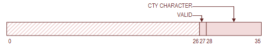
Figure 38 - CON: KS10 CTY Output Word (KS10 Memory Address 000033)
| Table 23 - CON: KS10 CTY Output Word (KS10 Memory Address 000032) | |||||||||||||||||||
|---|---|---|---|---|---|---|---|---|---|---|---|---|---|---|---|---|---|---|---|
| Bit(s) | Mnemonic | Description | |||||||||||||||||
| 0-26 | Reserved | Ignored for reads and writes. | |||||||||||||||||
| 27 | VALID |
Asserted by KS10 when character is available for the Console to read. Cleared by the Console after the character has been read. |
|||||||||||||||||
| 28-35 | CTY Character |
ASCII Character. Asserted by KS10 when character is available for the Console to read. Cleared by the Console after the character has been read. |
|||||||||||||||||
The procedure for transferring a character from the KS10 to the Console is a follows:
- The KS10 places a character with the VALID bit set in memory location 0000032.
- The KS10 interrupts the Console Processor.
- The Console Processor is interrupted.
- If the VALID bit is asserted, the Console Processor extracts the character from location 000032 bits 28-35 and outputs the character on the CTY serial output port. If the VALID bit is negated, the interrupt function should not process a character from the KS10. Note: the interrupt may indicate that another character should be transferred to the KS10.
- The Console Processor zeros location 000032. This zeros the VALID bit.
- The Console Processor Interrupts the KS10 by setting the KS10_INTR bit in the Console Control/Status Register.
The CTY Output Word should be initialized to zero by the Console Processor before starting the KS10.
| Table 24 - CON: KS10 KLINIK Input Word (KS10 Memory Address 000034) | |||||||||||||||||||
|---|---|---|---|---|---|---|---|---|---|---|---|---|---|---|---|---|---|---|---|
| Bit(s) | Mnemonic | Description | |||||||||||||||||
| 0-25 | Reserved | Ignored for reads and writes. | |||||||||||||||||
| 26-27 | KLCHR | Meaning: | |||||||||||||||||
| KLCHR[1:0] | Description | ||||||||||||||||||
| 0 | Nothing | ||||||||||||||||||
| 1 | Character Available | ||||||||||||||||||
| 2 | KLINIK Initialized | ||||||||||||||||||
| 3 | Carrier Lost | ||||||||||||||||||
| 28-35 | KLIICH | KLINIK character (ASCII). | |||||||||||||||||
| Table 25 - CON: KS10 KLINIK Output Word (KS10 Memory Address 000035) | |||||||||||||||||||
|---|---|---|---|---|---|---|---|---|---|---|---|---|---|---|---|---|---|---|---|
| Bit(s) | Mnemonic | Description | |||||||||||||||||
| 0-25 | Reserved | Ignored for reads and writes. | |||||||||||||||||
| 26 | KLHUP | KLINIK hang-up request | |||||||||||||||||
| 27 | VALID | KLINIK character available | |||||||||||||||||
| 28-35 | KLIICH | KLINIK character (ASCII). | |||||||||||||||||
| Table 26 - CON: KS10 Boot RH11 Address Word (KS10 Memory Address 000036) | |||||||||||||||||||
|---|---|---|---|---|---|---|---|---|---|---|---|---|---|---|---|---|---|---|---|
| Bit(s) | Mnemonic | Description | |||||||||||||||||
| 0-13 | Reserved | Ignored for reads and writes. | |||||||||||||||||
| 14-35 | ADDR | RH11 Base Address (including UBA). | |||||||||||||||||
| Table 27 - CON: KS10 Boot Unit Number (KS10 Memory Address 000037) | |||||||||||||||||||
|---|---|---|---|---|---|---|---|---|---|---|---|---|---|---|---|---|---|---|---|
| Bit(s) | Mnemonic | Description | |||||||||||||||||
| 0-32 | Reserved | Ignored for reads and writes. | |||||||||||||||||
| 33-35 | UNIT | Unit Select | |||||||||||||||||
| UNIT[2:0] | Description | ||||||||||||||||||
| 0 | Device 0. | ||||||||||||||||||
| 1 | Device 1. | ||||||||||||||||||
| 2 | Device 2. | ||||||||||||||||||
| 3 | Device 3. | ||||||||||||||||||
| 4 | Device 4. | ||||||||||||||||||
| 5 | Device 5. | ||||||||||||||||||
| 6 | Device 6. | ||||||||||||||||||
| 7 | Device 7. | ||||||||||||||||||
This 36-bit parameter gets copied (right justified) to a 16-bit Magtape Tape Control (MTTC) Register. It allows the operator to set the Tape Format, Tape Density, and Tape Transport (Slave Unit).
| Table 28 - CON: KS10 Boot Magtape Parameter Word (KS10 Memory Address 000040) | |||||||||||||||||||
|---|---|---|---|---|---|---|---|---|---|---|---|---|---|---|---|---|---|---|---|
| Bit(s) | Mnemonic | Description | |||||||||||||||||
| 0-24 | - |
Reserved Ignored. |
|||||||||||||||||
| 25-27 | DEN[2:0] | Density Select | |||||||||||||||||
| DEN[2:0] | Description | ||||||||||||||||||
| 0 | Format Unknown. | ||||||||||||||||||
| 1 | 800 BPI NRZ. | ||||||||||||||||||
| 2 | Format Unknown. | ||||||||||||||||||
| 3 | 800 BPI NRZ. | ||||||||||||||||||
| 4 | 1600 BPI PE. | ||||||||||||||||||
| 5 | Format Unknown. | ||||||||||||||||||
| 6 | Format Unknown. | ||||||||||||||||||
| 7 | Format Unknown. | ||||||||||||||||||
| 28-31 | FMT[3:0] | Format Select | |||||||||||||||||
| FMT[3:0] (decimal) |
Description | ||||||||||||||||||
| 0 |
PDP-10 Core Dump 4x 8-bit characters plus 1x 4-bit character. |
||||||||||||||||||
| 1 |
PDP-15 Core Dump 3x 6-bit characters. |
||||||||||||||||||
| 3 |
PDP-10 Normal 4x 8-bit characters. |
||||||||||||||||||
| 12 |
PDP-11 Normal 2x 8-bit characters. |
||||||||||||||||||
| 13 |
PDP-11 Core Dump 4x 4-bit characters. |
||||||||||||||||||
| 14 |
PDP-15 Normal 2x 8-bit characters. |
||||||||||||||||||
| 32 | - |
Reserved Ignored. |
|||||||||||||||||
| 33-35 | SS[2:0] |
Slave Select Specifies the unit number of the tape transport. |
|||||||||||||||||
The Console Interface is stable with no known deficiencies.
The diagnostic status of the KS10 Console Interface is summarized below:
                           DIAGNOSTIC                            Result
---------------------------------------------------------------- ------
DSLTA   DECSYSTEM 2020 TELETYPE TEST . . . . . . . . . . . . . . Pass
The KS10 FPGA consists of the KS10 CPU, Memory Subsystem, Console Subsystem, and some IO Bus Bridges.
IO Bus Bridge #1 supports a single RH-11 Massbus Controller attached to 8x RP06 Disk Drives. This interface was generally limited to this single peripheral because of Unibus performance issues.
IO Bus Bridge #2 was not originally implementable because of a KS10 backplane design limitation. This could be fixed in the KS10 FPGA, but no software would support it.
IO Bus Bridge #3 supports the bulk of the peripherals including a RH11 Massbus Controller attached to 8x TM03/TU77 Tape Drives, a DZ-11 8-Port Terminal Multiplexer, a LP20 Line Printer Controller, a DUP11 Communications Controller, and a KMC11 General Purpose Microcontroller.
IO Bus Bridge #4 supports 4x Unibus Exercisers which are used to test the IO Bridge (UBA) implementation.
Note: UBA1, UBA3, and UBA4 are testable by the DSUBA diagnostic.
The block diagram of the KS10 FPGA System is illustrated below:
Figure 39 - KS10: FPGA Block Diagram
Each of the major blocks has an independent wiki page which describes its design and operation.
The CPU module is a big module that glues all of the CPU subsections together. The subsections are illustrated below in the block diagram.

Figure 40 - CPU: Block Diagram
The CPU Code is located in the repository at: https://github.com/KS10FPGA/KS10FPGA/blob/master/fpga/ks10/cpu/cpu.v
The DEC KS10 ALU implementation used ten cascaded AM2901 4-bit processor slices. Some quick study showed that this did not work well with an FPGA implementation. Most FPGAs have optimized (very fast) carry logic that is provided to support counters and adders. This carry logic is much faster than the AM2902 parallel carry devices that supported the AM2901 slices in the KS10.
It turns out that the Verilog (and VHDL) synthesis tools could not infer that there was a single 40-bit carry chain from the Register Transfer Logic (RTL) description of the ten cascaded 4-bit slices. The resulting ALU was very slow.
A complicating architectural features of the PDP-10 ALU is the requirement to operate as a single 36-bit ALU or to operate as two independent 18-bit ALUs with no carry between the lower 18-bits and upper 18-bits. In order to accomplish this, the DEC engineers inserted an "AND Gate" in the middle of the carry chain to implement this feature. This limits the speed of the ALU. A block diagram of the DEC KS10 ALU is illustrated below.

Figure 41 - CPU: ALU Implementation (DEC KS10)
In the FPGA implementation, maintaining the integrity of the carry chain is very important to the speed of the ALU. To that end, the KS10 FPGA ALU is implemented both ways: as a single 40-bit wide ALU and as two independent 20-bit ALUs. Gates are cheap. The two different types of operations occur in parallel and the correct output is selected at the module output. Instead of the microcode enabling the carry between the two halves of the ALU, the microcode selects between the 40-bit ALU with the carry between the two halves and the 40-bit ALU with no carry between the two halves. This is illustrated below.

Figure 42 - CPU: ALU Implementation (KS10 FPGA)
This saves ‘cutting’ the 40-bit ALU carry chain in the middle and maintains the ALU speed.
This design change actually makes the description of the KS10 FPGA much simpler than the alternative. The operation of the 40-bit Q-shifter and the 40-bit F-shifter is much more visible than in the original DEC KS10 design.
So why is the ALU 40-bits wide instead of 36-bits?
Notice that the ALU is sign extended by two bits on the left, and zero padded by two bits on the right. The ALU is implemented with 4-bit wide slices. This implementation gave the DEC hardware access to the CRY2 (Carry 2) signal which is available at the interface between the first and second ALU chip. If this was implemented as a 36-bit wide ALU, this signal would be buried inside the am2901 chip and not accessible. There may be other signals also.
The FPGA implemented the CRY2 output completely differently.
The ALU Code is located in the repository at: https://github.com/KS10FPGA/KS10FPGA/blob/master/fpga/ks10/cpu/alu.v
The CPU Backplane Interface is the interface between the CPU and the backplane peripherals. The major function of the backplane is to determine the KS10 addressing mode. The KS10 understands four addressing modes. Namely:
- Extended Address – This is a full 20-bit address
- Physical Address – This is a 18-bit address
- Paged Address – This is a 20-bit virtual address
- WRU Address – A "Who Are You (WRU)" cycle is part of the interrupt acknowledge bus cycle. It addresses whatever device is asserting the highest priority interrupt request.

Figure 43 - CPU: Extended Addressing

Figure 44 - CPU: Physical Addressing

Figure 45 - CPU: Paged Addressing

Figure 46 - CPU: WRU Addressing
The Bus Address Multiplexer is simply a 36-bit wide 4-input multiplexer as illustrated below.
The Bus Interface Block diagram is illustrated below:

Figure 47 - CPU: Bus Interface Block Diagram
The Bus Interface Code is located in the repository at: https://github.com/KS10FPGA/KS10FPGA/blob/master/fpga/ks10/cpu/bus.v
The DBM Mux is used to access the SCAD, Timer, VMA Register, Bus Interface, and the Number field of the microcode. It can perform left-half/right-half bus swap and it is also used to do hardware byte selection when the byte is exactly 7 bits.
The DBM Mux is controlled by the microcode DBM Select (DBM_SEL) field, the byte select mux is controlled by the microcode SPECIAL (DBM_SPEC) field.
The DBM Block diagram is illustrated below:
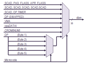
Figure 48 - CPU: DBM Block Diagram
The DBM Code is located in the repository at: https://github.com/KS10FPGA/KS10FPGA/blob/master/fpga/ks10/cpu/dbm.v
The DBUS module is essentially a 36-bit wide 4-to-1 multiplexer. The DBUS multiplexer selects between the FLAGS, the ALU Output (DP), the DBM Multiplexer, and the RAMFILE. On a memory read operation, the DBUS Multiplexer also selects between the RAMFILE (where the ACs are stored) if an AC is being read and memory if an AC is not being read.
When a memory request is made, the memory contents are supplied to this block via the DBM input. When a memory request is made to one of the AC registers, the forceRAMFILE bit is asserted and the contents of the RAMFILE is selected instead of the memory contents.
The forceRAMFILE signal is implemented very differently than the DEC KS10. In the KS10 FPGA implementation, the forceRAMFILE signal is asserted when the KS10 Bus input to the DBM Multiplexer is selected (i.e., during a memory read) and the VMA points to one of the ACs. That is VMA[18:31] is zero.
The Block Diagram of the DBUS Multiplexer is illustrated below:
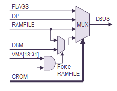
Figure 49 - CPU: DBUS Block Diagram
The DBUS Code is located in the repository at: https://github.com/KS10FPGA/KS10FPGA/blob/master/fpga/ks10/cpu/dbus.v
The microsequencer is a device that sequences through the microcode. The microsequencer has various inputs that control the execution sequence but the only output from the microsequencer block is the Control ROM (CROM) which provides the KS10 microcode. This microcode is used to control the various blocks of the KS10 hardware.
The DEC KS10 CPU was implemented using 2048 words of 108-bit wide horizontal microcode (as opposed to vertical microcode).
The microarchitecture supports 12-bit addressing of microcode (4096 words) but the DEC KS10 only implemented 2048 words microcode. The KS10 FPGA implements all 4096 words of microcode.
The microcode begins execution at address 0000. The microsequencer continuously re-executes instruction at address 0000 while the RESET signal is asserted and will only execute the next instruction after the RESET signal has been negated. This design assumes that the RESET negation is synchronized to the clock and that the RESET signal is asserted for a few clock cycles minimum to ensure that the instruction at address 0000 has been executed at least once. It also assumes that the instruction at address 0000 can be re-executed without any side-effects.
The Page Fail hardware is hard coded to vector to the Page Fail handler address. The Page Fail vector hardware is a bunch of “OR Gates” which just assert all of the microcode ROM address bits - therefore the Page Fail handler is located at 3777 (octal) for the DEC KS10 and 7777 (octal) for the KS10 FPGA. In general, the hardware addressing (Reset, Page Fail, Skip, and Dispatch) must match the addresses in the microcode. Therefore the hardware cannot be modified without appropriate changes to the microcode
The addressing the microsequencer is very minimalistic. Whereas a modern implementation might use a multiplexer to control the addressing, the KS10 uses simple “OR” gates. Therefore the SKIP, DISPATCH, and PAGE FAIL logic can only modify the addressing by setting bits – never clearing address bits.
On a normal microcode instruction, the SKIP, DISPATCH, and PAGE FAIL addresses are zero. The Control ROM supplies the next address from the microcode "Jump" field.
When a SKIP is to be performed (a primitive conditional branch-like instruction), the SKIP entity conditionally supplies an address of 0000 or 0001. This conditionally sets the LSB of the address. Of course the microcode must be designed such that the two destination addresses are appropriate.
The DISPATCH is similar to a SKIP except that an N-way branch can be executed. Again, the microcode must be designed such that all of the possible destination addresses are correct. The microcode uses a 512-way branch to quickly decode instruction opcodes, and additional N-way branches to quickly decode addressing modes. The opcode dispatch address is provided by the Dispatch ROM (DROM).
A block diagram of the Microsequencer is illustrated below.
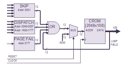
Figure 50 - CPU: Microsequencer Block Diagram
The major modules that implement the Microsequencer are detailed in the following sections.
The Microsequencer Code is located in the repository at: https://github.com/KS10FPGA/KS10FPGA/blob/master/fpga/ks10/cpu/useq/useq.v
The dispatch logic allows the microcode to perform an N-way branch based on a set of inputs. Implementation wise, it is a large multiplexer that is controlled by the microcode that provides a 12-bit dispatch address output.
The multiplexer is broken into two halves: the upper 8-bits are controlled independently from the lower 4-bits. This segregation into halves provides many 16-way dispatches and a few larger (up to 512-way) dispatches.
The instruction opcode decode dispatch is a 512-way dispatch where the address is supplied by the dispatch ROM.
The DEC KS10 dispatch logic was fairly convoluted (and very difficult to understand) in order to minimize logic and limit the size of the Dispatch ROM. For example, the instruction opcode decode dispatch is constrained to be in the address range between 1400 (octal) and 1700 (octal) in the microcode. The DEC KS10 design used a lot of hardwired logic to generate addresses in this address range - only the least significant bits were stored in the Dispatch ROM. In the KS10 FPGA, the entire dispatch address is stored in the dispatch ROM which significantly simplifies the logic description.
The logic synthesis tool is ‘smart enough’ to determine that the data contents of those ROM bits is constant for all addresses, remove the data from the ROM, and replace the ROM contents with hardwired logic just like the DEC KS10 – except that the design intent is much more evident in the FPGA version.
Obviously the design of dispatch logic and the design of the microcode must be compatible.
The Microsequencer Dispatch Code is located in the repository at: https://github.com/KS10FPGA/KS10FPGA/blob/master/fpga/ks10/cpu/useq/dispatch.v
The skip logic provides a means for the microcode to perform a conditional jump operation based on a boolean value. For the most part, the SKIP logic is a big 24:1 multiplexer that generates this boolean value.
The skipADDR output is always either 0000 (octal) for "no skip" condition or 0001 (octal) for a "skip" condition. Skips always occur from even addresses to odd addresses because the SKIP block addressing is implemented with an "OR Gate". It is not a multiplex operation
The Microseqencer Skip Code is located in the repository at: https://github.com/KS10FPGA/KS10FPGA/blob/master/fpga/ks10/cpu/useq/skip.v
This microsequencer stack provides a mechanism for the microcode to 'call' and 'return' from microcode subroutines.
The microsequencer stack is implemented quite a bit differently than the KS10 simply because the FPGA provides Dual Port RAMs.
- The addrOUT 'read' port of the Dual Port RAM provides the return address. This port always points to the top-of-stack and can always be read independently.
- The addrIN 'write' port of the Dual Port RAM is used to store the next 'call' address. This port always points to the address past the top-of-stack and can always be written independently.
A block diagram of the microseqencer stack is illustrated below.

Figure 51 - CPU: Microseqencer Stack
When the 'call' input to the block is asserted, the 'call' address is stored, the stack pointer is incremented and the return address automatically becomes available at the new top-of-stack.
When the 'ret' (return) input to the block is asserted, the stack pointer is decremented. The return address is always available at the addrOUT[0:11] port.
This implementation saves all the KS10 logic to dynamically change RAM address depending if a 'call' or 'return' instruction is being processed. It also allows the stack to always update in a single clock cycle.
The 'call' and 'return' operation of the microcode is quite a bit different than modern computers. The microsequencer stores the address of the 'call' instruction on the stack. The microcoded 'return' instruction must include a dispatch offset to the address in order to return to an instruction after the 'call' instruction.
When a Page Fail exception occurs, the microcode vectors to the 'Page Fail' handler - and simultaneously asserts the 'call' input. When the Page Fail handler code has completed execution, the microsequencer returns to the microcode instruction (the read or write operation that caused the Page Fail exception) and re-executes that instruction.
The Microseqencer Stack Code is located in the repository at: https://github.com/KS10FPGA/KS10FPGA/blob/master/fpga/ks10/cpu/useq/stack.v
The Control ROM contains the executable microcode of the microsequencer.
This module of the KS10 FPGA microsequencer is implemented significantly different than the DEC KS10 circuit but performs exactly the same function.
The DEC KS10 implementation has several implementation issues which must be addressed in an FPGA design. These are:
- The DEC KS10 microcode is stored in a RAM which must be loaded by the console processor at power-up. This is complicated and unnecessary. The FPGA can provide ROM for this function.
- The Control RAM is asynchronous. The FPGA provides synchronous memory.
In the KS10 FPGA, the Control RAM is replaced by a synchronous ROM which is not writeable. This simplifies the boot procedure. In the DEC KS10, the Control RAM microcode is post-processed to remove unused fields and rearrange the bits (I assume to optimize the hardware design). For example, the microcode listing defines a 108-bit wide microcode word whereas the hardware is only 96-bits wide. In the KS10 FPGA, the post-processing step has been elided as it is unnecessary. The Verilog synthesis tool is smart enough to identify and remove unused (or constant) data fields in the ROM. Also, the post-processing also adds parity which is not really necessary for the FPGA.
The DEC KS10 microsequencer had a 12-bit address which could have supported 4096 words of microcode; however, only half of the memory was actually implemented in the production hardware. Unfortunately, over time, the microcode grew to be larger 2048 words. When that occured, DEC shipped three version of the microcode – each matching a specific application. When you booted the machine, the boot disk (or tape) had the correct version of the microcode installed so boot process could load the correct microcode into Control RAM.
The various types of microcode are detailed below:
| Table 29 - CPU: KS10 Microcode Variations | |||||||||||||||||||
|---|---|---|---|---|---|---|---|---|---|---|---|---|---|---|---|---|---|---|---|
| Filename | Description | ||||||||||||||||||
| KS10.MCR |
Diagnostic microcode.
Includes TOPS10 paging and TOPS20 paging but does not include the UBABLT instructions. |
||||||||||||||||||
| T10KI.MCR |
TOPS10 microcode. Includes TOPS10 paging and UBABLT instructions but does not include TOPS20 paging. |
||||||||||||||||||
| T10KL.MCR |
TOPS20 microcode. Includes TOPS20 paging and UBABLT instructions but does not include TOPS10 paging. |
||||||||||||||||||
| CRAM4K.MCR |
*NEW* KS10 FPGA Unified microcode. Includes TOPS10 paging, TOPS20 paging, and UBABLT instructions. The APRID instruction reports 470130_010001 which is decoded below: |
||||||||||||||||||
| Option | Description | ||||||||||||||||||
| INHCST=1 | Allow inhibit of CST update if CSB = 0 | ||||||||||||||||||
| NOCST=0 | Include support for writing the CST> | ||||||||||||||||||
| NONSTD=0 | Standard microcode | ||||||||||||||||||
| UBABLT=1 | Support UBABLT instructions | ||||||||||||||||||
| KIPAG=1 | Support KI paging | ||||||||||||||||||
| KLPAG=1 | Support KL paging | ||||||||||||||||||
| MCV=130 | Microcode version | ||||||||||||||||||
| HO=0 | Hardware options | ||||||||||||||||||
| HSN=4097 | Hardware Serial Number | ||||||||||||||||||
Fortunately all three versions of microcode were derived from a single codebase using conditional compiles to remove microcode as required.
It was desirable for the KS10 FPGA to have the microcode in ROM. The additional microcode memory allowed the KS10 FPGA to support a functional superset of all of the DEC microcode.
Implementing the new version of microcode only required some minor modifications to the conditional compiles and some new build command files. A small design change was required to move the PAGE-FAIL entry point from 3777 (octal) to 7777 (octal) - which was a hardware constraint.
When a page failure occurs, the PAGE-FAIL address is generated in the hardware by setting all of the microcode address bits to one (using 12 OR gates). In the DEC KS10, the MSB of the address was unused and the microcode was limited to 2048 words, this created a PAGE-FAIL entry point of 3777 (octal) in the microcode. Once the full microcode memory was implemented, the correct entry point of 7777 (octal) was exposed to the microcode.
The contents of the Control ROM are extracted from the microcode listing file by a simple AWK script.
The Control ROM Code is located in the repository at: https://github.com/KS10FPGA/KS10FPGA/blob/master/fpga/ks10/cpu/useq/crom.v
The microcode output listing is located in the repository at: https://github.com/KS10FPGA/KS10FPGA/blob/master/fpga/ks10/cpu/useq/ks10.mcr
The microcode field definitions of the Control ROM is located in the repository at: https://github.com/KS10FPGA/KS10FPGA/blob/master/fpga/ks10/cpu/useq/crom.vh
The Dispatch ROM maps the instruction (from the Instruction Register) to the address of microcode in the Control ROM that decodes and executes that instruction.
The DEC KS10 implementation of the Dispatch ROM is problematic for an FPGA implementation because the DROM in the KS10 is asynchronous whereas FPGA memories are synchronous.
Fortunately the DROM is addressed by the Instruction Register (IR) - which is loaded synchronously. Therefore the KS10 FPGA absorbed a copy of the OPCODE portion of IR directly into Dispatch ROM addressing. Simply put: When we load the IR, we also simultaneously and synchronously lookup the contents of the Dispatch ROM.
The Dispatch ROM is a 512 x 36 bit synchronous ROM.
The DEC KS10 Dispatch ROM contents (as created by the microcode assembler) is post-processed to remove unused microcode fields and rearrange the bits. In the KS10 FPGA implementation, the Dispatch ROM contents matches the format of the microcode listing and the post-processing step is elided. The Verilog synthesis tool is smart enough to remove unused microcode fields from the ROM.
The Dispatch ROM contents are extracted from the microcode listing file by a simple AWK script.
The Dispatch ROM Code is located in the repository at: https://github.com/KS10FPGA/KS10FPGA/blob/master/fpga/ks10/cpu/useq/drom.v
The microcode output listing is located in the repository at: https://github.com/KS10FPGA/KS10FPGA/blob/master/fpga/ks10/cpu/useq/ks10.mcr
The microcode field definitions of the Dispatch ROM is located in the repository at: https://github.com/KS10FPGA/KS10FPGA/blob/master/fpga/ks10/cpu/useq/drom.vh
The KS10 CPU proper provides an 18-bit virtual address space for programs. The Pager provides an address translation mechanism that allows the KS10 CPU to access more than 256K words of memory.
The Pager adds two more bits of addressing which creates a 20-bit physical address from the 18-bit virtual address.
The Pager translates virtual addresses/page numbers to physical addresses/page numbers. There are 512 virtual pages which map to 2048 physical pages.
The address translation is illustrated below:
![]()
Figure 52 - CPU: Pager Address Translation
Physically, the pager sits between the CPU and the KS10 Backplane Bus on the address bus.
The DEC KS10 Page Translation Memory (Page Tables) were implemented using asynchronous memory which does not translate to an FPGA very efficiently. Since the Page Translation Memory is addressed by the VMA register and the VMA register is loaded synchronously, the FPGA implementation simply absorbs the VMA register into the Page Translation Memory addressing. In other words, when the VMA register is loaded, the VMA address is synchronously loaded into the Page Translation Memory. The Page Table is interleaved with odd and even memories so that the memory can be swept two entries at a time. The Page Table addressing is rearranged from that of the DEC KS10. On the DEC KS10 the two memories are interleaved by the MSB of the address. On the KS10 FPGA, the two memories are interleaved by the LSB of the address. When the interleaving is done this way, the Xilinx synthesis tool can infer a dual port memory with different aspect ratios on the two ports as follows:
- The Page Table is address by the write port as 256 x 30-bit memory. The 30-bit wide write port allows the page memory to be written and swept two entries at a time.
- The Page Table is address by the read port as 512 x 15-bit memory. The 15-bit wide read port allows for simple page lookups.
Referring to the block diagram below, the CPU writes data into the Page Table via the left port of dual port memory. The page translation data which consists of the virtual page number and the page flags is written to the dual port memory two entries at a time. This is consistent with the format of the User Page Tables and the Executive Page Tables. In general, the 'dp' (ALU) bus is the source of the data. The Page Table is also swept two entries at a time. This port is write-only.
On the right port of the dual port memory, the virtual address is used to address the Page Translation Memory. The output of this memory provides the Physical Page Number that is used to build the Physical Address. This port is read-only.

Figure 53 - CPU: Pager Block Diagram
The Page Flags are:
- Page Valid - this flag indicates that the page information has been initialized.
- Page Writable - this flag indicates that the page can be written.
- Page Cacheable – this flag indicates that the page is cacheable.
- Page User – this flag indicates that the page has only user-mode access privledges.
Note: All page flags are cleared when the Page Table is swept, although clearing the Page Valid flag is sufficient.
The Pager Code is located in the repository at: https://github.com/KS10FPGA/KS10FPGA/blob/master/fpga/ks10/cpu/pager.sv
The KS10 Priority Interrupt Controller is responsible for controlling the KS10 CPU’s response to interrupt requests. The Priority Interrupt Controller maintains a notion of the Current Interrupt Priority, whether an individual interrupt is enabled and whether the Priority Interrupt Controller is enabled.
When an interrupt input is asserted, the interrupt controller determines if the new interrupt is of a higher priority than the current interrupt state. If it is, and interrupt request to the KS10 CPU is made.
The KS10 supports three interrupt sources which are enumerated below:
- Arithmetic Processor (APR) Interrupts
- IO Bus (UBA) Interrupts
- Software Interrupts (Program Requests)
Each of the interrupt sources can provide 7 interrupt requests. The highest interrupt request priority is interrupt 1; the lowest interrupt request priority is interrupt 7.
The Priority Interrupt Register state is stored inside the ALU Register 14 (octal). When the "specLOADPI" microcode instruction is executed, the Priority Interrupt Register state is loaded from the ALU into the Priority Interrupt hardware via the DP bus. Notice that the format of the Priority Interrupt Register is closely resembles the operand of the Executive Mode RDPI instruction.
The format of the Priority Interrupt Register is enumerated in the following diagram:
Figure 54 - CPU: Priority Interrupt Register
The block diagram of the Priority Interrupt controller is illustrated below:

Figure 55 - CPU: Priority Interrupt Block Diagram
The Priority Interrupt code is located in the repository at: https://github.com/KS10FPGA/KS10FPGA/blob/master/fpga/ks10/cpu/pi.v
The RAMFILE contains storage for CPU implementation. This is essentially everything that is not stored in the ALU register set. The microcode does not use any of the KS10 memory.
The RAMFILE is a dedicated chunk of memory which is organized as 1Kx36. The RAMFILE is address as follows:
| Table 30 - CPU: KS10 RAMFILE Addressing | |||||||||||||||||||
|---|---|---|---|---|---|---|---|---|---|---|---|---|---|---|---|---|---|---|---|
| Address (octal) | Description | ||||||||||||||||||
| 0000-0017 | AC Block 0 |
||||||||||||||||||
| 0020-0037 | AC Block 1 |
||||||||||||||||||
| 0040-0057 | AC Block 2 |
||||||||||||||||||
| 0060-0077 | AC Block 3 |
||||||||||||||||||
| 0100-0117 | AC Block 4 |
||||||||||||||||||
| 0120-0137 | AC Block 5 |
||||||||||||||||||
| 0140-0157 | AC Block 6 |
||||||||||||||||||
| 0160-0177 | AC Block 7 |
||||||||||||||||||
| 0200-0777 | Workspace |
||||||||||||||||||
| 1000-1777 | Cache (Not implemented) |
||||||||||||||||||
Access to the RAMFILE ACs are selected using the AC field of the instruction as follows:
- Access to an AC in the current context using the AC field of the instruction.
- Access to an AC in the current context using the XR field of the instruction.
- Access to an AC in the previous context using the XR field of the instruction.
- Access to an AC in the current context using a plain address.
- Access to an AC in the previous context using a plain address.
- Access to RAMFILE storage.
- Access to the cache (Cache is not implemented)
In the original DEC KS10 implementation, this module was controlled only indirectly by the microcode. The relevant portions of the Control ROM microcode were multiplexed onto the DBM bus by the DBM multiplexer and the contents of the DBM bus were used to control the operation of the RAMFILE. Presumably this was done in order to limit the interconnect between circuit cards. The KS10 FPGA is implementation different in that it is controlled directly by the Control ROM microcode. The RAMFILE control paths through the DBM multiplexer have been elided. This is faster and simpler than the original design.
This RAMFILE addressing included a 74LS181 ALU in the DEC KS10 which was used for AC register-based indexing. Only the adder was required and that is all that is implemented. This adder is controlled by one of the overloaded usages of the CROM Number field.
The RAMFILE Code is located in the repository at: https://github.com/KS10FPGA/KS10FPGA/blob/master/fpga/ks10/cpu/ramfile.v
This module implements the instruction register. Various fields of the IR can be independently tested by the hardware.
The Step Count Adder (SCAD) is a small 10-bit accumulator and register set that is used for loop counting and for floating-point exponentiation.
This block includes the Step Count Register (SC) and the Floating-point Exponent Register (FE). The SCAD accumulator can be multiplexed to either register.
The Step Count Register (SC) is controlled by the microcode and used for generic loop counting. It is used, for example, in multi-bit shifts, multiplication, division, etc.
The Floating-point Exponent Register (FE) is used to keep track of the floating-point exponent during mathematical operations. In floating-point operation it is common for the exponent to be incremented or decremented as the ALU is shifted right or left.
The SCAD ALU can perform a load, add, subtract, bit-wise OR, increment, and decrement operations. A block diagram of the SCAD is illustrated below.

Figure 56 - CPU: SCAD Block Diagram
The SCAD Code is located in the repository at: https://github.com/KS10FPGA/KS10FPGA/blob/master/fpga/ks10/cpu/scad.v
The PDP-10 Interval Timer is used by the Monitor to measure elapsed time, run times, and time-of-day. The timer provides two basic units of time: a 10 microsecond clock where greater precision is required, and a 1 millisecond clock for normal operation.
The KS10 implements this function by providing a 12-bit timer that is clocked at 4.1 MHz. The RDTIME instruction microcode reads the timer register contents and divides the result by 41 to support the 10 microsecond timing. The 4.1 MHz clock is divided by 4096 in the 12-bit timer which overflows every 0.999024 milliseconds. This timer overflow generates a Timer Interrupt to the CPU. You might note that the timer interrupt actually occurs 0.1 percent fast. This timing error is fixed in the microcode so that the time-of-date is correct.
The Interval Timer Register is multiplexed into the CPU via the DBM Multiplexer. In the KS10 implementation (like the KS10), the Interval Timer Register input to the bottom half of the DBM is actually 18-bits wide: there are six bits of padding which are always zero, ten bits of timer, and the two timer LSBs which are always read as zero. This is illustrated below:

Figure 57 - CPU: Interval Timer Register
The microcode seems to read all 18-bits that are presented to the DBM and does not perform any masking. Whenever the Interval Timer Register is read, its two least significant bits are ignored so the register’s contents approximately represent a count in microseconds. The upper 6 bits are just unused and unnecessary.
The time base value is a 71-bit value that is stored in the RAMFILE. The 12 LSBs of the time base corresponds to the Interval Timer Register. The Write Time Base instruction (WRTIM) can initialize the time base as a number of milliseconds but cannot alter the Interval Timer contents - the 12 LSBs are ignored.
The KS10 FPGA actually does not contain a 4.1 MHz clock source like the DEC KS10. The KS10 FPGA generates the 4.1 MHz clock enable signal using a 32-bit Fractional-N divider operating at 50 MHz. The Fractional-N divider uses an accumulator instead of a divider to create the output signal - the accumulator maintains the fractional time when the count overflows. The accumulator keeps the average output frequency correct although the output will jitter by 20 nanoseconds as the output is still synchronous to the input clock. The 32-bit accumulator was chosen so that the frequency error caused by the Fractional-N Divider implementation is less than the frequency error of the oscillator device. Gates are cheap.
As stated above, a Timer Interrupt is generated when the Interval Timer overflows which is approximately every millisecond. Once asserted, the Timer Interrupt is cleared by a microcode instruction.
A block diagram of the TIMER module is illustrated below.

Figure 58 - CPU: Interval Timer Block Diagram
The TIMER Code is located in the repository at: https://github.com/KS10FPGA/KS10FPGA/blob/master/fpga/ks10/cpu/timer.v
The following table is the result of executing the "DSKFAA0 DECSYSTEM 2020 INSTRUCTION TIMING DIAGNOSTIC" on the KS10 FPGA and on a DEC KS10.
Thanks to Michael Thompson for providing benchmark timing for the DEC KS10.
| # | DEC KS10 Timing | (uS ) | KS10 FPGA Timing | (uS) | Speedup |
|---|---|---|---|---|---|
| 1 | BASIC CLOCK CYCLE IS 151 NSEC. | 0.151 | BASIC CLOCK CYCLE IS 32 NSEC. | 0.032 | 4.72 |
| 2 | INDEXING TAKES 303 NSEC. | 0.303 | INDEXING TAKES 80 NSEC. | 0.080 | 3.79 |
| 3 | INDIRECT TAKES 910 NSEC. | 0.910 | INDIRECT TAKES 240 NSEC. | 0.240 | 3.79 |
| 4 | INDEXING AND INDIRECT TAKES 910 NSEC. | 0.910 | INDEXING AND INDIRECT TAKES 240 NSEC. | 0.240 | 3.79 |
| 5 | MOVEI TAKES 1.22 USEC. | 1.220 | MOVEI TAKES 402 NSEC. | 0.402 | 3.03 |
| 6 | MOVSI TAKES 1.52 USEC. | 1.520 | MOVSI TAKES 482 NSEC. | 0.482 | 3.15 |
| 7 | MOVE FROM AC TAKES 1.52 USEC. | 1.520 | MOVE FROM AC TAKES 482 NSEC. | 0.482 | 3.15 |
| 8 | MOVE FROM MEMORY TAKES 1.52 USEC. | 1.520 | MOVE FROM MEMORY TAKES 482 NSEC. | 0.562 | 2.70 |
| 9 | MOVE TO MEMORY TAKES 2.28 USEC. | 2.280 | MOVE TO MEMORY TAKES 562 NSEC. | 0.562 | 4.06 |
| 10 | HRR FROM MEMORY TAKES 1.82 USEC. | 1.820 | HRR FROM MEMORY TAKES 562 NSEC. | 0.562 | 3.24 |
| 11 | HRRZ FROM MEMORY TAKES 1.82 USEC. | 1.820 | HRRZ FROM MEMORY TAKES 562 NSEC. | 0.562 | 3.24 |
| 12 | HLRZ FROM MEMORY TAKES 2.13 USEC. | 2.130 | HLRZ FROM MEMORY TAKES 642 NSEC. | 0.642 | 3.32 |
| 13 | SETZ TAKES 1.52 USEC. | 1.520 | SETZ TAKES 482 NSEC. | 0.482 | 3.15 |
| 14 | SETZM TAKES 1.97 USEC. | 1.970 | SETZM TAKES 482 NSEC. | 0.482 | 4.09 |
| 15 | SETZB TAKES 2.28 USEC. | 2.280 | SETZB TAKES 562 NSEC. | 0.562 | 4.06 |
| 16 | SETO TAKES 1.52 USEC. | 1.520 | SETO TAKES 482 NSEC. | 0.482 | 3.15 |
| 17 | SETOM TAKES 1.97 USEC. | 1.970 | SETOM TAKES 482 NSEC. | 0.482 | 4.09 |
| 18 | SETOB TAKES 2.28 USEC. | 2.280 | SETOB TAKES 562 NSEC. | 0.562 | 4.06 |
| 19 | JRST TAKES 914 NSEC. | 0.914 | JRST TAKES 241 NSEC. | 0.241 | 3.79 |
| 20 | JRSTF @MEM TAKES 4.25 USEC. | 4.250 | JRSTF @MEM TAKES 1.13 USEC. | 1.130 | 3.76 |
| 21 | JUMPA TAKES 1.22 USEC. | 1.220 | JUMPA TAKES 322 NSEC. | 0.322 | 3.79 |
| 22 | JUMP THAT DOESN'T TAKES 1.97 USEC. | 1.970 | JUMP THAT DOESN'T TAKES 482 NSEC. | 0.482 | 4.09 |
| 23 | JUMP THAT DOES TAKES 1.97 USEC. | 1.970 | JUMP THAT DOES TAKES 482 NSEC. | 0.482 | 4.09 |
| 24 | JSR TAKES 2.74 USEC. | 2.740 | JSR TAKES 644 NSEC. | 0.644 | 4.25 |
| 25 | JSP TAKES 1.82 USEC. | 1.820 | JSP TAKES 482 NSEC. | 0.482 | 3.78 |
| 26 | AOBJN TAKES 1.97 USEC. | 1.970 | AOBJN TAKES 482 NSEC. | 0.482 | 4.09 |
| 27 | SOJ TAKES 1.82 USEC. | 1.820 | SOJ TAKES 482 NSEC. | 0.482 | 3.78 |
| 28 | SOS TAKES 3.34 USEC. | 3.340 | SOS TAKES 803 NSEC. | 0.803 | 4.16 |
| 29 | AOJ TAKES 1.82 USEC. | 1.820 | AOJ TAKES 482 NSEC. | 0.482 | 3.78 |
| 30 | AOS TAKES 3.34 USEC. | 3.340 | AOS TAKES 803 NSEC. | 0.803 | 4.16 |
| 31 | JFFO (1B0) TAKES 3.95 USEC. | 3.950 | JFFO (1B0) TAKES 1.04 USEC. | 1.040 | 3.80 |
| 32 | JFFO (1B35) TAKES 14.55 USEC. | 14.550 | JFFO (1B35) TAKES 3.85 USEC. | 3.850 | 3.78 |
| 33 | PUSH TAKES 2.73 USEC. | 2.730 | PUSH TAKES 643 NSEC. | 0.643 | 4.25 |
| 34 | POP TAKES 3.79 USEC. | 3.790 | POP TAKES 883 NSEC. | 0.883 | 4.29 |
| 35 | MUUO TAKES 15.34 USEC. | 15.340 | MUUO TAKES 3.05 USEC. | 3.050 | 5.03 |
| 36 | LUUO TAKES 4.07 USEC. | 4.070 | LUUO TAKES 722 NSEC. | 0.722 | 5.64 |
| 37 | PUSHJ TAKES 2.73 USEC. | 2.730 | PUSHJ TAKES 723 NSEC. | 0.723 | 3.78 |
| 38 | ADD IMMEDIATE TAKES 1.67 USEC. | 1.670 | ADD IMMEDIATE TAKES 482 NSEC. | 0.482 | 3.46 |
| 39 | ADD FROM MEMORY TAKES 1.97 USEC. | 1.970 | ADD FROM MEMORY TAKES 562 NSEC. | 0.562 | 3.51 |
| 40 | ADD TO MEMORY TAKES 4.15 USEC. | 4.150 | ADD TO MEMORY TAKES 903 NSEC. | 0.903 | 4.60 |
| 41 | MUL (9 ADD/SUB|18 SHIFTS) TAKES 15.76 USEC. | 15.760 | MUL (9 ADD/SUB|18 SHIFTS) TAKES 4.10 USEC. | 4.100 | 3.84 |
| 42 | IMULI TAKES 14.70 USEC. | 14.700 | IMULI TAKES 3.93 USEC. | 3.930 | 3.74 |
| 43 | DIV TAKES 22.81 USEC. | 22.810 | DIV TAKES 4.02 USEC. | 4.020 | 5.67 |
| 44 | IDIVI TAKES 19.40 USEC. | 19.400 | IDIVI TAKES 4.10 USEC. | 4.100 | 4.73 |
| 45 | FIX A FLOATING POINT ONE TAKES 13.04 USEC. | 13.040 | FIX A FLOATING POINT ONE TAKES 3.37 USEC. | 3.370 | 3.87 |
| 46 | FLTR AN INTERGER ONE TAKES 17.74 USEC. | 17.740 | FLTR AN INTERGER ONE TAKES 3.45 USEC. | 3.450 | 5.14 |
| 47 | FAD (1 RIGHT SHIFT) TAKES 6.83 USEC. | 6.830 | FAD (1 RIGHT SHIFT) TAKES 1.68 USEC. | 1.680 | 4.07 |
| 48 | FAD (8 SHIFT RIGHT|3 LEFT) TAKES 11.07 USEC. | 11.070 | FAD (8 SHIFT RIGHT|3 LEFT) TAKES 2.65 USEC. | 2.650 | 4.18 |
| 49 | FMP (7 ADD/SUB|14 SHIFTS) TAKES 18.34 USEC. | 18.340 | FMP (7 ADD/SUB|14 SHIFTS) TAKES 4.02 USEC. | 4.020 | 4.56 |
| 50 | FDV TAKES 22.74 USEC. | 22.740 | FDV TAKES 4.02 USEC. | 4.020 | 5.66 |
| 51 | DMOVE FROM MEMORY TAKES 2.73 USEC. | 2.730 | DMOVE FROM MEMORY TAKES 722 NSEC. | 0.722 | 3.78 |
| 52 | DMOVEM TO MEMORY TAKES 3.50 USEC. | 3.500 | DMOVEM TO MEMORY TAKES 803 NSEC. | 0.803 | 4.36 |
| 53 | DFAD (1 RIGHT SHIFT) TAKES 12.73 USEC. | 12.730 | DFAD (1 RIGHT SHIFT) TAKES 3.21 USEC. | 3.210 | 3.97 |
| 54 | DFAD (8 SHIFT RIGHT|1 LEFT) TAKES 14.86 USEC. | 14.860 | DFAD (8 SHIFT RIGHT|1 LEFT) TAKES 3.76 USEC. | 3.760 | 3.95 |
| 55 | DFMP (7 ADD/SUB|32 SHIFTS) TAKES 63.35 USEC. | 65.350 | DFMP (7 ADD/SUB|32 SHIFTS) TAKES 3.78 USEC. | 3.780 | 17.29 |
| 56 | DFDV TAKES 52.74 USEC. | 52.740 | DFDV TAKES 3.78 USEC. | 3.780 | 13.95 |
| 57 | CONO PI TAKES 7.28 USEC. | 7.280 | CONO PI TAKES 1.61 USEC. | 1.610 | 4.52 |
| 58 | CONI PI TAKES 2.88 USEC. | 2.880 | CONI PI TAKES 723 NSEC. | 0.723 | 3.98 |
| 59 | CONO PAG TAKES 109.13 USEC. | 109.130 | CONO PAG TAKES 27.45 USEC. | 27.450 | 3.98 |
| 60 | DATAO PAG LOAD UBR TAKES 109.94 USEC. | 109.940 | DATAO PAG LOAD UBR TAKES 27.45 USEC. | 27.450 | 4.01 |
| 61 | DATAO PAG LOAD AC BLK TAKES 3.65 USEC. | 3.650 | DATAO PAG LOAD AC BLK TAKES 963 NSEC. | 0.963 | 3.79 |
| 62 | WRIO TAKES 14.25 USEC. | 14.250 | WRIO TAKES 2.45 USEC. | 2.450 | 5.82 |
| 63 | RDIO TAKES 15.46 USEC. | 15.460 | RDIO TAKES 2.78 USEC. | 2.780 | 5.56 |
| 64 | LOGICAL SHIFT (35 PLACES LEFT) TAKES 7.43 USEC. | 7.430 | LOGICAL SHIFT (35 PLACES LEFT) TAKES 2.19 USEC. | 2.190 | 3.39 |
| 65 | LOGICAL SHIFT (35 PLACES RIGHT) TAKES 7.43 USEC. | 7.430 | LOGICAL SHIFT (35 PLACES RIGHT) TAKES 2.19 USEC. | 2.190 | 3.39 |
| 66 | LOGICAL SHIFT COMBINED (71 PLACES LEFT) TAKES 25.46 USEC. | 25.460 | LOGICAL SHIFT COMBINED (71 PLACES LEFT) TAKES 2.25 USEC. | 2.250 | 11.32 |
| 67 | LOGICAL SHIFT COMBINED (71 PLACES RIGHT) TAKES 25.76 USEC. | 25.760 | LOGICAL SHIFT COMBINED (71 PLACES RIGHT) TAKES 2.25 USEC. | 2.250 | 11.45 |
| 68 | INCREMENT BYTE POINTER TAKES 3.04 USEC. | 3.040 | INCREMENT BYTE POINTER TAKES 724 NSEC. | 0.724 | 4.20 |
| 69 | ILDB (7 BITS) TAKES 5.92 USEC. | 5.920 | ILDB (7 BITS) TAKES 1.45 USEC. | 1.450 | 4.08 |
| 70 | IDPB (7 BITS) TAKES 6.98 USEC. | 6.980 | IDPB (7 BITS) TAKES 1.61 USEC. | 1.610 | 4.34 |
| 71 | ILDB (6 BITS) TAKES 9.86 USEC. | 9.860 | ILDB (6 BITS) TAKES 2.77 USEC. | 2.770 | 3.56 |
| 72 | IDPB (6 BITS) TAKES 15.01 USEC. | 15.010 | IDPB (6 BITS) TAKES 4.71 USEC. | 4.710 | 3.19 |
| 73 | LDB (7 BITS|POS 6) TAKES 4.70 USEC. | 4.700 | LDB (7 BITS|POS 6) TAKES 1.20 USEC. | 1.200 | 3.92 |
| 74 | LDB (7 BITS|POS 13) TAKES 4.70 USEC. | 4.700 | LDB (7 BITS|POS 13) TAKES 1.20 USEC. | 1.200 | 3.92 |
| 75 | LDB (7 BITS|POS 20) TAKES 4.70 USEC. | 4.700 | LDB (7 BITS|POS 20) TAKES 1.20 USEC. | 1.200 | 3.92 |
| 76 | LDB (7 BITS|POS 27) TAKES 4.70 USEC. | 4.700 | LDB (7 BITS|POS 27) TAKES 1.20 USEC. | 1.200 | 3.92 |
| 77 | LDB (7 BITS|POS 34) TAKES 4.70 USEC. | 4.700 | LDB (7 BITS|POS 34) TAKES 1.20 USEC. | 1.200 | 3.92 |
| 78 | DPB (7 BITS|POS 6) TAKES 5.76 USEC. | 5.760 | DPB (7 BITS|POS 6) TAKES 1.37 USEC. | 1.370 | 4.20 |
| 79 | DPB (7 BITS|POS 13) TAKES 5.76 USEC. | 5.760 | DPB (7 BITS|POS 13) TAKES 1.37 USEC. | 1.370 | 4.20 |
| 80 | DPB (7 BITS|POS 20) TAKES 5.76 USEC. | 5.760 | DPB (7 BITS|POS 20) TAKES 1.37 USEC. | 1.370 | 4.20 |
| 81 | DPB (7 BITS|POS 27) TAKES 5.76 USEC. | 5.760 | DPB (7 BITS|POS 27) TAKES 1.37 USEC. | 1.370 | 4.20 |
| 82 | DPB (7 BITS|POS 34) TAKES 5.76 USEC. | 5.760 | DPB (7 BITS|POS 34) TAKES 1.37 USEC. | 1.370 | 4.20 |
| 83 | LDB (6 BITS|POS 5) TAKES 9.70 USEC. | 9.700 | LDB (6 BITS|POS 5) TAKES 2.23 USEC. | 2.230 | 4.35 |
| 84 | LDB (6 BITS|POS 11) TAKES 8.79 USEC. | 8.790 | LDB (6 BITS|POS 11) TAKES 2.02 USEC. | 2.020 | 4.35 |
| 85 | LDB (6 BITS|POS 17) TAKES 7.88 USEC. | 7.880 | LDB (6 BITS|POS 17) TAKES 2.01 USEC. | 2.010 | 3.92 |
| 86 | LDB (6 BITS|POS 23) TAKES 9.40 USEC. | 9.400 | LDB (6 BITS|POS 23) TAKES 2.11 USEC. | 2.110 | 4.45 |
| 87 | LDB (6 BITS|POS 29) TAKES 8.49 USEC. | 8.490 | LDB (6 BITS|POS 29) TAKES 2.13 USEC. | 2.130 | 3.99 |
| 88 | LDB (6 BITS|POS 35) TAKES 7.58 USEC. | 7.580 | LDB (6 BITS|POS 35) TAKES 1.96 USEC. | 1.960 | 3.87 |
| 89 | DPB (6 BITS|POS 5) TAKES 14.86 USEC. | 14.860 | DPB (6 BITS|POS 5) TAKES 5.02 USEC. | 5.020 | 2.96 |
| 90 | DPB (6 BITS|POS 11) TAKES 13.95 USEC. | 13.950 | DPB (6 BITS|POS 11) TAKES 4.66 USEC. | 4.660 | 2.99 |
| 91 | DPB (6 BITS|POS 17) TAKES 13.04 USEC. | 13.040 | DPB (6 BITS|POS 17) TAKES 4.10 USEC. | 4.100 | 3.18 |
| 92 | DPB (6 BITS|POS 23) TAKES 12.13 USEC. | 12.130 | DPB (6 BITS|POS 23) TAKES 3.42 USEC. | 3.420 | 3.55 |
| 93 | DPB (6 BITS|POS 29) TAKES 11.22 USEC. | 11.220 | DPB (6 BITS|POS 29) TAKES 3.13 USEC. | 3.130 | 3.58 |
| 94 | DPB (6 BITS|POS 35) TAKES 10.31 USEC. | 10.310 | DPB (6 BITS|POS 35) TAKES 2.75 USEC. | 2.750 | 3.75 |
| 95 | JFCL TAKES 1.67 USEC. | 1.670 | JFCL TAKES 402 NSEC. | 0.402 | 4.15 |
| 96 | CAI NO-OP TAKES 1.22 USEC. | 1.220 | CAI NO-OP TAKES 322 NSEC. | 0.322 | 3.79 |
| 97 | CAI THAT DOESN'T SKIP TAKES 2.13 USEC. | 2.130 | CAI THAT DOESN'T SKIP TAKES 482 NSEC. | 0.482 | 4.42 |
| 98 | CAI THAT SKIPS TAKES 2.13 USEC. | 2.130 | CAI THAT SKIPS TAKES 483 NSEC. | 0.483 | 4.41 |
| 99 | CAM NO-OP TO AC TAKES 1.97 USEC. | 1.970 | CAM NO-OP TO AC TAKES 482 NSEC. | 0.482 | 4.09 |
| 100 | CAM TO AC THAT DOESN'T SKIP TAKES 2.43 USEC. | 2.430 | CAM TO AC THAT DOESN'T SKIP TAKES 562 NSEC. | 0.562 | 4.32 |
| 101 | CAM TO AC THAT SKIPS TAKES 2.43 USEC. | 2.430 | CAM TO AC THAT SKIPS TAKES 563 NSEC. | 0.563 | 4.32 |
| 102 | CAM NO-OP TO MEMORY TAKES 1.97 USEC. | 1.970 | CAM NO-OP TO MEMORY TAKES 482 NSEC. | 0.482 | 4.09 |
| 103 | CAM TO MEMORY THAT DOESN'T SKIP TAKES 2.43 USEC. | 2.430 | CAM TO MEMORY THAT DOESN'T SKIP TAKES 562 NSEC. | 0.562 | 4.32 |
| 104 | CAM TO MEMORY THAT SKIPS TAKES 2.43 USEC. | 2.430 | CAM TO MEMORY THAT SKIPS TAKES 563 NSEC. | 0.563 | 4.32 |
| 105 | TLN NO SKIP TAKES 2.28 USEC. | 2.280 | TLN NO SKIP TAKES 562 NSEC. | 0.562 | 4.06 |
| 106 | TLN SKIP TAKES 2.28 USEC. | 2.280 | TLN SKIP TAKES 563 NSEC. | 0.563 | 4.05 |
| 107 | TRN NO SKIP TAKES 1.97 USEC. | 1.970 | TRN NO SKIP TAKES 482 NSEC. | 0.482 | 4.09 |
| 108 | TRN SKIP TAKES 1.98 USEC. | 1.980 | TRN SKIP TAKES 483 NSEC. | 0.483 | 4.10 |
| 109 | TDN NO SKIP TAKES 2.28 USEC. | 2.280 | TDN NO SKIP TAKES 562 NSEC. | 0.562 | 4.06 |
| 110 | TDN SKIP TAKES 2.28 USEC. | 2.280 | TDN SKIP TAKES 563 NSEC. | 0.563 | 4.05 |
| 111 | TSN NO SKIP TAKES 2.58 USEC. | 2.580 | TSN NO SKIP TAKES 642 NSEC. | 0.642 | 4.02 |
| 112 | TSN SKIP TAKES 2.59 USEC. | 2.590 | TSN SKIP TAKES 644 NSEC. | 0.644 | 4.02 |
| 113 | SKIP TO AC THAT DOESN'T TAKES 2.58 USEC. | 2.580 | SKIP TO AC THAT DOESN'T TAKES 642 NSEC. | 0.642 | 4.02 |
| 114 | SKIP TO AC THAT DOES TAKES 2.59 USEC. | 2.590 | SKIP TO AC THAT DOES TAKES 644 NSEC. | 0.644 | 4.02 |
| 115 | SKIP TO MEMORY THAT DOESN'T TAKES 2.58 USEC. | 2.580 | SKIP TO MEMORY THAT DOESN'T TAKES 642 NSEC. | 0.642 | 4.02 |
| 116 | SKIP TO MEMORY THAT DOES TAKES 2.59 USEC. | 2.590 | SKIP TO MEMORY THAT DOES TAKES 644 NSEC. | 0.644 | 4.02 |
| 117 | EQV AC TO AC TAKES 1.82 USEC. | 1.820 | EQV AC TO AC TAKES 562 NSEC. | 0.562 | 3.24 |
| 118 | EQV MEMORY TO AC TAKES 1.82 USEC. | 1.820 | EQV MEMORY TO AC TAKES 562 NSEC. | 0.562 | 3.24 |
| 119 | EXCHANGE AN AC WITH AN AC TAKES 2.58 USEC. | 2.580 | EXCHANGE AN AC WITH AN AC TAKES 642 NSEC. | 0.642 | 4.02 |
| 120 | EXCHANGE AN AC WITH MEMORY TAKES 2.58 USEC. | 2.580 | EXCHANGE AN AC WITH MEMORY TAKES 642 NSEC. | 0.642 | 4.02 |
| 121 | EXECUTE TAKES 2.12 USEC. | 2.120 | EXECUTE TAKES 561 NSEC. | 0.561 | 3.78 |
| 122 | BLT MEMORY TO MEMORY TAKES 7.43 USEC. | 7.430 | BLT MEMORY TO MEMORY TAKES 1.77 USEC. | 1.770 | 4.20 |
| 123 | BLT AC TO MEMORY TAKES 7.43 USEC. | 7.430 | BLT AC TO MEMORY TAKES 1.77 USEC. | 1.770 | 4.20 |
The CPU design is very stable with the exception of the Pager. At this point, it is simpler to document what does not work correctly.
-
DSKCGB fails the EXTEND/EDIT instruction on the Start Significance (SIGST) pattern only. All other tests pass.
See https://github.com/KS10FPGA/KS10FPGA/issues/4 for additional information.
-
DSKDA fails the BLK instruction test. The BLT instruction should be interruptable and is not due to a Pager issue. All other tests pass.
See https://github.com/KS10FPGA/KS10FPGA/issues/5 for additional information.
-
DSKEB fails. The KS10 FPGA uses high-speed single-cycle memory and operates at cache speeds. DSKEB measures loop timing and expects to see a faster execution speed with the cache enable - which doesn't occur. DSKEB fails as expected. This is as intended and will not be fixed.
See https://github.com/KS10FPGA/KS10FPGA/issues/6 for additional information.
-
DSKEA - DECSYSTEM 2020 PAGING HARDWARE DIAGNOSTIC has numerous failures. The pager has serious issues.
-
DSKEC - DECSYSTEM KS10 KL-PAGING TEST has numerous failures. The pager has serious issues.
The diagnostic status of the KS10 CPU is summarized below:
                           DIAGNOSTIC                            Result
---------------------------------------------------------------- ------
DSKAAA0 DECSYSTEM 2020 BASIC INSTRUCTION DIAGNOSTIC ( 1) . . . . Pass
DSKABA0 DECSYSTEM 2020 BASIC INSTRUCTION DIAGNOSTIC ( 2) . . . . Pass
DSKACA0 DECSYSTEM 2020 BASIC INSTRUCTION DIAGNOSTIC ( 3) . . . . Pass
DSKADA0 DECSYSTEM 2020 BASIC INSTRUCTION DIAGNOSTIC ( 4) . . . . Pass
DSKAEA0 DECSYSTEM 2020 BASIC INSTRUCTION DIAGNOSTIC ( 5) . . . . Pass
DSKAFA0 DECSYSTEM 2020 BASIC INSTRUCTION DIAGNOSTIC ( 6) . . . . Pass
DSKAGA0 DECSYSTEM 2020 BASIC INSTRUCTION DIAGNOSTIC ( 7) . . . . Pass
DSKAHA0 DECSYSTEM 2020 BASIC INSTRUCTION DIAGNOSTIC ( 8) . . . . Pass
DSKAIA0 DECSYSTEM 2020 BASIC INSTRUCTION DIAGNOSTIC ( 9) . . . . Pass
DSKAJA0 DECSYSTEM 2020 BASIC INSTRUCTION DIAGNOSTIC (10) . . . . Pass
DSKAKA0 DECSYSTEM 2020 BASIC INSTRUCTION DIAGNOSTIC (11) . . . . Pass
DSKALA0 DECSYSTEM 2020 BASIC INSTRUCTION DIAGNOSTIC (12) . . . . Pass
DSKAMA0 DECSYSTEM 2020 BASIC INSTRUCTION DIAGNOSTIC (13) . . . . Pass
DSKBAA0 DECSYSTEM 2020 BASIC INSTRUCTION RELIABILITY DIAGNOSTIC  Pass
DSKCAA0 DECSYSTEM 2020 ADVANCED INSTRUCTION DIAGNOSTIC (1) . . . Pass
DSKCBA0 DECSYSTEM 2020 ADVANCED INSTRUCTION DIAGNOSTIC (2) . . . Pass
DSKCCA0 DECSYSTEM 2020 ADVANCED INSTRUCTION DIAGNOSTIC (3) . . . Pass
DSKCDA0 DECSYSTEM 2020 ADVANCED INSTRUCTION DIAGNOSTIC (4) . . . Pass
DSKCEA0 DECSYSTEM 2020 ADVANCED INSTRUCTION DIAGNOSTIC (5) . . . Pass
DSKCFC0 DECSYSTEM 2020 ADVANCED INSTRUCTION DIAGNOSTIC (6) . . . Pass
DSKCGB0 DECSYSTEM 2020 ADVANCED INSTRUCTION DIAGNOSTIC (7) . . .   Fail
DSKDAB0 DECSYSTEM 2020 CPU AND MEMORY RELIABILITY DIAGNOSTIC . .   Fail
DSKEAA0 DECSYSTEM 2020 PAGING HARDWARE DIAGNOSTIC  . . . . . . .   Fail
DSKEBA0 KS10 - CACHE DIAGNOSTIC  . . . . . . . . . . . . . . . . Pass
DSKECB0 KS10 - KL-PAGING DIAGNOSTIC  . . . . . . . . . . . . . .   Fail
DSKFAA0 DECSYSTEM 2020 INSTRUCTION TIMING DIAGNOSTIC . . . . . . Pass
Click on the underlined Pass/Fail issues links in the table above for more information regarding status.
The KS10 had a memory controller card plus a maximum of 8 memory cards slots where each DEC memory card provided maximum of 64 MW of memory – for a total of 512 KW of memory. The memory cards used 16kx1 dynamic RAM chips.
The DEC part number for the Memory Controller was M8618 and is designated as MMC on the schematics. The DEC part number for the MOS Memory Array was M8629 and is designated as MMA on the schematics.
It is common folklore that the KS10 was architecturally limited to 512 KW of memory. This is not true. This was either a memory technology limitation or a marketing limitation but was not an architectural limitation. The KS10 internal memory address paths have always supported 20-bit addressing.
There were modifications made by ADP that provided 1 MW of memory instead of 512 KW of memory. This modification involved modifying the DEC Memory Controller and DEC Unibus Adapter by adding "white-wires". I'm guessing that these two boards did not provide all of the addressing that was required for a full memory configuration and that the modification to the UBA was to add an extra address line to the IO Pager circuit.
Oddly enough, the CPU and Backplane properly properly implemented all of address wires. Even stranger, as pointed out by Michael Thompson, there must have been plans for the M8629 memory board to support different memory configurations. Per the schematic, the M8629-AA supported 16K chips, the M8629-BA supported 64K chips, and the M8629-CA supported 256K chips. The M8629 even provides some jumper wires on the board to select the proper board capacity (see M8629 Sheet MMA1). Apparently only the M8629-AA with 16K chips (64 KW) was never manufactured by DEC. If the M8629-CA had been manufactured, a single board would have provided 1MW of memory.
Once the modifications were performed, the ADP system was populated with 4x of the original 64KW memory boards plus 3x new 256 KW memory boards.
Note: Thanks to Michael Thompson for providing information detailed information about the ADP memory modifications. For additional information about a KS10 with the ADP system modifications, see: https://www.ricomputermuseum.org/collections-gallery/equipment/dec-pdp-10-ks10-4165.
The KS10 FPGA Memory Controller attempts to be fully compatible with the DEC KS10 Memory Controller. Whereas the DEC KS10 Memory Controller interfaces to multiple boards utilizing dynamic MOS memory, the KS10 FPGA Memory Controller interfaces to a single Pipelined SSRAM device.
The Memory Controller occupies the UBA0 address area and the system only supports one memory controller.
The Memory Controller Registers are defined below:
| Table 31 - MEM: Memory Controller Register Summary | |||||||||||||||||||
|---|---|---|---|---|---|---|---|---|---|---|---|---|---|---|---|---|---|---|---|
| UBA | Register Offset | Register Name | Access | Register Description | |||||||||||||||
| 0 | 100000 | MSR | 36-bit word (R/W) |
Memory Status Register | |||||||||||||||
The Memory Status Register is a 36-bit IO register located at IO Address o100000.
The Memory Status Register in the DEC KS10 provides status information about KS10 memory status.
The KS10 FPGA does not require or support memory Error Detection and Correction (EDAC). The Memory Status Register bits are implemented as required to be compatible with a real KS10 but none of the underlying functionality is implemented. Having said that, most of the functionality of the Memory Controller is not tested.
The Memory Status Register is a 'strange' register. Many of the bits are different depending on whether the register is being read or written. See below.

Figure 59 - MEM: Memory Status Register (Read)

Figure 60 - MEM: Memory Status Register (Write)
| Table 32 - MEM: Memory Status Register (MSR) Definitions | |||||||||||||||||||
|---|---|---|---|---|---|---|---|---|---|---|---|---|---|---|---|---|---|---|---|
| Bit(s) | Mnemonic | R/W | Read Description | Write Description | |||||||||||||||
| 0 | EH | R/W |
Error Hold EH is asserted when any Memory Error occurs. Not implemented in the KS10 FPGA. Always read as zero by the KS10 FPGA. |
Error Hold EH is negated by writing a '1' to EH. Not implemented in the KS10 FPGA. Writes are ignored by the KS10 FPGA. |
|||||||||||||||
| 1 | UE | R/W |
Uncorrectable Read Error UE is asserted when an Uncorrectable Read Error occurs. Not implemented in the KS10 FPGA. Always read as zero by the KS10 FPGA. |
Uncorrectable Read Error UE is negated by writing a '1' to UE. Not implemented in the KS10 FPGA. Writes are ignored by the KS10 FPGA. |
|||||||||||||||
| 2 | RE | R/W |
Refresh Error RE is asserted when a memory Refresh Error occurs. Not implemented in the KS10 FPGA. Always read as zero by the KS10 FPGA. |
Refresh Error RE is negated by writing a '1' to RE. Not implemented in the KS10 FPGA. Writes are ignored by the KS10 FPGA. |
|||||||||||||||
| 3 | PE | R/W |
Parity Error PE is asserted when:
PE is negated when '0' is written to PE. The KS10 FPGA does not implement bus parity detection. |
Parity Error PE is asserted when '1' is written to PE. PE is negated when '0' is written to PE. |
|||||||||||||||
| 4 | EE | R |
ECC Enable EE is asserted if the last write to the ECC Disable (MSR[ED]) bit was '0'. EE is negated if the last write to the ECC Disable (MSR[ED]) bit was '1'. |
ECC Enable Writes are ignored. |
|||||||||||||||
| 5:11 | ECC | R |
ECC Check Bits ECC[5:11] contain the 7 ECC check bits from the last Uncorrectable Read Error. These check bits are named CP, C40, C20, C10, C4, C2, and C1. Not implemented in the KS10 FPGA. Always read as zero by the KS10 FPGA. |
Reserved Writes are Ignored. |
|||||||||||||||
| 12 | PF | R/W |
Power Fail PF is asserted at power-up. PF is negated by writing '0' to PF. |
Power Fail PF is asserted at power-up. PF is negated by writing '0' to PF. |
|||||||||||||||
| 13 | - | R |
Reserved Always read as zero. |
Reserved Writes are ignored. |
|||||||||||||||
| 14:27 | ERA[14:27] | R |
Error Address bits 14:27 Provides address bits 14-27 of the last memory error. Not implemented in the KS10 FPGA. Always read as zero by the KS10 FPGA. |
Reserved Writes are ignored. |
|||||||||||||||
| 28:34 | ERA[28:34] FCB[28:34] |
R W |
Error Address bits 28-34 Provides address bits 28-34 of the last memory error. Not implemented in the KS10 FPGA. Always read as zero by the KS10 FPGA. |
Force Check Bits There are 7 ECC check bits named CP, C40, C20, C10, C4, C2, and C1; and there are 7 FCB bits that are similarly named CP, C40, C20, C10, C4, C2, and C1. When you assert for example, FCB bit C40, the ECC check bit C40 is inverted and is re-written to the last memory location that was addressed. This permits robust memory testing as well as memory ECC testing. Not implemented in the KS10 FPGA. Writes are ignored by the KS10 FPGA. Note: I could be very wrong about how this works. |
|||||||||||||||
| 35 | ERA[35] ED |
R W |
Error Address bit 35 Provides address bit 35 of the last memory error. Not implemented in the KS10 FPGA. Always read as zero by the KS10 FPGA. |
ECC Disable Writing a '0' to ED asserts the ECC Enable bit (MSR[EE] = '1'). Writing a '1' to ED negates the ECC Enable bit (MSR[EE] = '0'). |
|||||||||||||||
The KS10 FPGA prototypes have supported two different memory interfaces. The Xilinx Spartan 6 prototype implemented a 1M x 36-bit NoBL Pipelined Synchronous Static RAM (SSRAM) while the DE10-nano prototype implemented a 2M × 18 NoBL Flow-Through Synchronous Static RAM (SSRAM).
These implementations will be described in the following sections.
Both devices are very high speed memories.
The DE10-nano prototype elected to use a slightly more complex memory architecture in order to save FPGA pins. This interface includes a Cypress CY7C1463KV33 18-bit SSRAM that operates with a 2-word burst
The SSRAM interface operates at four times the CPU clock rate in order to perform these burst memory reads and memory writes in a single CPU clock cycle. In this system, the 36-bit data word is stored in two adjacent memory locations. Specifically, the burst operation is designed such that the high word of memory (DATA[0:17]) is stored first in memory followed by the low word of memory (DATA[18:35]).
The burst mode addressing is relatively simple: the memory address is shifted left by 1 bit and is concatinated with A0 as the LSB. The high word occupies the even SSRAM addresses (A0 negated) while the low word occupies the odd addresses (A0 asserted). This is illustrated in the figure below.

Figure 61 - MEM: Burst Mode SSRAM Address and Data Mapping
Although the SSRAM burst control pin (ADV/LD#) is wired to the FPGA, it is not used and is always negated. The output enable signal (ssramOE_N) is asserted during both read and write cycles. This is permitted per the datasheet. The SSRAM controls the data bus direction by pipelining the SSRAM Write Enable (SSRAM_WE_N) signal.
The diagram below illustrates the SSRAM bus cycles that have been implemented.
Figure 62 - MEM: SSRAM Write Cycle followed by and Read Cycle
In read cycles, the SSRAM Write Enable (SSRAM_WE_N) is always negated.
In T1:
- At the beginning of T1, the FPGA asserts the address of the high-word of memory (DATA[0:17]) on the SSRAM Address Bus. SSRAM_A[0] is negated.
- At the middle of T1, the SSRAM device samples the address of the high-word from the SSRAM Address Bus.
In T2:
- At the beginning of T2, the FPGA asserts the address of the low-word of memory (DATA[18:35]) on the SSRAM Address Bus. SSRAM_A[0] is asserted.
- At the middle of T2, the SSRAM device samples the address of the low-word from the SSRAM Address Bus.
- At the middle of T2, the SSRAM drives the high-word of data (D[0:17]) onto the SSRAM Data bus.
In T3:
- At the beginning of T3, the FPGA captures the high-word of data (D[0:17]). SSRAM_A[0] is negated - but this is a "don't care" for read cycles.
- At the middle of T3, the SSRAM drives the low-word of data (D[18:35]) onto the SSRAM Data bus.
In T4:
- At the beginning of T4, the FPGA captures the high-word of data (D[18:35]). SSRAM_A[0] is asserted.
In T1:
- The FPGA speculatively starts a read cycle because it hasn't determined the cycle type before the beginning of T1. The data from this read cycle is eventually ignored. During T1, The FPGA determines that this is a write cycle and prepares for write operation in T2 and later.
- At the beginning of T1, the FPGA asserts the address of the high-word of memory (DATA[0:17]) on the SSRAM Address Bus. SSRAM_A[0] is negated.
- At the middle of T1, the SSRAM device samples the address of the high-word from the SSRAM Address Bus. Again, this is just speculation.
In T2:
- At the beginning of T2, the FPGA asserts the address of the low-word of memory (DATA[18:35]) on the SSRAM Address Bus. SSRAM_A[0] is asserted. Also, the FPGA asserts SSRAM Write Enable (SSRAM_WE_N) which facilitates writing to the low-word of memory.
- At the middle of T2, the SSRAM device samples the address of the low-word from the SSRAM Address Bus. Also the SSRAM drives the high-word of data (D[0:17]) onto the SSRAM Data bus. The data read from the FPGA was speculated incorrectly and is ignored by the FPGA.
In T3:
- At the beginning of T3, the FPGA asserts the address of the high-word of memory (DATA[0:17]) on the SSRAM Address Bus. SSRAM_A[0] is negated. Again, the FPGA asserts SSRAM Write Enable (SSRAM_WE_N) which facilitates writing to the high-word of memory. Lastly, the FPGA drives the low-word of memory (DATA[18:35]) on the SSRAM Data Bus.
- At the middle of T3, the SSRAM samples SSRAM_D[18:35].
In T4:
- At the beginning of T4, the FPGA asserts the address of the low-word of memory (DATA[18:35]) on the SSRAM Address Bus. SSRAM_A[0] is asserted. The FPGA negates SSRAM Write Enable which starts a dummy read cycle where the data will be available and ignored in the next T1. Lastly, the FPGA drives the high-word of memory (DATA[0:17]) on the SSRAM Data Bus.
- At the middle of T4, the SSRAM samples SSRAM_D[0:17].
From the description, you can observe that A0 is negated in T1, is asserted in T2, is negated in T3, and is asserted in T4. In other words, A0 just alternates.
It is also worth noting that the SSRAM is read high-word first because the read cycle starts in T1, while the SSRAM is written low-word first because the write cycle starts in T2.
This interface supports the older prototype board. It is not actively maintained.
The Xilinx Spartan 6 KS10 Memory Interface is design to accommodate a Cypress CY7C1460AV33 1M x 36-bit NoBL Pipelined Synchronous Static RAM (SSRAM).
This memory has a 2 stage pipeline between the address signals and the memory array. The device is capable of operating at a 166 MHz clock rate.
Because the memory device has a 2 stage pipeline, portions of the memory controller operate at four times the CPU clock rate. This creates the illusion that memory reads and memory writes complete in a single CPU clock cycle. For write operations the write enable signal (ssramWE_N) is asserted at the beginning (rising edge) of T2. The SSRAM device registers the address (ssramADDR[0:19]) and data (ssramDATA[0:35]) on the rising edge of the SSRAM Clock (ssramCLK). The write operation actually completes two clock cycles later at the beginning (rising edge) of T4. The address and data buses are generally unstable or contain the previous address and data during T1.
The memWRITE signal controls the SSRAM data bus interface direction. If the memWRITE signal is asserted, the FPGA asserts the busDATAI[0:35] signals onto the SSRAM data bus. If the memWRITE signal is negated, the FPGA tristates SSRAM data bus and the SSRAM data may be read from the SSRAM device.
In this mode, the SSRAM device will configure the direction of the SSRAM data bus based on the operation of the write enable signal (ssramWE_N). The data bus will be an output from the SSRAM except for two clock cycles after the write enable signal is asserted.
For reads, the address is sampled continuously but the memory device is enabled only in T4.

Figure 63 - MEM: SSRAM Read Cycle

Figure 64 - MEM: SSRAM Read Cycle Timing Parameters

Figure 65 - MEM: SSRAM Write Cycle

Figure 66 - MEM: SSRAM Write Cycle Timing Parameters
The Memory Controller and Memory is stable with no known deficiencies.
The diagnostic status of the KS10 memory controller (and memory) is summarized below:
                           DIAGNOSTIC                             RESULT
----------------------------------------------------------------  ------
DSMMAB0 DECSYSTEM 2020 KS10 1024K MEM DIAG . . . . . . . . . . .  Pass
DSMMBA0 DECSYSTEM 2020 BLT/FLOATING 1-0 MEMORY EXERCISER TEST  .  Pass
DSMMCB0 DECSYSTEM 2020 FAST AC DIAGNOSTIC  . . . . . . . . . . .  Pass
DSMMDC0 DECSYSTEM 2020 MEM DIAG  . . . . . . . . . . . . . . . .  Pass
The KS10 FPGA IO Bus Bridge interfaces the peripherals on the IO bus to the KS10 backplane bus. In the DEC KS10, the IO Bus was Unibus. Here the KS10 FPGA diverts significantly from the DEC design and implements a completely different, but compatible IO Bus design. This includes register-compatibility and compatible Virtual Address to Physical Address translation for the IO Bus. For these reasons, I've chosen to call this a IO Bus Bridge instead of a Unibus Adapter - although many places use the term Unibus and UBA to maintain consistency with the DEC KS10 documentation. This is discussed below.
The DEC KS10 system architecture supported up to three IO Bridges that interfaced the KS10 backplane to standard Unibus Devices. These UnibusAdapters are commonly referred to as UBA1, UBA3, and UBA4; although the KS10 Technical Manual only documents the possibility of UBA1 and UBA3.
Apparently there is a limitation in the KS10 backplane wiring that prevents the use of UBA2, but UBA4 works in "non-standard" systems. TOPS-10 looks for devices on all four but never finds UBA2 installed. TOPS-20 only looks for UBA1, UBA3, and UBA4.
Lastly, and most importantly, the DSUBA diagnostic will test UBA1, UBA3, and UBA4 per below. The KS10 FPGA does implement the mostly undocumented Maintenance Loopback Modes as required to pass the DSUBA diagnostics.
DECSYSTEM 2020 UNIBUS ADAPTER EXERCISER  [ DSUBA ]
VERSION 0.4, SV=0.3, CPU#=2020, MCV=130, MCO=470, HO=0, KASW=003740 000000

TTY SWITCH CONTROL ? - 0,S OR Y  - 0
SWITCHES = 000000 000000

MEMORY MAP =
FROM     TO          SIZE/K
00000000 03777777       1024


WHICH UNIBUS ADAPTER? (1,3,4):
The IO Bus Bridge is fully parameterized so all of these configurations are supported by the UBA Verilog module. UBA1, UBA3, and UBA4 are implemented in the FPGA. Each UBA adapter can currently support up to 5 devices.
In KS10 systems, UBA1 supports the RH11 Massbus Disk Controller exclusively. This is done to meet the disk performance requirements. UBA3 supports the RH11 Massbus Tape Controller and everything else in the KS10 system. For now, UBA4 has four Unibus Exercisers (UBE) devices attached which are used to test the UBA.
The KS10 FPGA IO Bus implementation provides a synchronous 36-bit non-multiplexed control/address bus and a 36-bit data bus whereas Unibus provides an asynchronous 16-bit address bus and an 18-bit data bus. The KS10 FPGA IO Bus also uses significantly fewer clock cycles to implement the IO bus protocol.
| Table 33 - UBA: Register Summary | |||||||||||||||||||
|---|---|---|---|---|---|---|---|---|---|---|---|---|---|---|---|---|---|---|---|
| Register Offset | Register Name | Access | Register Description | ||||||||||||||||
| 763000 - 763077 |
UBAPAG | 36-bit word (R/W) |
IO Bridge Paging RAM | ||||||||||||||||
| 763100 | UBASR | 36-bit word (R/W) |
IO Bridge Status Register | ||||||||||||||||
| 763101 | UBAMR | 36-bit word (W) |
IO Bridge Maintenance Register | ||||||||||||||||
The IO Bridge Status Register (UBASR) is a 36-bit IO register located at IO Address o763100 and is compatible with the Unibus Status Register of the DEC KS10.

Figure 67 - UBA: Status Register (UBASR)
| Table 34 - UBA: Status Register (UBASR) Definitions - IO Address 763100 | |||||||||||||||||||
|---|---|---|---|---|---|---|---|---|---|---|---|---|---|---|---|---|---|---|---|
| Bit(s) | Mnemonic | R/W | Description | ||||||||||||||||
| 18 | TMO | R/W |
Adapter Timeout The TMO bit is set under the following conditions:
The TMO bit is negated by:
|
||||||||||||||||
| 19 | BMD | R |
Bad Memory Data Not implemented. Always read as zero. Writes are ignored. |
||||||||||||||||
| 20 | BPE | R |
Bus Parity Error Not implemented. Always read as zero. Writes are ignored. |
||||||||||||||||
| 21 | NXD | R/W |
Non Existent Device The NXD bit is asserted when accessing an IO device attached to this IO Bridge that does not exist; i.e., no IO device acknowledges a request at the IO address that was provided. The NXD bit is negated by:
|
||||||||||||||||
| 22 | - | - |
Reserved Always read as zero. Writes are ignored. |
||||||||||||||||
| 23 | - | - |
Reserved Always read as zero. Writes are ignored. |
||||||||||||||||
| 24 | HI | R |
HI Interrupt HI is asserted when there is an active IRQ on BR7 or BR6. Writes are ignored. |
||||||||||||||||
| 25 | LO | R |
LO Interrupt LO is asserted when there is an active IRQ on BR5 or BR4. Writes are ignored. |
||||||||||||||||
| 26 | PWR | R |
Power Fail The PWR bit is asserted when any of the IO devices asserts the ACLO signal; otherwise PWR is negated. None of the proper IO devices generate the ACLO signal, however the PWR bit is tested by the Unibus Exerciser (UBE) in DSUBA TEST45. The KS10 FPGA version of the IO Bus does not implement the Unibus DCLO signal since it is not used by anything and is not tested.
Writes are ignored. |
||||||||||||||||
| 28 | DXF | R/W |
Disable Transfer Not implemented. DXF is asserted by writing a '1' to DXF. DXF is negated by:
|
||||||||||||||||
| 29 | INI | R/W |
Initialize. AKA IO Bridge Clear Writing '1' to INI resets all devices on this IO Bridge. The KS10 has a one-shot that asserts this signal for 1 μS. This bit remains asserted only for that period. |
||||||||||||||||
| 30:32 | PIH | R/W |
Priority Interrupt High PIH maps the priority of the high priority device interrupts, devINTR[7] and devINTR[6], to the CPU interrupt priority defined by the PIH register. PIH is set by writing to this register. PIH is cleared by:
Note: There are seven CPU interrupt priorities - Priority 1 through Priority 7. Setting PIH to 0 disables all high priority interrupts from this IO Bridge. |
||||||||||||||||
| 33:35 | PIL | R/W |
Priority Interrupt Low PIL maps the priority of the low priority device interrupts, devINTR[5] and devINTR[4], to the CPU interrupt priority defined by the PIL register. PIL is set by writing to this register. PIL is cleared by:
Note: There are seven CPU interrupt priorities - Priority 1 through Priority 7. Setting PIL to 0 disables all low priority interrupts from this IO Bridge. |
||||||||||||||||
The IO Bridge Maintenance Register (UBAMR) is a 36-bit IO register located at IO Address o763101 and controls the maintenance loopback feature of the IO Bus Bridge. The UBAMR is compatible with the Unibus Maintenance Register of the DEC KS10. Only some of the Maintenance Loopback features of the IO Bridge is implemented as required to pass the DSUBA diagnostics.

Figure 68 - UBA: Maintenance Register (UBAMR)
| Table 35 - UBA: Maintenance Register (UBAMR) Definitions - IO Address 763101 | |||||||||||||||||||
|---|---|---|---|---|---|---|---|---|---|---|---|---|---|---|---|---|---|---|---|
| Bit(s) | Mnemonic | R/W | Description | ||||||||||||||||
| 0:34 | - | - |
Reserved. Always read as zero. Writes are ignored. |
||||||||||||||||
| 35 | MAINT | W |
Maintenance Mode MAINT is asserted by writing a '1' to MAINT. MAINT is negated by:
Always read as zero. |
||||||||||||||||
The KS10 supports a 20-bit physical address while the IO devices only support a limited 16-bit address. The IO Bus Bridge provides a Paging mechanism that allows IO devices to access the entire physical memory of the KS10. This address translation is illustrated below.

Figure 69 - UBA: Address Translation (Paging)
Please be aware that KS10 address and data is big-endian (Bit 0, on the left, is the Most Significant Bit (MSB)) while the IO Bus address and data (like Unibus) is little-endian (Bit 0, on the right, is the Least Significant Bit (LSB)).
The Address Translation is managed by a Translation (Paging) Memory that is located on the IO Bus Bridge.
The IO Bus Page Translation Memory is a sequence of memory locations at IO Address o76300 – o763077 and is register-compatible with the Unibus Paging Memory of the DEC KS10.
The paging memory is a lookup table that is used to translate the IO Virtual Address to the KS10 Physical Address. For each of the 64 Virtual Pages there are a possible 2048 Physical Pages.
The format of the IO Bridge Paging Memory when written is summarized below.

Figure 70 - UBA: Paging RAM (Write)
The format of the IO Bridge Paging Memory when read is summarized below.

Figure 71 - UBA: Paging RAM (Read)
The bit definitions of the Paging RAM are defined below. The "Read Reverse", "Enable 16-bit IO Transfers", and "Fast Transfer Mode" bits in the paging RAM control the type of KS10 Bus to IO Bus (Unibus) translation that occurs in the IO Bridge.
| Table 36 - UBA: Paging RAM Definitions - IO Addresses 763000-763077 | |||||||||||||||||||
|---|---|---|---|---|---|---|---|---|---|---|---|---|---|---|---|---|---|---|---|
| Bit(s) | Mnemonic | R/W | Description | ||||||||||||||||
| 5/18 | RRV | R/W |
Read Reverse In normal mode (not "Read Reverse" mode), when a 16-bit or 18-bit NPR operation occurs, the access to the Even Word occurs first and writes the entire 36-bit word. The access to the Odd Word is a Read-Pause-Write (or Read/Modify/Write) access. In Read Reverse mode, when a 16-bit or 18-bit Word is being accessed, the access to the Odd Word occurs first and is a Read-Pause-Write (or Read/Modify/Write) access. The access to the Even Word is also a Read-Pause-Write (or Read/Modify/Write) access. |
||||||||||||||||
| 6/19 | E16 | R/W |
Enable 16-bit Enable 16-bit NPR operations and disable 18-bit NPR operations. |
||||||||||||||||
| 7/20 | FTM | R/W |
Fast Transfer Mode. In this mode, reads from even words on Unibus are stored in the UBA and not immediately transferred to memory. When the odd word is accessed, the even word and odd word is transferred in a single 36-bit KS10 operation. This is used by the RH11 to efficiently transfer data been memory and disk drives. This is implemented as required for the maintenance loopback diagnostics. This bit is ignored for IO Bus transactions which are always 36-bit. |
||||||||||||||||
| 8/21 | VLD | R/W |
Page valid. This bit is set when the page data is loaded. |
||||||||||||||||
| 16:26 25:36 |
PPM | R/W | Physical Page Number. | ||||||||||||||||
An IO Bridge Page Failure occurs when:
- IO Address Bit 17 is asserted. This bit must be zero for a memory operation.
- The paging data for this page is requests Fast Transfer Mode (FTM) and IO Address Bit 0 is asserted.
- The paging data for this page is requests Fast Transfer Mode (FTM) and IO Address Bit 1 is asserted.
- The paging data for this page is not valid (see VLD bit).
Paging only occurs on memory operations and never occurs on IO operations.
In Fast Transfer Mode (FTM), the device transfers 36-bit data and the two LSBs must be zero. The more modern term for this would be an "alignment error".
The KS10 supports 36-bit IO addressing to internal devices, 16/18-bit IO addressing to UBA devices, and 8-bit addressing to UBA devices.
The DEC UBA data translation between the KS10 Backplane Bus and IO Bus is governed by a few rules:
- In normal mode (not "Read Reverse" mode), when a 16-bit or 18-bit NPR operation occurs, the access to the Even Word normally occurs first and is a normal access. The access to the Odd Word is a Read-Pause-Write (or Read/Modify/Write) access.
- In Read Reverse mode, when a 16-bit or 18-bit NPR operation occurs, the access to the Odd Word occurs first and is a Read-Pause-Write (Read/Modify/Write) access. The access to the Even Word is also a Read-Pause-Write (Read/Modify/Write) access.
- In normal mode (not "Read Reverse" mode), when a Byte is being accessed, the access to the Even Word Low Byte occurs first and is a normal access. The accesses to the Even Word High Byte, Odd Word Low Byte, Odd Word High Byte follow in order and are Read-Pause-Write(Read/Modify/Write) accesses.
- In Fast Transfer Mode, accesses to Even Words are stored by the IO Bridge. When the Odd Word is accessed, the 36-bit result of these two operations are combined into a single 36-bit access.
Note: I don't really know if Read Reverse mode works with Byte Transfers or works in Fast Transfer Mode.
Byte and Word translation is based on the two LSBs of the IO address and is illustrated below.

Figure 72 - UBA: Byte and Word Translation into a 36-bit Word
| Table 37 - UBA: Byte and Word Address Translation | |||||||||||||||||||
|---|---|---|---|---|---|---|---|---|---|---|---|---|---|---|---|---|---|---|---|
| BYTE OP |
UBA A1 |
UBA A0 |
UBA Transaction Description | ||||||||||||||||
| 0 | 0 | 0 | Even word | ||||||||||||||||
| 0 | 1 | 0 | Odd word | ||||||||||||||||
| 1 | 0 | 0 | Even word, low byte | ||||||||||||||||
| 1 | 0 | 1 | Even word, high byte | ||||||||||||||||
| 1 | 1 | 0 | Odd word, low byte | ||||||||||||||||
| 1 | 1 | 1 | Odd word, high byte | ||||||||||||||||
Having acknowledged the DEC UBA design, the KS10 FPGA is not implemented the same way. As noted previously, the KS10 FPGA IO Bus is 36-bit wide and does not require the IO Bus Bridge to perform any of these data translation operations. The interface and IO translation between the IO device and the KS10 backplane is performed by the device. For example, the RH11 always operates in Fast Transfer Mode.
| Table 38 - UBA: Supported Device NPR Operations | |||||||||||||||||||
|---|---|---|---|---|---|---|---|---|---|---|---|---|---|---|---|---|---|---|---|
| Device | NPR Mode |
NPR In |
NPR Out |
Comments | |||||||||||||||
| DUP11 | N/A | No | No | Does not support NPR operations. | |||||||||||||||
| DZ11 | N/A | No | No | Does not support NPR operations. | |||||||||||||||
| KMC11 | RPW | Yes | Yes | Supports both memory and IO NPR operations. | |||||||||||||||
| LP20 | RPW | Yes | No |
Supports NPR operations to load translation RAM and to transfer printer data from memory to the character buffer. |
|||||||||||||||
| RH11 | FTM | Yes | Yes | Always Fast Transfer Mode (FTM) | |||||||||||||||
| UBE | FTM RPW RRV |
Yes | Yes | Testing only. | |||||||||||||||
SMMON CMD - DSUBA

DECSYSTEM 2020 UNIBUS ADAPTER EXERCISER  [ DSUBA ]
VERSION 0.4, SV=0.3, CPU#=2020, MCV=130, MCO=470, HO=0, KASW=003740 000000

TTY SWITCH CONTROL ? - 0,S OR Y  - 0
SWITCHES = 000000 000000

MEMORY MAP =
FROM     TO          SIZE/K
00000000 03777777       1024


WHICH UNIBUS ADAPTER? (1,3,4):1


***** NO EXERCISERS ON UNIBUS *****

 - TESTING UNIBUS ADAPTER 1


***** WARNING: NO EXERCISERS ON BUS,-UBE MEDIATED TESTS ABORTED *****
END PASS 1.
Although there seems to be address definitions and interrupt definitions 12 Unibus Exercisers (UBEs), the DSUBA diagnostic probes for them in order and only uses the first four that are found - even if more are provided.
SMMON CMD - DSUBA

DECSYSTEM 2020 UNIBUS ADAPTER EXERCISER  [ DSUBA ]
VERSION 0.4, SV=0.3, CPU#=2020, MCV=130, MCO=470, HO=0, KASW=003740 000000

TTY SWITCH CONTROL ? - 0,S OR Y  - 0
SWITCHES = 000000 000000

MEMORY MAP =
FROM     TO          SIZE/K
00000000 03777777       1024


WHICH UNIBUS ADAPTER? (1,3,4):4

UBE     BASE ADDRESS    VECTOR
______________________________
01      4770000         0510
02      4770020         0520
03      4770040         0530
04      4770060         0540

END PASS 1.
The diagnostic status of the KS10 IO Bus Bridge is summarized below:
                           DIAGNOSTIC                            Result
---------------------------------------------------------------- ------
DSUBAC0 DECSYSTEM 2020 UNIBUS ADAPTER EXERCISER  . . . . . . . . Pass
In-essence, the RH11 is a Unibus to Massbus bus bridge.
The KS10 FPGA includes one or two RH11 Massbus Controllers - depending on how the KS10 FPGA is configured. In the KS10 system, one RH11 is attached to the UBA1 Unibus Bridge and provides a Massbus interface to up 8 Disk Drives. An optional second RH11 is attached to UBA3 and provides a Massbus interface to control up to 8 Tape Controllers (or Tape Formatters).
There were several variants of the RH11; most of them were intended for use in PDP-11 systems. Of these variants, the RH11-C was created for use in the KS10 and uses the M9724-YA card which adds a Unibus "Bus Hog" mode (enabled by a jumper) that greatly improves the performance of Disk Drives. In "Bus Hog" mode, the RH11-C can do unarbitrated Unibus block transfers. Normally, the RH11-C that interfaces with the Disk Drives is configured for "Bus Hog" mode while the RH11-C that is controlling the Tape Drives is not configured for "Bus Hog" mode. Note: when the RH11-C is configured in "Bus Hog" mode, the RH11-C can be the only peripheral device attached to that Unibus since the DMA (or as DEC call it: "NPR") operations are unarbitrated.
The KS10 FPGA always arbitrates IO Bus accesses; therefore this "Bus Hog" mode is not implemented.
Lastly, the KS10 FPGA "Massbus" implementation looks nothing like the DEC "Massbus". The KS10 FPGA implementation is a 36-bit wide synchronous bus that is similar to the KS10 Backplane Bus and the KS10 FPGA IO Bus implementation.
The following RH11 documentation is available:
- RH11-B Engineering Drawings (Schematic), Rev A, 1977
- RH11-C Engineering Drawings (Schematic), Rev A, 1977
- RH11-A, RH11-B Engineering Drawings (Schematic), Rev J, 1978
- RH11-A, RH11-B Engineering Drawings (Schematic), Rev K, 1978
- RH11-A, RH11-B Option Description, Rev B, 1979
- RH11 Peripheral Controller Course Documents, 1979
- RH11/RH70 Massbus Controllers - A Self-Paced Course, 1979
The RH11 FPGA implementation is fully parameterized and may be configured as follows:
| Table 39 - RH: Configuration | |||||||||||||||||||
|---|---|---|---|---|---|---|---|---|---|---|---|---|---|---|---|---|---|---|---|
| Device | UBA | Interrupt | Interrupt Vector | Base Address | Use | ||||||||||||||
| RH11 #1 | UBA1 | 6 | 000254 | 776700 | Disk Controller | ||||||||||||||
| RH11 #3 | UBA3 | 6 | 000224 | 772440 | Tape Controller | ||||||||||||||
The Massbus Interface between the RH11 and the disk and tape devices is implemented as a SystemVerilog 'interface' which encapsulates the Massbus signals. This interface does support both disk drives and tape drives.
The RH11 Massbus Controller exposes two different types of registers to the programmer:
- Controller Registers that are located in the RH11 Massbus Controller that apply to all disk/tape drives, and
- Device Registers that are located inside the individual disk/tape drives and apply only to that device.
In a real KS10, the Controller Registers were part of the RH11 Controller and the Device Registers were located in the disk drives or tape drives on the device side of the Massbus cabling. This hierarchy is maintained in the KS10 FPGA although the Massbus cabling is more a logical concept than a physical implementation.
The RH11 Massbus Controller maintains state and reports status that is applicable to the entire Massbus system. For example the Controller RPCS2 register has 3 bits which select which of the 8 disk/tape devices is addressed to receive commands or report status. That controller state includes the following registers:
| Table 40 - RH: Device Registers | |||||||||||||||||||
|---|---|---|---|---|---|---|---|---|---|---|---|---|---|---|---|---|---|---|---|
| Unibus Address |
Register Name |
R/W | Register Description | ||||||||||||||||
|
776700 772440 |
RHCS1 RPCS1 MTCS1 |
R/W |
Control and Status Register #1 Portions of this register are in the RH11. Portions of this register are in the Massbus device and vary by device. |
||||||||||||||||
| 776702 772442 |
RHWC | R/W | Word Count Register |
||||||||||||||||
| 776704 772444 |
RHBA | R/W | Bus Address Register | ||||||||||||||||
| 776710 772450 |
RHCS2 | R/W | Control and Status Register #2 | ||||||||||||||||
| 776722 772462 |
RHDB | R/W | Data Buffer Register | ||||||||||||||||
The Massbus register are mapped at various locations in the RH11 address space. In implementation, a ROM maps IO Bus addresses (Unibus) to Massbus addresses.
The exact details of Massbus registers depend on the types of devices that are attached to the Massbus - the RH11 just passes the Massbus registers through the RH11 interface. Note: RPxx disk drives are different that RMxx disk drives; and tape drives are different than disk drives.
The Massbus Register addresses are summarized below:
| Table 41 - RH: Massbus Register Address Cross Reference | |||||||||||||||||||
|---|---|---|---|---|---|---|---|---|---|---|---|---|---|---|---|---|---|---|---|
| Reg # (octal) | RP Register Name | RM Register Name | TU Register Name | Comment | |||||||||||||||
| 0 | RPCS1 | RMCS1 | MTCS1 | Compatible between RP, RM, and TU. | |||||||||||||||
| 1 | RPDS | RMDS | MTDS | Compatible between RP, RM, and TU. | |||||||||||||||
| 2 | RPER1 | RMER1 | MTER | Compatible between RP, RM, and TU. | |||||||||||||||
| 3 | RPMR | RMMR1 | MTMR | Compatible between RP, RM, and TU. | |||||||||||||||
| 4 | RPAS | RMAS | - | ||||||||||||||||
| 5 | RPDA | RMDA | MTFC | ||||||||||||||||
| 6 | RPDT | RMDT | MTDT | Compatible between RP, RM, and TU. | |||||||||||||||
| 7 | RPLA | RMLA | MTCC | ||||||||||||||||
| 10 | RPSN | RMSN | MTSN | Compatible between RP, RM, and TU. | |||||||||||||||
| 11 | RPOF | RMOF | MTTC | ||||||||||||||||
| 12 | RPDC | RMDC | - | ||||||||||||||||
| 13 | RPCC | RMHR | - | RMHR is read-write whereas RPCC is read-only. | |||||||||||||||
| 14 | RPER2 | RMMR2 | - | RPER2 and RMER2 are compatible since neither is implemented. | |||||||||||||||
| 15 | RPER3 | RMER2 | - | RPER3 and RMER2 are compatible since neither is implemented. The RMER2 is read-only but maybe nobody will notice. | |||||||||||||||
| 16 | RPEC1 | RMEC1 | - | ||||||||||||||||
| 17 | RPEC2 | RMEC2 | - | ||||||||||||||||
This register provides high level control and status of the disk/tape system.
This register may be accessed as a byte or a word.

Figure 73 - RH: Control and Status #1 Register (RHCS1)
| Table 42 - RH: Control and Status Register #1 (RHCS1) – IO Address 776700 | |||||||||||||||||||
|---|---|---|---|---|---|---|---|---|---|---|---|---|---|---|---|---|---|---|---|
| Bit(s) | Mnemonic | R/W | Description | ||||||||||||||||
| 15 | SC | R |
Special Conditions SC is asserted under the following conditions:
SC is combinatorially derived from those registers – clearing that register will clear SC. This will cause an interrupt if Ready (RHCS1[RDY]) is also asserted. |
||||||||||||||||
| 14 | TRE | R/W |
Transfer Error TRE is asserted when any of the following bits transition to asserted:
TRE is negated by:
Note: These transitions are not detected independently. The big “OR” comes before the edge detection – not after. |
||||||||||||||||
| 13 | CPE | R |
Controller Bus Parity Error A CPE is created by a Massbus device that is sending incorrect parity on the Massbus Control Bus to the RH11. The KS10 FPGA does not implement parity on Massbus, so the Massbus devices simply force parity errors. CPE is asserted by:
CPE is negated by:
Writes ignored. Apparently an RP-type Disk Drives cannot generate intentionally incorrect parity to test the RH11. |
||||||||||||||||
| 12 | - | R |
Reserved Writes ignored. Always read as zero. |
||||||||||||||||
| 11 | DVA | R |
Drive Available. See device. |
||||||||||||||||
| 10 | PSEL | R/W |
Port Select Not implemented. PSEL is asserted by writing to '1' to PSEL when ready (RHCS1[RDY] = '1'). PSEL is negated when:
|
||||||||||||||||
| 9-8 | A[17:16] | R/W |
Address Extension Bits. See RHBA Register. A[17:16] may be modified by writing when ready (RHCS1[RDY] asserted). A[17:16] is incremented as part of the RHBA register. A[17:16] is negated when:
|
||||||||||||||||
| 7 | RDY (DONE) |
R |
Ready RDY is negated when a command starts execution. RDY is asserted when:
|
||||||||||||||||
| 6 | IE | R/W |
Interrupt Enable IE is asserted by writing a '1' to IE. IE is negated by:
Note: Asserting RHCS1[RDY] and IE simultaneously causes an immediate interrupt. |
||||||||||||||||
| 5-1 | FUN | R/W |
Function See device. |
||||||||||||||||
| 0 | GO | R/W |
GO See device. |
||||||||||||||||
The program loads the RPWC Register with the two-complement number of the words to be read from or written to the disk/tape drive.
Each time a 36-bit word is transferred, the word count is incremented by two.
Disks always read and write full sectors. On writes, partial sectors are filled with zero.
Tapes always transfer an even number of words.
This register may be accessed as a byte or a word.

Figure 74 - RH: Word Count Register (RHWC)
| Table 43 - RH: Word Count Register (RHWC) – IO Address 776702 | |||||||||||||||||||
|---|---|---|---|---|---|---|---|---|---|---|---|---|---|---|---|---|---|---|---|
| Bit(s) | Mnemonic | R/W | Description | ||||||||||||||||
| 15-0 | WC | R/W |
Word Count WC is altered by writing and increments by two each time a 36-bit word is read from or written to the disk/tape drive. When the disk/tape drive has completed reading or writing data, the register contents should be zero. There is no reset mechanism. |
||||||||||||||||
The Bus Address register contains the virtual address of the source memory for writes or the virtual address of the destination memory for reads.
For forward operations, the program loads the starting address. Each time a 36-bit word is transferred, the address is incremented by two.
For reverse operations, the program loads the ending address. Each time a 36-bit word is transferred, the address is decremented by two.
This register may be accessed as a byte or a word.
Figure 75 - RH: Bus Address Register (RPBA)
| Table 44 - RH: Bus Address Register (RHBA) – IO Address 776704 | |||||||||||||||||||
|---|---|---|---|---|---|---|---|---|---|---|---|---|---|---|---|---|---|---|---|
| Bit(s) | Mnemonic | R/W | Description | ||||||||||||||||
| 15-1 | BA[15:1] | R/W |
Bus Address. See also RHCS1[A17:A16]. BA is altered by writing If Bus Address Increment Inhibit (RHCS2[BAI]) is negated:
BA[17:1] is cleared by:
The disk controller and tape controller is hardwired to only transfer 36-bit words to/from memory. The address increment described above is consistent with the 36-bit transfer. Note: Only tape drives perform reverse operations. Don't attempt a reverse operation on a disk drive. |
||||||||||||||||
| 0 | BA[0] | R |
Bus Address (Bit 0) Writes ignored. Always read as zero. |
||||||||||||||||
This register indicates the status of the controller.
This register may be written as a byte or a word.

Figure 76 - RH: Control and Status Register #2 (RHCS2)
| Table 45 - RH: Control and Status Register #2 (RHCS2) – IO Address 776710 | |||||||||||||||||||
|---|---|---|---|---|---|---|---|---|---|---|---|---|---|---|---|---|---|---|---|
| Bit(s) | Mnemonic | R/W | Description | ||||||||||||||||
| 15 | DLT | R |
Device Late DLT is asserted under the following conditions:
Otherwise the DLT is not implemented as far as disk/tape operation is concerned. Disk/tape data bypasses the SILO. DLT is negated by:
|
||||||||||||||||
| 14 | WCE | R |
Write Check Error WCE is asserted by the Write Check Command when the data read from disk/tape does not match the data read from memory. WCE is negated by:
|
||||||||||||||||
| 13 | UPE | R/W |
Unibus Parity Error UPE is asserted by writing a '1' to UPE. UPE is negated by:
|
||||||||||||||||
| 12 | NED | R |
Non-existent Drive NED is asserted by reading or writing to a drive that is not present. NED is negated by:
|
||||||||||||||||
| 11 | NEM | R |
Non-existent Memory NEM is asserted by reading or writing to memory that is not present. NEM is negated by:
|
||||||||||||||||
| 10 | PGE | R |
Program Error PGE is asserted by attempting to execute a command when when the drive is not ready. I.e., asserting RHCS1[GO] with RHCS1[RDY] negated. PGE is negated by:
|
||||||||||||||||
| 9 | MXF | R/W |
Missed Transfer Does nothing. MXF asserting by writing a '1' to MXF. MXF is negated by:
|
||||||||||||||||
| 8 | DPE | R/W |
Data Bus Parity Error DPE is asserted by a Massbus device that is sending incorrect parity on the data bus to the RH11. The KS10 FPGA does not implement parity on Massbus; but the Massbus devices do have a means to perform parity tests. In the KS10 FPGA, instead of this testing parity, this test mode simply forces parity errors. For example, DPE is asserted when a TM02/TM03 Maintenance Register is configured for even parity ((MTMR[MM] = 1) and (MTMR[MOP] = 2)) and a tape read operation is performed. DPE is negated by:
Writes ignored. This is tested by DSTUA TST165. |
||||||||||||||||
| 7 | OR | R |
Output Ready Writes ignored. OR is asserted when the data SILO is not empty. OR is negated when:
|
||||||||||||||||
| 6 | IR | R |
Input Ready Writes ignored. IR is asserted when the data SILO is not full. IR is negated when:
|
||||||||||||||||
| 5 | CLR | W |
Controller Clear Always read as zero. Asserting CLR resets many of the controller registers. When disk drives are attached to the RH11, asserting CLR resets the selected RP/RM disk drive. When tape drives are attached to the RH11, asserting CLR resets the selected TM02/TM03 and resets the selected slave tape drive. It does NOT reset any unselected slave tape drives. |
||||||||||||||||
| 4 | PAT | R/W |
Parity Test PAT is asserted to a Massbus device to verify that the Massbus device can detect parity errors. The KS10 FPGA does not implement parity on Massbus; but asserting this signal wil force a parity error to be detected. For example, asserting PAT and performing a write to a Massbus register will cause MTER[CPAR] or RPER1[CPAR] depending on the Massbus device. PAT is asserted by writing a '1' to PAT. PAT is negated by:
Control bus parity testing on a TM02/TM03 is performed by DSTUA TST6. |
||||||||||||||||
| 3 | BAI | R/W |
Bus Address Increment Inhibit When BAI is asserted, the Bus Address is not incremented or decremented when words are transferred to/from the disk/tape. BAI is asserted by writing a '1' to BAI when the drive is ready (RHCS1[RDY] = '1'). BAI is negated by:
|
||||||||||||||||
| 2-0 | UNIT | R/W |
Unit Select UNIT selects the active disk drive or active tape controller. UNIT is altered by writing to UNIT. UNIT is negated when:
|
||||||||||||||||
The RHDB register interfaces to the data SILO for read and write operations. The disk/tape unit as implemented does not use the data SILO – disk/tape data flows directly between memory and the SD Card; however, the data SILO operation is tested as part of the DSRPA diagnostic program. Therefore the RHDB register and data SILO is implemented as required by that diagnostic. Data can be written to the SILO and read back from the SILO but has no other effect on the disk/tape operation.
The Input Ready flag of the Control and Status #2 (RHCS2[IR]) is asserted when the data SILO is not full. The 66th write to the data SILO after reset should cause the SILO to indicate that the data SILO is full.
The Output Ready flag of the Control and Status #2 (RHCS2[OR]) is asserted when the data SILO is not empty. RHDB is a SILO input/output so I don’t see how it could be byte addressable.
Figure 77 - RH: Data Buffer Register (RPDB)
| Table 46 - RH: Data Buffer Register (RHDB) – IO Address 776722 | |||||||||||||||||||
|---|---|---|---|---|---|---|---|---|---|---|---|---|---|---|---|---|---|---|---|
| Bit(s) | Mnemonic | R/W | Description | ||||||||||||||||
| 15-0 | DB[15:0] | R/W |
Data Buffer The DB register is only implemented as required to pass certain diagnostic tests. Normally disk/tape data would pass through the DB SILO, but in this implementation, the DB SILO is only for diagnostics. DB is a read/write register that interfaces to the data SILO. Data written to the DB register is pushed into the SILO. Data read from the DB register is popped from the SILO. The SILO is cleared by:
|
||||||||||||||||