Memory Controller and Memory - KS10FPGA/KS10FPGA GitHub Wiki
The KS10 had a memory controller card plus a maximum of 8 memory cards slots where each DEC memory card provided maximum of 64 MW of memory – for a total of 512 KW of memory. The memory cards used 16kx1 dynamic RAM chips.
The DEC part number for the Memory Controller was M8618 and is designated as MMC on the schematics. The DEC part number for the MOS Memory Array was M8629 and is designated as MMA on the schematics.
It is common folklore that the KS10 was architecturally limited to 512 KW of memory. This is not true. This was either a memory technology limitation or a marketing limitation but was not an architectural limitation. The KS10 internal memory address paths have always supported 20-bit addressing.
There were modifications made by ADP that provided 1 MW of memory instead of 512 KW of memory. This modification involved modifying the DEC Memory Controller and DEC Unibus Adapter by adding "white-wires". I'm guessing that these two boards did not provide all of the addressing that was required for a full memory configuration and that the modification to the UBA was to add an extra address line to the IO Pager circuit.
Oddly enough, the CPU and Backplane properly properly implemented all of address wires. Even stranger, as pointed out by Michael Thompson, there must have been plans for the M8629 memory board to support different memory configurations. Per the schematic, the M8629-AA supported 16K chips, the M8629-BA supported 64K chips, and the M8629-CA supported 256K chips. The M8629 even provides some jumper wires on the board to select the proper board capacity (see M8629 Sheet MMA1). Apparently only the M8629-AA with 16K chips (64 KW) was never manufactured by DEC. If the M8629-CA had been manufactured, a single board would have provided 1MW of memory.
Once the modifications were performed, the ADP system was populated with 4x of the original 64KW memory boards plus 3x new 256 KW memory boards.
Note: Thanks to Michael Thompson for providing information detailed information about the ADP memory modifications. For additional information about a KS10 with the ADP system modifications, see:
https://www.ricomputermuseum.org/collections-gallery/equipment/dec-pdp-10-ks10-4165The KS10 FPGA Memory Controller attempts to be fully compatible with the DEC KS10 Memory Controller. Whereas the DEC KS10 Memory Controller interfaces to multiple boards utilizing dynamic MOS memory, the KS10 FPGA Memory Controller interfaces to a single Pipelined SSRAM device.
The Memory Controller occupies the UBA0 address area and the system only supports one memory controller.
The Memory Controller Registers are defined below.
Memory Controller Register Summary |
||||
UBA |
Register |
Register |
Access |
Register Description |
0 |
100000 |
36-bit word |
Memory Status Register |
|
The Memory Status Register is a 36-bit IO register located at IO Address o100000.
The Memory Status Register in the DEC KS10 provides status information about KS10 memory status.
The KS10 FPGA does not require or support memory Error Detection and Correction (EDAC). The Memory Status Register bits are implemented as required to be compatible with a real KS10 but none of the underlying functionality is implemented. Having said that, most of the functionality of the Memory Controller is not tested.
The Memory Status Register is a 'strange' register. Many of the bits are different depending on whether the register is being read or written. See below.

Memory Status Register (Read)

Memory Status Register (Write)
|
Memory Status Register Definitions |
||||
Bit(s) |
Mnemonic |
R/W |
Read |
Write |
0 |
EH |
R/W |
Error Hold EH is asserted when any Memory Error occurs. Not implemented in the KS10 FPGA. Always read as zero by the KS10 FPGA. |
Error Hold EH is negated by writing a '1' to EH. Not implemented in the KS10 FPGA. Writes are ignored by the KS10 FPGA. |
1 |
UE |
R/W |
Uncorrectable Read Error UE is asserted when an Uncorrectable Read Error occurs. Not implemented in the KS10 FPGA. Always read as zero by the KS10 FPGA. |
Uncorrectable Read Error UE is negated by writing a '1' to UE. Not implemented in the KS10 FPGA. Writes are ignored by the KS10 FPGA. |
2 |
RE |
R/W |
Refresh Error RE is asserted when a memory Refresh Error occurs. Not implemented in the KS10 FPGA. Always read as zero by the KS10 FPGA. |
Refresh Error RE is negated by writing a '1' to RE. Not implemented in the KS10 FPGA. Writes are ignored by the KS10 FPGA. |
3 |
PE |
R/W |
Parity Error PE is asserted when:
PE is negated when '0' is written to PE. The KS10 FPGA does not implement bus parity detection. |
Parity Error PE is asserted when '1' is written to PE. PE is negated when '0' is written to PE. |
4 |
EE |
R |
ECC Enable EE is asserted if the last write to the ECC Disable (MSR[ED]) bit was '0'. EE is negated if the last write to the ECC Disable (MSR[ED]) bit was '1'. |
ECC Enable Writes are ignored. |
5:11 |
ECC |
R |
ECC Check Bits ECC[5:11] contain the 7 ECC check bits from the last Uncorrectable Read Error. These check bits are named CP, C40, C20, C10, C4, C2, and C1. Not implemented in the KS10 FPGA. Always read as zero by the KS10 FPGA. |
Reserved Writes are Ignored. |
12 |
PF |
R/W |
Power Fail PF is asserted at power-up. PF is negated by writing '0' to PF. |
Power Fail PF is asserted at power-up. PF is negated by writing '0' to PF. |
13 |
- |
R |
Reserved Always read as zero. |
Reserved Writes are ignored. |
14:27 |
ERA[14:27] |
R |
Error Address bits 14:27 Provides address bits 14-27 of the last memory error. Not implemented in the KS10 FPGA. Always read as zero by the KS10 FPGA. |
Reserved Writes are ignored. |
28:34 |
ERA[28:34] |
R |
Error Address bits 28-34 Provides address bits 28-34 of the last memory error. Not implemented in the KS10 FPGA. Always read as zero by the KS10 FPGA. |
Force Check Bits There are 7 ECC check bits named CP, C40, C20, C10, C4, C2, and C1; and there are 7 FCB bits that are similarly named CP, C40, C20, C10, C4, C2, and C1. When you assert for example, FCB bit C40, the ECC check bit C40 is inverted and is re-written to the last memory location that was addressed. This permits robust memory testing as well as memory ECC testing. Not implemented in the KS10 FPGA. Writes are ignored by the KS10 FPGA. Note: I could be very wrong about how this works. |
35 |
ERA[35] |
R |
Error Address bit 35 Provides address bit 35 of the last memory error. Not implemented in the KS10 FPGA. Always read as zero by the KS10 FPGA. |
ECC Disable Writing a '0' to ED asserts the ECC Enable bit (MSR[EE] = '1'). Writing a '1' to ED negates the ECC Enable bit (MSR[EE] = '0'). |
The KS10 FPGA prototypes have supported two different memory interfaces. The Xilinx Spartan 6 prototype implemented a 1M x 36-bit NoBL Pipelined Synchronous Static RAM (SSRAM) while the DE10-nano prototype implemented a 2M × 18 NoBL Flow-Through Synchronous Static RAM (SSRAM).
These implementations will be described in the following sections.
Both devices are very high speed memories.
The DE10-nano prototype elected to use a slightly more complex memory architecture in order to save FPGA pins. This interface includes a Cypress CY7C1463KV33 18-bit SSRAM that operates with a 2-word burst
The SSRAM interface operates at four times the CPU clock rate in order to perform these burst memory reads and memory writes in a single CPU clock cycle. In this system, the 36-bit data word is stored in two adjacent memory locations. Specifically, the burst operation is designed such that the high word of memory (DATA[0:17]) is stored first in memory followed by the low word of memory (DATA[18:35]).
The burst mode addressing is relatively simple: the memory address is shifted left by 1 bit and is concatinated with A0 as the LSB. The high word occupies the even SSRAM addresses (A0 negated) while the low word occupies the odd addresses (A0 asserted). This is illustrated in the figure below.

Burst Mode SSRAM Address and Data Mapping
Although the SSRAM burst control pin (ADV/LD#) is wired to the FPGA, it is not used and is always negated. The output enable signal (ssramOE_N) is asserted during both read and write cycles. This is permitted per the datasheet. The SSRAM controls the data bus direction by pipelining the SSRAM Write Enable (SSRAM_WE_N) signal.
The diagram below illustrates the SSRAM bus cycles that have been implemented.
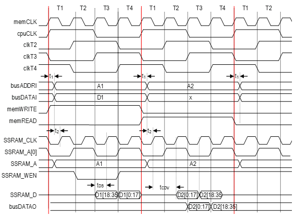
SSRAM Write Cycle followed by and Read Cycle
In read cycles, the SSRAM Write Enable (SSRAM_WE_N) is always negated.
In T1:
- At the beginning of T1, the FPGA asserts the address of the high-word of memory (DATA[0:17]) on the SSRAM Address Bus. SSRAM_A[0] is negated.
- At the middle of T1, the SSRAM device samples the address of the high-word from the SSRAM Address Bus.
In T2:
- At the beginning of T2, the FPGA asserts the address of the low-word of memory (DATA[18:35]) on the SSRAM Address Bus. SSRAM_A[0] is asserted.
- At the middle of T2, the SSRAM device samples the address of the low-word from the SSRAM Address Bus.
- At the middle of T2, the SSRAM drives the high-word of data (D[0:17]) onto the SSRAM Data bus.
In T3:
- At the beginning of T3, the FPGA captures the high-word of data (D[0:17]). SSRAM_A[0] is negated - but this is a "don't care" for read cycles.
- At the middle of T3, the SSRAM drives the low-word of data (D[18:35]) onto the SSRAM Data bus.
In T4:
- At the beginning of T4, the FPGA captures the high-word of data (D[18:35]). SSRAM_A[0] is asserted.
In T1:
- The FPGA speculatively starts a read cycle because it hasn't determined the cycle type before the beginning of T1. The data from this read cycle is eventually ignored. During T1, The FPGA determines that this is a write cycle and prepares for write operation in T2 and later.
- At the beginning of T1, the FPGA asserts the address of the high-word of memory (DATA[0:17]) on the SSRAM Address Bus. SSRAM_A[0] is negated.
- At the middle of T1, the SSRAM device samples the address of the high-word from the SSRAM Address Bus. Again, this is just speculation.
In T2:
- At the beginning of T2, the FPGA asserts the address of the low-word of memory (DATA[18:35]) on the SSRAM Address Bus. SSRAM_A[0] is asserted. Also, the FPGA asserts SSRAM Write Enable (SSRAM_WE_N) which facilitates writing to the low-word of memory.
- At the middle of T2, the SSRAM device samples the address of the low-word from the SSRAM Address Bus. Also the SSRAM drives the high-word of data (D[0:17]) onto the SSRAM Data bus. The data read from the FPGA was speculated incorrectly and is ignored by the FPGA.
In T3:
- At the beginning of T3, the FPGA asserts the address of the high-word of memory (DATA[0:17]) on the SSRAM Address Bus. SSRAM_A[0] is negated. Again, the FPGA asserts SSRAM Write Enable (SSRAM_WE_N) which facilitates writing to the high-word of memory. Lastly, the FPGA drives the low-word of memory (DATA[18:35]) on the SSRAM Data Bus.
- At the middle of T3, the SSRAM samples SSRAM_D[18:35].
In T4:
- At the beginning of T4, the FPGA asserts the address of the low-word of memory (DATA[18:35]) on the SSRAM Address Bus. SSRAM_A[0] is asserted. The FPGA negates SSRAM Write Enable which starts a dummy read cycle where the data will be available and ignored in the next T1. Lastly, the FPGA drives the high-word of memory (DATA[0:17]) on the SSRAM Data Bus.
- At the middle of T4, the SSRAM samples SSRAM_D[0:17].
From the description, you can observe that A0 is negated in T1, is asserted in T2, is negated in T3, and is asserted in T4. In other words, A0 just alternates.
It is also worth noting that the SSRAM is read high-word first because the read cycle starts in T1, while the SSRAM is written low-word first because the write cycle starts in T2.
This interface supports the older prototype board. It is not actively maintained.
The Xilinx Spartan 6 KS10 Memory Interface is design to accommodate a Cypress CY7C1460AV33 1M x 36-bit NoBL Pipelined Synchronous Static RAM (SSRAM).
This memory has a 2 stage pipeline between the address signals and the memory array. The device is capable of operating at a 166 MHz clock rate.
Because the memory device has a 2 stage pipeline, portions of the memory controller operate at four times the CPU clock rate. This creates the illusion that memory reads and memory writes complete in a single CPU clock cycle. For write operations the write enable signal (ssramWE_N) is asserted at the beginning (rising edge) of T2. The SSRAM device registers the address (ssramADDR[0:19]) and data (ssramDATA[0:35]) on the rising edge of the SSRAM Clock (ssramCLK). The write operation actually completes two clock cycles later at the beginning (rising edge) of T4. The address and data buses are generally unstable or contain the previous address and data during T1.
The memWRITE signal controls the SSRAM data bus interface direction. If the memWRITE signal is asserted, the FPGA asserts the busDATAI[0:35] signals onto the SSRAM data bus. If the memWRITE signal is negated, the FPGA tristates SSRAM data bus and the SSRAM data may be read from the SSRAM device.
In this mode, the SSRAM device will configure the direction of the SSRAM data bus based on the operation of the write enable signal (ssramWE_N). The data bus will be an output from the SSRAM except for two clock cycles after the write enable signal is asserted.
For reads, the address is sampled continuously but the memory device is enabled only in T4.

SSRAM Read Cycle

SSRAM Read Cycle Timing Parameters

SSRAM Write Cycle

SSRAM Write Cycle Timing Parameters
The Memory Controller and Memory is stable with no known deficiencies.
The diagnostic status of the KS10 memory controller (and memory) is summarized below:
                           DIAGNOSTIC                             RESULT
----------------------------------------------------------------  ------
DSMMAB0 DECSYSTEM 2020 KS10 1024K MEM DIAG . . . . . . . . . . .  Pass
DSMMBA0 DECSYSTEM 2020 BLT/FLOATING 1-0 MEMORY EXERCISER TEST  .  Pass
DSMMCB0 DECSYSTEM 2020 FAST AC DIAGNOSTIC  . . . . . . . . . . .  Pass
DSMMDC0 DECSYSTEM 2020 MEM DIAG  . . . . . . . . . . . . . . . .  Pass