Console Interface - KS10FPGA/KS10FPGA GitHub Wiki
At startup, the Intel Cyclone 5 Arm Cortex-A9 Hard Processor System (HPS) boots Ångström Linux as would any small system. The HPS hardware provides a 32-bit wide memory-mapped AXI4-Lite interface to the FPGA. The KS10 FPGA implements a similarly configured AXI4-Lite slave device which can receive AXI4 communications from the HPS.
Therefore, architecturally, the KS10 is a slave peripheral of the HPS system and all aspects of the KS10 are controlled by the HPS. This design echoes the design of the DEC KS10 where the Console Processor was a much less capable Intel 8080.
Beyond the obvious register interface, the interface should provide two interrupts from the KS10 to the console processor in order to handle asynchronous events.
In this system, The CTY either communicates with the console processor if the KS10 is halted or communicates with the KS10 if the KS10 is running. The best implementation of this has an interrupt that triggers any time that the KS10 run/halt status changes.
Also the characters from the KS10 to the CTY occur asynchronously. A second interrupt that indicates that a character is available would be nice but not mandatory.
For now, neither of these interrupts are present. The console processor creates a thread that polls the RUN/HALT state and polls for a character to be received. It is not the best implementation but it is acceptable.
As noted previously, the KS10 implements a mix of 32-bit, 36-bit, and 64-bit AXI4-Lite slave memory-mapped registers that that the HPS can access. These are:
Console Interface Register Inventory |
||||
Address |
Width |
Name |
Description |
|
0x00 |
36 |
Console Address Register |
||
0x08 |
36 |
Console Data Register |
||
0x10 |
36 |
Console Instruction Register |
||
0x18 |
32 |
Console Control/Status Register |
||
0x1c |
32 |
DZ11 Console Control Register |
||
0x20 |
32 |
LP20 Console Control Register |
||
0x24 |
32 |
RPxx Console Control Register |
||
0x28 |
32 |
MT Console Control Register |
||
0x2c |
32 |
DUP11 Console Control Register |
||
0x30 |
32 |
KMC11 Console Control Register (not implemented) |
||
0x34 |
32 |
- |
Reserved |
|
0x38 |
32 |
- |
Reserved |
|
0x3c |
32 |
- |
Reserved |
|
0x40 |
32 |
- |
Reserved |
|
0x44 |
32 |
- |
Reserved |
|
0x48 |
32 |
- |
Reserved |
|
0x4c |
32 |
- |
Reserved |
|
0x50 |
64 |
Instruction Trace Register |
||
0x58 |
64 |
PC and IR Registers |
||
0x60 |
64 |
MT Data Interface Register |
||
0x68 |
64 |
MT Debug Register |
||
0x70 |
64 |
RP Debug Register |
||
0x78 |
32 |
- |
Reserved |
|
0x7c |
32 |
- |
Reserved |
|
0x80 |
36 |
Breakpoint Address Register #0 |
||
0x88 |
36 |
Breakpoint Mask Register #0 |
||
0x90 |
36 |
Breakpoint Address Register #1 |
||
0x98 |
36 |
Breakpoint Mask Register #1 |
||
0xa0 |
36 |
Breakpoint Address Register #2 |
||
0xa8 |
36 |
Breakpoint Mask Register #2 |
||
0xb0 |
36 |
Breakpoint Address Register #3 |
||
0xb8 |
36 |
Breakpoint Mask Register #3 |
||
0xbc |
32 |
- |
Reserved |
|
0xc0 |
32 |
- |
Reserved |
|
0xc4 |
32 |
- |
Reserved |
|
0xc8 |
32 |
- |
Reserved |
|
0xcc |
32 |
- |
Reserved |
|
0xd0 |
32 |
- |
Reserved |
|
0xd4 |
32 |
- |
Reserved |
|
0xd8 |
32 |
- |
Reserved |
|
0xdc |
32 |
- |
Reserved |
|
0xe0 |
32 |
- |
Reserved |
|
0xe4 |
32 |
- |
Reserved |
|
0xe8 |
32 |
- |
Reserved |
|
0xec |
32 |
- |
Reserved |
|
0xf0 |
32 |
- |
Reserved |
|
0xf4 |
32 |
- |
Reserved |
|
0xf8 |
64 |
Firmware Version Register |
||
A few of these registers are recognizable to someone familiar with the DEC KS10. Most of them are modern additions that I've found useful enough to implement. These registers will be described in the following sections.
Note: A 64-bit aligned address space is reserved for each of the 36-bit register and each 36-bit register is right justified in that 64-bit address space.
The following sections detail the Console Interface register set.
The address that is used by the KS10 FPGA backplane bus is supplied by the Console Address Register.

Console Address Register (CONAR)
The address register definition is identical to the backplane bus definition that is described in Section 3.1, i.e., the bits of the Console Address Register are directly applied, 1:1, to the address bus of the backplane. This is illustrated below.

Console Address Register (CONAR) Bit Definitions
The Console Data Register is a 36-bit register that provides the data during a console-initiated memory or IO write transaction. The Console Data Register also receives the data that that is read during a console-initiated memory or IO read transaction.
Console Data Register (CONDR)
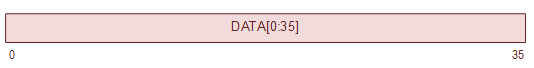
The Console Instruction Register is a 36-bit IO register located at IO Address o200000. After the KS10 Microcode initializes the KS10 micro-machine it fetches the contents of the Console Instruction Register and executes that instruction.
Normally this is a JRST instruction that jumps to the starting address of the boot loader or diagnostic code although the implementation places no constraints on the instruction that placed in this register. A JRST Instruction is opcode o254.
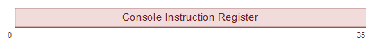
Console Instruction Register (CONIR)
The Console Control/Status Register is used to control the KS10 FPGA and to obtain status from the KS10 FPGA.

Console Control/Status Register (CONCSR)
Console Control/Status Register Definitions |
||||
Bit(s) |
Mnemonic |
R/W |
Init |
Description |
0-14 |
Reserved |
R |
- |
Reserved Writes ignored. Always read as zero. |
15 |
GO/BUSY |
R/W |
0 |
GO/Busy When GO is asserted, this bit starts a state-machine that performs a memory or IO transaction. BUSY (read) remains asserted until the memory or IO transaction is completed. When the bus transaction has completed, this bit will be negated automatically. Note: The Console Address Register and Console Data Register should not be modified when this bit is asserted. |
16-21 |
Reserved |
R |
- |
Reserved Writes ignored. Always read as zero. |
22 |
NXM/NXD |
R/W |
0 |
Non-existent Memory or Non-existent Device NXM/NXD is asserted if the last console-initiated bus transaction is not acknowledged by a memory or IO device. This bit is reset by writing a zero. |
23 |
HALT |
R |
- |
KS10 HALT Status Writes ignored. Halt is not RUN. |
24 |
RUN |
R/W |
0 |
KS10 Run Status When RUN is asserted, the KS10 will begin execution. When the RUN bit is negated, the KS10 will stop execution. The RUN bit is negated automatically by the KS10 microcode when a HALT condition occurs. See the section entitled "Controlling the KS10" for additional information about the RUN bit. |
25 |
CONT |
W |
0 |
KS10 KS10 Continue When CONT is asserted, the KS10 will exit the HALT state execute at least one instruction. The CONT bit is automatically cleared by the KS10 microcode once it is sampled and is always read as zero. See the section entitled "Controlling the KS10" for additional information about the CONT bit. |
26 |
EXEC |
W |
0 |
KS10 Execute When EXEC is asserted, the KS10 will exit the HALT State and execute the instruction in the Console Instruction Register (CONIR). The EXEC bit is automatically cleared by the KS10 microcode once it is sampled and is always read as zero. See the section entitled "Controlling the KS10" for additional information about the EXEC bit. |
27 |
TIMER EN |
R/W |
0 |
Timer Enable This bit enables the KS10 one millisecond interval timer. |
28 |
TRAP EN |
R/W |
0 |
Trap Enable This bit enables KS10 traps. |
29 |
CACHE EN |
R/W |
0 |
Cache Enable This bit enables the KS10 cache. |
30 |
KS10_INTR |
W |
0 |
This bit generates an interrupt from the Console to the KS10. Writing a ‘1’ will generate the interrupt; writing a '0' does nothing. This bit is always read as zero. |
31 |
KS10_RESET |
R/W |
1 |
When KS10_RESET is asserted, the KS10 is held in reset. KS10_RESET asserted (and the KS10 is held in reset) at power-up, otherwise KS10_RESET reflects the last value written. Note: The console microcontroller should initialize the most of the interface registers before negating the KS10_RESET signal. Note also: This does not reset any of the peripherals. |
The DZ11 Modem Control lines are not available external to the KS10 FPGA Board. The DZ11 Console Control Register is used to configure the DZ11 Modem Status register. It also controls the DZ11 loopback.

DZ11 Console Control Register (DZCCR)
DZ11 Console Control Register (DZCCR) Definition |
|||
Bit(s) |
Mnemonic |
R/W |
Description |
0-15 |
Reserved |
R/W |
Reserved Unused bits are read/write |
16-23 |
CO[7:0] |
R/W |
Carrier Sense These bits are reflected in the DZ11 Modem Status Register bits 15 through 8. |
24-31 |
RI[7:0] |
R/W |
Ring Indication These bits are reflected in the DZ11 Modem Status Register bits 7 through 0. |
The LP20 Console Control Register controls the interface between the KS10 and the serial printer. It also provides feedback on the number of line per inch and whether the printer is on-line. Lastly the operator can control whether the simulated printer has a optical vertical format unit or a digital (programmable) vertical format unit.
LP20 Console Control Register (LPCCR) Definitions |
|||||||
Bit(s) |
Mnemonic |
R/W |
Description |
||||
0-5 |
- |
R/W |
Unused. |
||||
6-10 |
SPEED |
R/W |
Baud Rate |
||||
0 |
50 Baud |
||||||
1 |
75 Baud |
||||||
2 |
110 Baud |
||||||
3 |
134.5 Baud |
||||||
4 |
150 Baud |
||||||
5 |
300 Baud |
||||||
6 |
600 Baud | ||||||
7 |
1200 Baud | ||||||
8 |
1800 Baud | ||||||
9 |
2000 Baud | ||||||
10 |
2400 Baud | ||||||
11 |
3600 Baud | ||||||
12 |
4800 Baud | ||||||
13 |
7200 Baud | ||||||
14 |
9600 Baud | ||||||
15 |
19200 Baud | ||||||
16 |
38400 Baud | ||||||
17 |
57600 Baud | ||||||
18 |
115200 Baud | ||||||
19 |
230400 Baud | ||||||
20 |
460800 Baud | ||||||
21 |
921600 Baud | ||||||
22-31 |
Reserved | ||||||
11-12 |
BITS |
R/W |
Number of Bits |
||||
0 |
5 Bits |
||||||
1 |
6 Bits |
||||||
2 |
7 Bits |
||||||
3 |
8 Bits |
||||||
13-14 |
PARITY |
R/W |
Parity Type |
||||
0 |
No Parity |
||||||
1 |
Odd Parity |
||||||
2 |
Even Parity |
||||||
3 |
Mark Parity |
||||||
15 |
STOP |
R/W |
Stop Bits |
||||
0 |
1 Stop Bit |
||||||
1 |
2 Stop Bits |
||||||
29 |
SIXLPI |
R |
LPI |
||||
0 |
8 LPI |
||||||
1 |
6 LPI |
||||||
30 |
OVFU |
R/W |
Vertical Formatting Unit |
||||
0 |
Digital Vertical Format Unit |
||||||
1 |
Optical Vertical Format Unit/p> |
||||||
31 |
ONLINE |
R/W |
Printer State |
||||
0 |
Printer Of-line |
||||||
1 |
Printer On-line |
||||||
The Magtape Console Control Register controls the status of the various TU-45 tape drives. Normally, these controls would be present on the tape drive but need to be emulated in this application.
Note: The format of this register is very similar to the RPCCR; but there are a few differences. The KS10 FPGA supports only a single TM03 Tape Control Unit (TCU), or formatter, which is Unit 0. The single TCU can support 8 slave drives.
MT Console Control Register (MTCCR) |
|||
Bit(s) |
Mnemonic |
R/W |
Description |
0-7 |
- |
R/W |
Reserved Unused. |
8 |
DPR[7] |
R/W |
Drive 7 Present |
9 |
DPR[6] |
R/W |
Drive 6 Present |
10 |
DPR[5] |
R/W |
Drive 5 Present |
11 |
DPR[4] |
R/W |
Drive 4 Present |
12 |
DPR[3] |
R/W |
Drive 3 Present |
13 |
DPR[2] |
R/W |
Drive 2 Present |
14 |
DPR[1] |
R/W |
Drive 1 Present |
15 |
DPR[0] |
R/W |
Drive 0 Present |
16 |
MOL[7] |
R/W |
Drive 7 Media On-line |
17 |
MOL[6] |
R/W |
Drive 6 Media On-line |
18 |
MOL[5] |
R/W |
Drive 5 Media On-line |
19 |
MOL[4] |
R/W |
Drive 4 Media On-line |
20 |
MOL[3] |
R/W |
Drive 3 Media On-line |
21 |
MOL[2] |
R/W |
Drive 2 Media On-line |
22 |
MOL[1] |
R/W |
Drive 1 Media On-line |
23 |
MOL[0] |
R/W |
Drive 0 Media On-line |
24 |
WRL[7] |
R/W |
Drive 7 Write Locked |
25 |
WRL[6] |
R/W |
Drive 6 Write Locked |
26 |
WRL[5] |
R/W |
Drive 5 Write Locked |
27 |
WRL[4] |
R/W |
Drive 4 Write Locked |
28 |
WRL[3] |
R/W |
Drive 3 Write Locked |
29 |
WRL[2] |
R/W |
Drive 2 Write Locked |
30 |
WRL[1] |
R/W |
Drive 1 Write Locked |
31 |
WRL[0] |
R/W |
Drive 0 Write Locked |
The RP Console Control Register controls the status of the various RP06 disk drives. Real RP06 disk drives provided controls are not emulated in the FPGA because of the SDHC media. These are:
RP Console Control Register (RPCCR) |
|||
Bit(s) |
Mnemonic |
R/W |
Description |
0-7 |
- |
R/W |
Reserved Unused. |
8 |
DPR[7] |
R/W |
Drive 7 Present |
9 |
DPR[6] |
R/W |
Drive 6 Present |
10 |
DPR[5] |
R/W |
Drive 5 Present |
11 |
DPR[4] |
R/W |
Drive 4 Present |
12 |
DPR[3] |
R/W |
Drive 3 Present |
13 |
DPR[2] |
R/W |
Drive 2 Present |
14 |
DPR[1] |
R/W |
Drive 1 Present |
15 |
DPR[0] |
R/W |
Drive 0 Present |
16 |
MOL[7] |
R/W |
Drive 7 Media On-line |
17 |
MOL[6] |
R/W |
Drive 6 Media On-line |
18 |
MOL[5] |
R/W |
Drive 5 Media On-line |
19 |
MOL[4] |
R/W |
Drive 4 Media On-line |
20 |
MOL[3] |
R/W |
Drive 3 Media On-line |
21 |
MOL[2] |
R/W |
Drive 2 Media On-line |
22 |
MOL[1] |
R/W |
Drive 1 Media On-line |
23 |
MOL[0] |
R/W |
Drive 0 Media On-line |
24 |
WRL[7] |
R/W |
Drive 7 Write Locked |
25 |
WRL[6] |
R/W |
Drive 6 Write Locked |
26 |
WRL[5] |
R/W |
Drive 5 Write Locked |
27 |
WRL[4] |
R/W |
Drive 4 Write Locked |
28 |
WRL[3] |
R/W |
Drive 3 Write Locked |
29 |
WRL[2] |
R/W |
Drive 2 Write Locked |
30 |
WRL[1] |
R/W |
Drive 1 Write Locked |
31 |
WRL[0] |
R/W |
Drive 0 Write Locked |
The DUP11 device is still in-work even though it passes many of its diagnostic tests.
The idea here is that the DUP11 will expose a Transmitter FIFO and a Receiver FIFO to the HPS that will forward data packets via Ethernet.
DUP11 Console Control Register (DUPCCR) Definition |
|||
Bit(s) |
Mnemonic |
R/W |
Description |
0 |
Reserved |
R/W |
Reserved Unused bits are read/write |
1 |
TXE |
R |
Transmitter FIFO empty |
2-3 |
- |
R/W |
Reserved Unused bits are read/write. |
4 |
RI |
R/W |
Ring indication |
5 |
CTS |
R/W |
Clear to Send |
6 |
DSR |
R/W |
Data Set Ready |
7 |
DCD |
R/W |
Data Carrier Detect |
8-15 |
TXFIFO |
R |
Transmitter FIFO |
16 |
RXF |
R |
Receiver FIFO Full |
17 |
DTR |
R |
Data terminal ready |
18 |
RTS |
R |
Request to send |
20 |
H325 |
R/W |
Install H325 Loopback Plug |
21 |
W3 |
R/W |
Install W3 Jumper Plug |
22 |
W5 |
R/W |
Install W5 Jumper Plug |
23 |
W6 |
R/W |
Install W6 Jumper Plug |
24-31 |
RXFIFO |
R/W |
RXFIFO Interface |
The Breakpoint Facility monitors the address on the KS10 Backplane Bus and halts the KS10 CPU when the “Address Match” conditions are met.
The Breakpoint Address Register are a set of 36-bit registers that sets the breakpoint address. The Breakpoint Mask Register is another set of 36-bit registers that controls which bits of the Breakpoint Address are used in the breakpoint comparison and which bits are ignored.
It should be noted that the Breakpoint Register examines the KS10 Backplane and therefore operates on Physical Addresses and not on Virtual Addresses. Also, the breakpoint facility will only breakpoint on addresses generated by the CPU. It will not breakpoint on DMA operations.
In actual implmentation, there are 4 sets of breakpoint registers, BRAR[0:3] and BRMR[0:3]. BRAR[0] and BRMR[0] are paired together. Likewise, BRAR[1] and BRMR[1] are paired together, etc.
Because the KS10 backplane implementation has both a READ bit and a WRITE bit associated with the address, a naive breakpoint implementation could not break on either reads or writes - it could only breakpoint on reads and breakpoint on writes. The KS10 FPGA actually implements two address comparisons for each breakpoint register: one address comparison for reads and one address comparison for writes. Therefore for this implementation allows breakpoint on reads or breakpoint on writes.
It goes without saying that there are a lot of bus-cycles that could be detected with the breakpoint system that are not really useful.
The Breakpoint Address Register is illustrated below:

Breakpoint Address Register (BRAR[0:3])
The bit definitions of the Breakpoint Address Register Definition is illustrated below:
Breakpoint Address Register (BRAR[0:3]) Definitions |
||||
Bit(s) |
Mnemonic |
R/W |
Description |
|
0-13 |
FLAGS |
R/W |
FLAGS |
|
0 |
User Mode |
|||
1 |
Not used |
|||
2 |
Fetch Cycle |
|||
3 |
Read Cycle |
|||
4 |
Write Test Cycle |
|||
5 |
Write Cycle |
|||
6 |
Extended Cycle |
|||
7 |
Cache Enabled |
|||
8 |
Physical Address |
|||
9 |
PCXT |
|||
10 |
IO Cycle |
|||
11 |
IO Who Are You Cycle |
|||
12 |
IO Interrupt Cycle |
|||
13 |
IO Byte Cycle |
|||
14-35 |
ADDRESS |
R/W |
ADDRESS |
|
The Breakpoint Mask Register(s) (BRMR) provides a mechanism to include or ignore the various address and flag bits that are associated with the Backplane. When a bit is asserted in the BRMR, the associated bit in the Breakpoint Address Register (BRAR) will be included in the breakpoint comparison. When the bit is negated in the BRMR, the bit will be ignored in the breakpoint comparison.
Note: If the READ bit in the BRMR is set, the breakpoint system will breakpoint only on reads. If the WRITE bit in the BRMR is set, the breakpoint system will breakpoint on only writes. If both the READ and WRITE bits in the BRMR are both set, the breakpoint will trigger on either reads or writes.
The Breakpoint Mask Register (BRMR[0:3])is illustrated below:

Breakpoint Mask Register
The bit definitions of the Breakpoint Mask Register (BRMR[0:3]) Definition is illustrated below:
Breakpoint Mask Register (BRMR[0:3]) Definitions |
||||
Bit(s) |
Mnemonic |
R/W |
Description |
|
0-13 |
FLAGS |
R/W |
FLAGS |
|
0 |
User Mode |
|||
1 |
Not used |
|||
2 |
Fetch Cycle |
|||
3 |
Read Cycle |
|||
4 |
Write Test Cycle |
|||
5 |
Write Cycle |
|||
6 |
Extended Cycle |
|||
7 |
Cache Enabled |
|||
8 |
Physical Address |
|||
9 |
PCXT |
|||
10 |
IO Cycle |
|||
11 |
IO Who Are You Cycle |
|||
12 |
IO Interrupt Cycle |
|||
13 |
IO Byte Cycle |
|||
14-35 |
ADDRESS |
R/W |
ADDRESS |
|
The Instruction Trace Register allows certain CPU registers to be stored as program execution occurs. As the program executes, the Program Counter (PC) and the Instruction Register (IR) is stored in the Trace Buffer when an instruction is executed.
The Trace Buffer is a simple stack. When the most significant word (bits 0-15) of the Instruction Trace Register is read, the buffer state is updated.
The Instruction Trace Register is defined below:

Instruction Trace Register
Instruction Trace Register (ITR) Definitions |
|||
Bit(s) |
Mnemonic |
R/W |
Description |
0 |
CLR |
W |
Clear Asserting CLR will reset the trace buffer. When this occurs, FULL is negated and EMPTY is asserted. Always read as zero. |
1 |
FULL |
R |
Buffer Full Full is asserted when the buffer is full. Full is negated by asserting CLR. Writes ignored. |
2 |
EMPTY |
R |
Buffer Empty Empty is asserted when the buffer is empty. Empty is asserted by asserting CLR. Writes ignored. |
3-7 |
SIZE[4:0] |
R |
Buffer Size The trace buffer size is parameterized. The buffer size is fixed when the FPGA is built. This field reports the actual log2(buffer_size) as implemented in the FPGA. In other words, if the trace buffer size is 4096 entries, this field reports 12. |
8-9 |
- |
R |
Reserved Writes ignored. Always read as zero. |
10-27 |
PC[18:35] |
R |
Program Counter Writes ignored. The PC register contains the captured value Program Counter. |
28-63 |
IR[0:35] |
R |
Instruction Register Writes ignored. The IR register contains the captured value of the Instruction Register. |
Sometimes it's nice just to know what is happening and what code is executing. Typing a ^T on the CTY when the KS10 is executing will capture the PCIR register and print the captured, disassembled instruction on the CTY.
The Program Counter and Instruction Register is defined below:
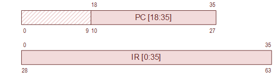
Program Counter and Instruction Register
Program Counter and Instruction Register (PCIR) Definitions |
|||
Bit(s) |
Mnemonic |
R/W |
Description |
0-9 |
- |
R/W |
Reserved Writes ignored.Always read as zero. |
10-27 |
PC[18:35] |
R |
Program Counter Writes ignored.The PC register is loaded with the last value of the Program Counter. |
28-63 |
IR[0:35] |
R |
Instruction Register The IR register is loaded with the last value of the Instruction Register. |
This register is the interface between the Console Processor and the MT Tape Controller.
MT Data Interface Register (MTDIR) |
||||
Bit(s) |
Mnemonic |
R/W |
Description |
|
63 |
READ |
R |
Tape Read Mode READ is deprecated and should be ignored. |
|
62 |
STB |
R/W |
Strobe During read functions, the console processor will provide tape data from a file to the Tape Controller by asserting data onto the DATA bits and then asserting STB. Alternately STB and DATA can be asserted simultaneously in a single atomic 64-bit write operation, if that can be guaranteed. In this case, the Tape Controller automatically negates the STB signal once the data has been read. In read mode, the console processor cannot negate the STB signal once asserted. Note: Read functions include Read Forward, Read Reverse, Write Check Forward, and Write Check Reverse. During write functions, the Tape Controller will provide data to the console processor to write to a file, by asserting STB and asserting data on the DATA bits. When the console processor has read the data it should negate the STB signal. DATA should be ignored if STB is negated. In write mode, The console processor cannot assert STB. Note: The only write function is Write Forward. |
|
61 |
INIT |
R |
Initialize INIT is deprecated and should be ignored. |
|
60 |
READY |
R/W |
Ready The Tape Controller in the FPGA negates the READY bit to notify the console software to process a command. When the console software has completed the command, it asserts READY. Note: the console processor can only assert the READY bit. It cannot negate the READY bit. The MTDS[DRY] bit reflects the state of this bit. The MTCS1[GO] bit reflects the negated state of this bit. |
|
59 |
INCFC |
W |
Increment Frame Counter The console processor should assert INCFC to notify the tape controller to increment the Frame Counter. The tape controller automatically negates the INCFC bit when the Frame Counter has been incremented. Negating the INCFC bit has no effect. Always read as zero. |
|
58-56 |
SS[2:0] |
R |
Slave select Writes ignored. SS reflects the contents of the MTTC[SS] register. |
|
55-53 |
DEN[2:0] |
R |
Density Writes ignored. DEN reflects the contents of the MTTC[DEN] register. |
|
52-48 |
FUN[4:0] |
R |
Function Writes ignored. FUN reflects the contents of the MTCS1[FUN] register. |
|
47-44 |
FMT[3:0] |
R |
Format Writes ignored. FMT reflects the contents of the MTTC[FMT] register. |
|
43 |
WCZ |
R |
Word Count is Zero Writes ignored. WCZ is asserted when the contents of the Word Count Register is zero. |
|
42 |
FCZ |
W |
Frame Count is Zero Writes ignored. FCZ is asserted when the contents of the Frame Count Register is zero. |
|
41 |
SETBOT |
W |
Set Beginning-of-Tape When SETBOT is asserted, the Beginning-of-Tape indication (MTDS[BOT]) will be asserted. Negating the SETBOT bit has no effect. Always read as zero. |
|
40 |
CLRBOT |
W |
Clear Beginning-of-Tape When CLRBOT is asserted, the Beginning-of-Tape indication (MTDS[BOT]) will be negated. Negating the CLRBOT bit has no effect. Always read as zero. |
|
39 |
SETEOT |
W |
Set End-of-Tape When SETEOT is asserted, the End-of-Tape indication (MTDS[EOT]) will be asserted. Negating the SETEOT bit has no effect. Always read as zero. |
|
38 |
CLREOT |
W |
Clear End-of-Tape When CLREOT is asserted, the End-of-Tape indication (MTDS[EOT]) will be negated. Negating the CLREOT bit has no effect. Always read as zero. |
|
37 |
SETTM |
W |
Set Tape Mark When SETTM is asserted, the Tape Mark indication (MTDS[TM]) will be asserted. Negating the SETTM bit has no effect. Always read as zero. |
|
36 |
CLRTM |
W |
Clear Tape Mark When CLRTM is asserted, the Tape Mark indication (MTDS[TM]) will be negated. Negating the CLRTM bit has no effect. Always read as zero. |
|
35-0 |
DATA[0:35] |
R/W |
Tape Data See operation of the STB bit above for a description of how to read and write to the DATA bits. During read operations, DATA is write-only. During write operations, DATA is read-only. The console processor performs all of the tape formatting which involves translating bytes on the tape into 36-bit PDP-10 words and vice-versa. The console processor supports the same formats that the DEC TM03 supports. Note: There is an endian swap in this register. |
|
The MT Debug Register is a register that is not present on a DEC KS10. It is present only to facilitate debugging the KS10 FPGA MT Tape Controller

MT Debug Register
The bit definitions of the MT Debug Register is defined below.
MT Debug Register Definitions |
|||
Bit(s) |
Mnemonic |
R/W |
Description |
0-7 |
STATE |
R |
Tape Controller State Machine State STATE contains the current state of the Tape Controller State Machine. |
8-15 |
- |
R |
Reserved |
16-23 |
- |
R |
Reserved |
24-31 |
- |
R |
Reserved |
32-47 |
WRCNT |
R |
Number of Disk Writes This is a 16-bit counter that is incremented on each write operation. |
48-63 |
RDCNT |
R |
Number of Disk Reads This is a 16-bit counter that is incremented on each read operation. |
The RP Debug Register is a register that is not present on a DEC KS10. It is present only to facilitate debugging the KS10 FPGA RP Disk Controller. The FPGA design makes it difficult to probe inside the RP06 controllers to get status. This register also provides Disk Drive blinking lights.

RP Debug Register
The bit definitions of the RP Debug Register is defined below.
RP Debug Register Definitions |
|||
Bit(s) |
Mnemonic |
R/W |
Description |
0-7 |
STATE |
R |
SDHC Card State Machine State STATE contains the current state of the State Machine that manages the interface to the SD Card. |
8-15 |
ERRNUM |
R |
Error Number When the State Machine detects an issue with the SD Card interface, the State Machine records ERRNUM which uniquely describes the circumstances of the failure. |
16-23 |
ERRVAL |
R |
Error Value When the State Machine detects an unexpected or incorrect response from the SD Card, the State Machine records response of the SD Card in ERRVAL. |
24 |
DISK0 |
R |
Disk 0 Activity LED |
25 |
DISK1 |
R |
Disk 1 Activity LED |
26 |
DISK2 |
R |
Disk 2 Activity LED |
27 |
DISK3 |
R |
Disk 3 Activity LED |
28 |
DISK4 |
R |
Disk 4 Activity LED |
29 |
DISK5 |
R |
Disk 5 Activity LED |
30 |
DISK6 |
R |
Disk 6 Activity LED |
31 |
DISK7 |
R |
Disk 7 Activity LED |
32-47 |
WRCNT |
R |
Number of Disk Writes This is a 16-bit counter that is incremented on each write operation. |
48-63 |
RDCNT |
R |
Number of Disk Reads This is a 16-bit counter that is incremented on each read operation. |
The Firmware Version Register is used for basic diagnostics and to allow the console to print the firmware revision of the FPGA.
One of the first tests that the console will perform is to attempt to read the contents of the Firmware Version Register from the FPGA. If the result is not consistent with the expected results, the console will print an error message and not attempt to boot the KS10 processor.
This test verifies that the FPGA is programmed and that there is a working bus connection between the console microcontroller and the FPGA.
The format of the Firmware Version Register is summarized below.

Firmware Version Register
The bit definitions of the Firmware Version Register is defined below.
Console Firmware Version Register Definitions |
||||
Byte |
Value |
ASCII |
R/W |
Description |
0 |
0x52 |
'R' |
R |
Always 'R' |
1 |
0x45 |
'E' |
R |
Always 'E' |
2 |
0x56 |
'V' |
R |
Always 'V' |
3 |
* |
* |
R |
Major Revision MS Byte |
4 |
* |
* |
R |
Major Revision LS Byte |
5 |
0x2e |
'.' |
R |
Always '.' |
6 |
* |
* |
R |
Minor Revision MS Byte |
7 |
* |
* |
R |
Minor Revision LS Byte |
|
* Contents depend of firmware revision which is built into the firmware. When printed, the firmware version register looks something like "REV23.45" |
||||
This section describes the signals that are generated by the Console Microcontroller that control the operation of the KS10.
The RUN bit, the CONT bit, and the EXEC
bit control the KS10 operation as illustrated below:

KS10 Control State Diagram
When in the HALT State, the table below enumerates the types of
operations that the KS10 will perform when the control bits are set in the
various states.
KS10 Control Operation |
|||
CONT |
EXEC |
RUN |
Operation |
0 |
X |
X |
Remain in HALT State |
1 |
0 |
0 |
Execute the single instruction at current PC (i.e., single step) |
1 |
0 |
1 |
Continue execution at current PC |
1 |
1 |
0 |
Execute the single instruction in the Console Instruction Register |
1 |
1 |
1 |
Begin execution with the instruction in the Console Instruction Register |
The operation of these bits is also detailed in the following sections.
The RUN bit controls whether the KS10 is in the
RUN State or HALT State.
Setting the RUN bit will allow the KS10 to execute one or more
instructions. The RUN bit is examined by the microcode at the end of each
instruction.
When the RUN bit is asserted, the KS10 will execute the next
instruction.
When the RUN bit is cleared, the KS10 will finish the current
instruction and enter the Halt State.
When the KS10 is in the HALT State, setting the
CONT bit will cause the KS10 to exit the HALT State
and execute at least one instruction. At the end of that instruction, the
RUN bit is examined.
If the RUN bit is asserted, the KS10 will continue to execute
instructions.
If the RUN bit is negated, the KS10 will re-enter the
HALT State - essentially single-stepping the processor.
When the KS10 is in the HALT State, setting the CONT
bit and EXEC bit will cause the KS10 to exit the
HALT State and execute the instruction in the Console Instruction
Register (CIR). At the end of that instruction, the RUN bit is
examined.
If the RUN bit is asserted, the KS10 will continue to execute
instructions. This technique is used by the Console at startup to cause the
KS10 to begin executing the boot loader or diagnostic program at a specific
address. In this case, a JRST instruction which performs a jump to the starting
address of the boot loader is placed into the Console Instruction Register.
If the RUN bit is negated, the KS10 will re-enter the
HALT State - essentially executing the single instruction in the
Console Instruction Register (CIR).
The Console Communications Area is a region of KS10 memory that is accessible by both the KS10 and the Console Processor. This memory is used to communicate between the two devices.
Most of the information in this section is not very well documented. It has mostly been obtained by reading the monitor source code and reading the I8080 "microcode".
KS10/Console Communications Area |
||
Address |
Value |
Summary |
000030 |
000000_000000 |
The Halt Switch memory location is used by the console processor to shutdown or restart the monitor program. |
000031 |
003740_000000 |
The Keep Alive memory location is used by the console processor to periodically check the status of the monitor program executing in the KS10 and take action (reboot) if necessary. The console processor can also interact with the monitor program at startup so that the reason for the reboot is captured in the log files. |
000032 |
This memory location contains the CTY Input Word. This is used to send characters from the console processor to the KS10. |
|
000033 |
This memory location contains the CTY Output Word. This is used by the KS10 to send characters to the console processor. |
|
000034 |
KLINIK Input Word. KLINIK is not implemented. |
|
000035 |
KLINIK Output Word. KLINIK is not implemented. |
|
000036 |
RP Disk: 1776700 MT Tape: 3772440 |
This memory location contains to address of the RH11 Massbus Controller for the boot device. The RH11 address includes the UBA number. |
000037 |
This memory location contains the unit number of the boot device. |
|
000040 |
000000_002000 |
This memory location contains the magtape parameters of the boot device. The contents of this memory location is used to set the MT Tape Control Register (MTTC) if the boot device is a magtape. If the boot device is a disk drive, this parameter is ignored. |
Halt Switch (KS10 Memory Address 000030) |
||
Bit(s) |
Mnemonic |
Description |
0-35 |
HALT |
Halt Switch This register is initialized to zero at startup. The console processor can request that the monitor shut itself down by storing a non-zero value to this location. If the value written is the base address of the RH11 disk controller (01776700) the monitor will reboot. |
The Keep Alive Word bits-fields are aligned on bytes because of the i8080 interface. The i8080 has a 32-bit interface to this 36-bit memory location.
Bits 0-3 are not accessed by the i8080.
Bits 4-11 (Byte 0) are configuration bits.
Bits 12-19 (Byte 1) are also configuration bits.
Bits 20-27 (Byte 2) is the keep alive byte.
Bits 28-35 (Byte 3) are the "Why reload?" bits.
Keep Alive Word (KS10 Memory Address 000031) |
||
Bit(s) |
Mnemonic |
Description |
0-3 |
- |
Reserved |
4 |
KSRLD |
Reload Request The KS10 asserts this bit to ask the console processor to reload the KS10. When this occurs, the console processor will:
|
5 |
KPACT |
Keep Alive Active The console processor will reload the KS10 if this is asserted and KPALIV does not change. The KS10 increments the KPALIV field every second and the console processor periodically checks the KPALIV bits. If the console processor does not detect a change in the KPALIV field after 15 seconds, the console processor will reboot the KS10. When this occurs, the console processor will:
|
6 |
KLACT |
KLINIK Active KLINIK is not implemented. |
7 |
PAREN |
Memory Parity Error Detect Enabled The console processor normally sets PAREN at startup. The KS10 FPGA doesn't implement parity so this has no effect. |
8 |
CRMPAR |
CRAM Parity Error Detect Enabled The console processor normally sets CRMPAR at startup. The KS10 FPGA doesn't implement parity so this has no effect. |
9 |
DRMPAR |
DRAM Parity Error Detect Enabled The console processor normally sets DRMPAR at startup. The KS10 FPGA doesn't implement parity so this has no effect. |
10 |
CASHEN |
Cache Enabled The console processor normally sets CASHEN at startup. |
11 |
MILSEN |
1 Millisecond Timer Enabled The console processor normally sets MILSEN at startup. |
12 |
TRPENA |
Traps Enabled The console processor normally sets TRPENA at startup. |
13 |
MFGMOD |
Manufacturing Mode The console processor always sets this to zero. |
14-19 |
- |
Reserved Reserved bits should be set to zero. |
20-27 |
KPALIV |
Keep Alive When operating properly, the KS10 increments KPALIV every second. See description of KPACT above for more information. |
28-32 |
- |
Reserved Reserved bits should be set to zero. |
32 |
AUTOBT |
Auto boot AUTOBT is asserted by the console processor at startup or when the boot switch is activated. The monitor uses this bit to log why the startup is occurring. |
33 |
PWRFAL |
Power Fail Restart PWRFAL is asserted by the console processor before a startup that was caused by a power failure. The monitor uses this bit to log why the startup is occurring. The KS10 FPGA doesn't implement power fail. It looks like the KS10 didn't support power fail either. The comments for the Version 5.2 I8080 microcode states: (5.2G) THIS CODE WAS FOR HANDLING POWER FAIL RESTART WITH BATTERY BACKUP.
SINCE THERE IS NO BATTERY BACKUP ANY MORE, IT IS TAKEN OUT.
|
34 |
FORREL |
Forced Reload FORREL is asserted by the console processor before a startup that was caused by a reload request. The monitor uses this bit to log why the startup is occurring. The misnomer "Forced Reload" is inconsistently applied to this bit |
35 |
KEPFAL |
Keep alive failure KEPFAL is asserted by the console processor before a startup that was caused by a keep-alive failure. The monitor uses this bit to log why the startup is occurring. |
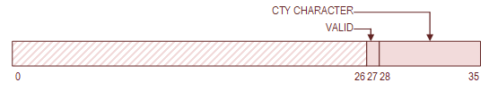
The CTY input protocol uses KS10 memory location 000032 to transfer the CTY character plus a 1-bit flag (Valid) from the Console Processor to the KS10.
This is illustrated below:

KS10 CTY Input Word (KS10 Memory Address 000032)
KS10 CTY Output Word (KS10 Memory Address 000032) |
||
Bit(s) |
Mnemonic |
Description |
0-26 |
Reserved |
Ignored for reads and writes. |
27 |
VALID |
Asserted by Console Processor when character is available for the KS10 to read. Cleared by the KS10 after the character has been read. |
28-35 |
CTY Character |
ASCII Character. Asserted by Console Processor when character is available for the KS10 to read. Cleared by the KS10 after the character has been read. |
The procedure from transferring a character from the Console Processor to the KS10 is as follows:
- The Console Processor verifies that there is no character already in the buffer to the KS10 by checking the VALID bit of location 000032. If the VALID bit it is still set, the Console Processor should wait until later.
- The Console Processor places a character with the VALID bit set in memory location 0000032.
- The Console Processor Interrupts the KS10 by setting the KS10_INTR bit in the Console Control/Status Register.
The CTY Input Word should be initialized to zero by the Console Processor before starting the KS10.
The CTY output protocol uses KS10 memory location 000033 to transfer the CTY character plus a 1-bit flag (Valid) from the KS10 to the Console Processor.
This is illustrated below:
KS10 CTY Output Word (KS10 Memory Address 000033)
KS10 CTY Output Word (KS10 Memory Address 000032) |
||
Bit(s) |
Mnemonic |
Description |
0-26 |
Reserved |
Ignored for reads and writes. |
27 |
VALID |
Asserted by KS10 when character is available for the Console to read. Cleared by the Console after the character has been read. |
28-35 |
CTY Character |
ASCII Character. Asserted by KS10 when character is available for the Console to read. Cleared by the Console after the character has been read. |
The procedure for transferring a character from the KS10 to the Console is a follows:
- The KS10 places a character with the VALID bit set in memory location 0000032.
- The KS10 interrupts the Console Processor.
- The Console Processor is interrupted.
- If the VALID bit is asserted, the Console Processor extracts the character from location 000032 bits 28-35 and outputs the character on the CTY serial output port. If the VALID bit is negated, the interrupt function should not process a character from the KS10. Note: the interrupt may indicate that another character should be transferred to the KS10.
- The Console Processor zeros location 000032. This zeros the VALID bit.
- The Console Processor Interrupts the KS10 by setting the KS10_INTR bit in the Console Control/Status Register.
The CTY Output Word should be initialized to zero by the Console Processor before starting the KS10.
KS10 KLINIK Input Word (KS10 Memory Address 000034) |
|||
Bit(s) |
Mnemonic |
Description |
|
0-25 |
Reserved |
Ignored for reads and writes. |
|
26-27 |
KLCHR |
Meaning: |
|
KLCHR[1:0] |
Description |
||
0 |
Nothing |
||
1 |
Character Available |
||
2 |
KLINIK Initialized |
||
3 |
Carrier Lost |
||
28-35 |
KLIICH |
KLINIK character (ASCII). |
|
KS10 KLINIK Output Word (KS10 Memory Address 000035) |
||
Bit(s) |
Mnemonic |
Description |
0-25 |
Reserved |
Ignored for reads and writes. |
26 |
KLHUP |
KLINIK hang-up request |
27 |
VALID |
KLINIK character available |
28-35 |
KLIICH |
KLINIK character (ASCII). |
KS10 RH11 Address Word (KS10 Memory Address 000036) |
||
Bit(s) |
Mnemonic |
Description |
0-13 |
Reserved |
Ignored for reads and writes. |
14-35 |
ADDR |
RH11 Base Address (including UBA). |
KS10 KLINIK Input Word (KS10 Memory Address 000034) |
|||
Bit(s) |
Mnemonic |
Description |
|
0-32 |
Reserved |
Ignored for reads and writes. |
|
33-35 |
UNIT |
Unit Select |
|
UNIT[2:0] |
Description |
||
0 |
Device 0. |
||
1 |
Device 1. |
||
2 |
Device 2. |
||
3 |
Device 3. |
||
4 |
Device 4. |
||
5 |
Device 5. |
||
6 |
Device 6. |
||
7 |
Device 7. |
||
This 36-bit parameter gets copied (right justified) to a 16-bit Magtape Tape Control (MTTC) Register. It allows the operator to set the Tape Format, Tape Density, and Tape Transport (Slave Unit).
KS10 Boot Magtape Parameter Word (KS10 Memory Address 000040) |
|||
0-24 |
- |
Reserved Ignored. |
|
25-27 |
DEN[2:0] |
Density Select |
|
DEN[2:0] |
Description |
||
0 |
Format Unknown. |
||
1 |
800 BPI NRZ. |
||
2 |
Format Unknown. |
||
3 |
800 BPI NRZ. |
||
4 |
1600 BPI PE. |
||
5 |
Format Unknown. |
||
6 |
Format Unknown. |
||
7 |
Format Unknown. |
||
28-31 |
FMT[3:0] |
Format Select |
|
FMT[3:0] |
Description |
||
0 |
PDP-10 Core Dump 4x 8-bit characters plus 1x 4-bit character |
||
1 |
PDP-15 Core Dump 3x 6-bit characters. |
||
3 |
PDP-10 Normal 4x 8-bit characters. |
||
12 |
PDP-11 Normal 2x 8-bit characters. |
||
13 |
PDP-11 Core Dump 4x 4-bit characters. |
||
14 |
PDP-15 Normal 2x 8-bit characters. |
||
32 |
- |
Reserved Ignored. |
|
33-35 |
SS[2:0] |
Slave Select Specifies the unit number of the tape transport. |
|
The Console Interface is stable with no known deficiencies.
The diagnostic status of the KS10 Console Interface is summarized below:
                           DIAGNOSTIC                            Result
---------------------------------------------------------------- ------
DSLTA   DECSYSTEM 2020 TELETYPE TEST . . . . . . . . . . . . . . Pass