DIY ATtiny HV UPDI Programmer - Dlloydev/jtag2updi GitHub Wiki
The firmware here supports using an ATtiny1604, 1614, 1606, 1616, 3216, 1607, 1617 or 3217 as a HV UPDI programmer. Just use a breakout board or development board for the host MCU. If you use any 5V USB serial adapter or IC with an RTS or DTR signal, an auto reset circuit and use a bootloader option in megaTinyCore, you'll be able to use the ATtiny HV programmer like a regular Arduino board to upload sketches to the target or update the programmer's firmware.
| Click image to enlarge |
|---|
|
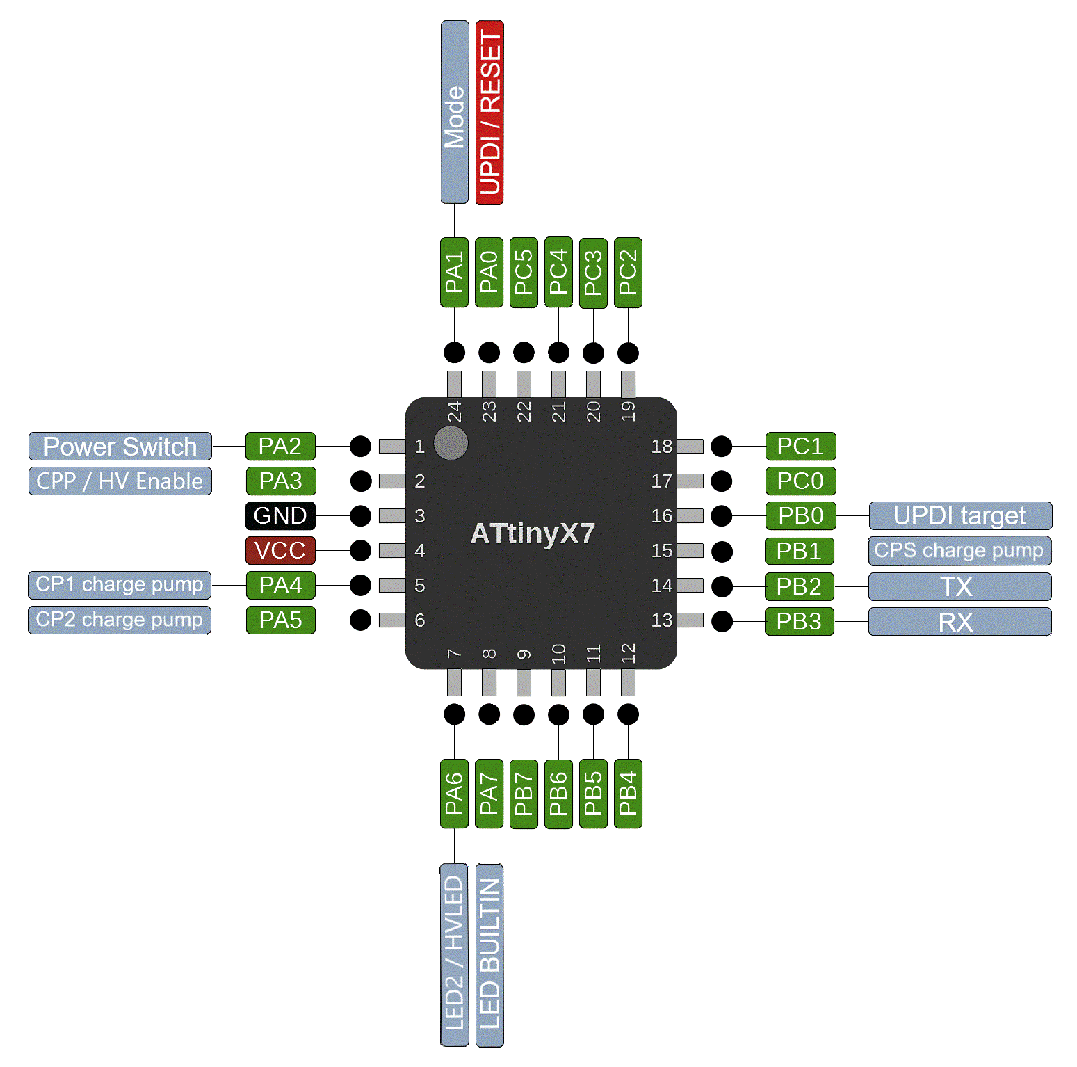 |
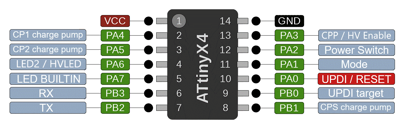
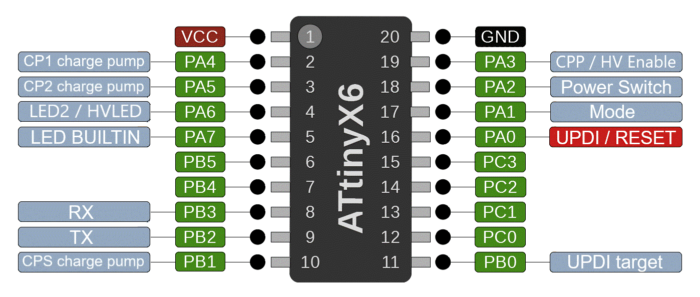
| Pin | Name | Type | Description |
|---|---|---|---|
| PA0 | UPDI/RESET | Bidirectional/Input | Factory UPDI programming and Reset input, pullup enabled |
| PA1 | Mode | Input | Mode selection, 8-bit ADC, floating input |
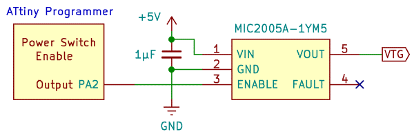
| PA2 | Power Switch | Output | Enable for power switch controlling target power cycle, active high |
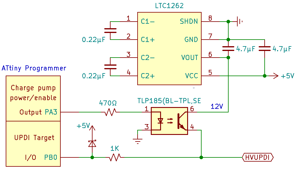
| PA3 | CPP/HV Enable | Output | Charge pump power, normally low, high during HV UPDI enable pulse |
| PA4 | CP1 charge pump | Output | Charge pump Clock 1, 413kHz during UPDI enable |
| PA5 | CP2 charge pump | Output | Charge pump Clock 2, 413kHz during UPDI enable |
| PA6 | LED2/HVLED | Output | Used to indicate NVM version or UPDI enable 12V pulse |
| PA7 | LED BUILTIN | Output | Active during programming and pulses upon release of reset |
| PB0 | UPDI target | Bidirectional | Target UPDI programming |
| PB1 | CPS charge pump | Output | Charge pump shutdown, normally high, low during UPDI enable pulse |
| PB2 | TX | Output | USB to serial communication to PC, TTL logic levels |
| PB3 | RX | Input | USB to serial communication to PC, TTL logic levels |
| Item | Qty | Part Number | Description |
|---|---|---|---|
| 1 | 1 | ATtiny1614/1604 dev board | Arduino compatible development/breakout board with optiboot and auto-reset circuit. |
| 2 | 1 | Serial Adapter | Serial adapter (5V) with DTR or RTS signal |
| 3 | 1 | Arduino Nano HV UPDI Programmer PCB for tinyAVR 0/1 | Circuit board providing 12V charge pump circuit, HV LED, mode select jumper (3 modes) and 3-pin target UPDI interface. |
| 4 | 1 | MIC2005A-1YM5 | High-side power switch, active high enable (requires SOT23-5 adapter) |
No full schematic provided as you may want to create your own custom board or prototype. Refer to the schematics and datasheets provided with your chosen components.
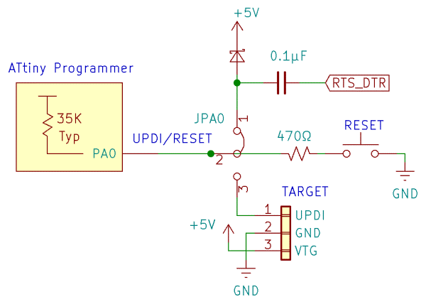
| JPA0 | FUNCTION |
|---|---|
| REMOVED | Normal operation for uploading sketches to the target. |
| 1-2 | The RTS/DTR auto-reset circuit is connected. Used when updating firmware using a serial connection. |
| 2-3 | Used when updating firmware with another HV UPDI programmer. |
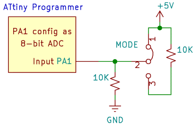
| Jumper | Mode | PA0 Configurations | HV Pulse | Power Cycle |
|---|---|---|---|---|
| REMOVED (GND) | UPDI | UPDI | NO | NO |
| 2-3 (2.5V) | HV | UPDI, RESET | YES | NO |
| 1-2 (5V) | PCHV | UPDI, RESET, GPIO | YES | YES |
For 12V power, a charge pump IC can free up a few pins on the programmer. An alternative method would be using a switching DC-DC boost converter.
A high side power switch IC could be used for target power cycle. An alternative method would be using a high side MOSFET switching circuit.
-
Install megaTinyCore
-
In "Tools", select the board with optiboot option, chip, port, programmer and configure the UPDI pin as Reset.
-
Since this is a first time installation of the bootloader, remove the FW jumper. Now use a HV UPDI Programmer connected directly to PA0, VCC and GND and "Burn Bootloader".
-
Reinstall the FW jumper and connect serial RX, TX and RTS/DTR signals to the programmer's MCU.
-
Now you can use the serial port to Install the HV Programmer Firmware
● Click on the green "Clone or download" button, then select "Download ZIP".
● Unzip this file in a folder on your PC, then open the sketch "jtag2.updi.ino" into the Arduino IDE.
● Select Sketch > Upload, then disconnect the FW jumper.
You can now use the ATtiny HV UPDI Programmer to "Burn Bootloader" or to "Upload Using Programmer" to the target MCU using the Arduino IDE. Make sure to choose the appropriate board, chip and port setting for the target.