Golden Top (The Project's Top Module) - CarlosCraveiro/RISCV_based_processor GitHub Wiki
The so called Golden Top module is the project's main module, which instantiates all the other described modules and wraps them up on a single project. This section will firstly describe the conceived processor and later discuss the code implementation.
Processor Organization
The processor's organization can be summarized on the following schematic:
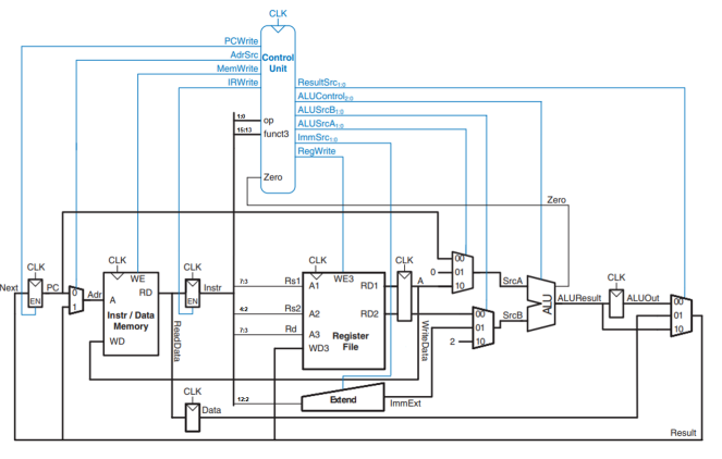
- Schematic of the entire processor. Source: Adapted from e Digital Design and Computer Architecture - RISC-V Edition (Sarah Harris and David Harris)
The above schematic is a modified version of the schematic found on the referenced book and consists on an adapted version of a multi-cycle RISC-V architecture. The identified modules are:
- Control Unit: it's based on a Finite State Machine(FSM) that sends all control signal to the other modules. Its description can be found on the Control Unit page.
- Arithmetical Logic Unit(ALU): performs all the implemented arithmetical operation on hardware. Its description can be found on the ALU page
- Register File: It's a bank of registers that holds data for the processor("closer" than the memory) and can be operated on via the instructions. Its description can be found on the Registers and Register Bank page.
- Other registers: There are some other registers distributed through the processor, such as the Program Counter, that have a specific role and cannot be directly accessed via instructions. Their description can be found on the Registers and Register Bank page
- Instr/Data Memory: consists on the instruction or data memory accessed by the processor. It is not implemented here, since the internal memory from the FPGA kit is used(being so, it also does not have a documentation page on this wiki).
- Extend: The extend module, called here immediate module, parses the different immediate options on the different possible instructions. Its description can be found along on the Control Unit page
- Muxes: There are also some muxes distributed along the schematic, that choose between specific signals to a same wire based on a control signal. It is not documented on a specific page because it is not implemented by a specific module, but rather it's behavior of choosing between signals is replicated on Verilog syntax.(Just for instance, a implementation of a MUX as module can be found inside ALU documentation, since it was chosen to implement the internal muxes of ALU like this. These external ones present on the Golden Top module are not implemented like this.)
Being so, it is easy to see that the role of the Golden Top module is to instantiate and wire all the modules as specified on the schematic and provide debug features for the whole project. The signal's role on each module becomes clear once each description is well understood, so it will not be repeated here. For the modules that have no dedicated page description, the signals are pretty trivial: the memory has a input adress and output data, but also a clock signal and a write enable to distinguish between read and write; the muxes simply have a control signal, many input signals and a output signal.
The notation for the drawn modules on the schematic do not differ from the conventions of digital systems and computer architecture and should also be well understood.
Code organization and description
The file DE10_Lite_Golden_Top.v contains the "Golden Top" top module.
The module's organization is described bellow:
After module's header declaration, the wires and intern registers are declared.
...
wire clk;
wire reset;
wire clkn;
wire [25:0] clk_cnt;

wire [3:0] num_state;

//Internal signals
reg [15:0] PC;
wire [15:0] Adr;
reg [15:0] Instr;
...
Then the Finite State Machine - the Control Unit - is declared
...
//Unit Control
control_unit FSM0
(
	// Inputs
	.clk(clk),
	.reset(reset),
	.zero_flag(Zero),
	.instruction(Instr),
	// Outputs
	.pc_write(PCWrite),
	...
...
Followed by the program counter behavior definition
...
//PC Register
always @ (posedge clk or posedge reset)
begin
	if (reset)
		PC <= 0;
	else if (PCWrite)
		PC <= Result;
end
...
and the definition of the Memory Address source selection.
...
//Memory Address source selection
assign Adr = AdrSrc ? Result : PC;
...
To implement the Program/Data Memory - the System's RAM - a .mif file was used to describe the initial state of the RAM after programming the FPGA. So, the module declaration on the golden top follows:
...
//Program/Data Memory
DE10_LITE_Memory Memory0(
	.address({1'b0, Adr[10:1]}),
	.clock(clkn),
	.data(WriteData),
	.wren(MemWrite),
	.q(ReadData)
);
...
The Instruction Register and Data Register behavior definition follows the previous definition:
- Instruction register (IR)
...
//IR Register
always @ (posedge clk)
begin
	if (IRWrite)
		Instr <= ReadData;
end
...
- Data register
...
//Data Register
always @ (clk)
begin
	Data <= ReadData;
end
...
Register Bank declaration
...
//Register Bank
RegBank #(.WIDTH(16),.SIZE(3)) RegBank0(
	//Entradas
	.clk(clk),
	.we3(RegWrite),
	.A1(Rs1),
	...
	// Saidas
	.RD1(RD1),
	.RD2(RD2)
);
...
Immediate handler declaration and definition
...
//Imm source selection
assign ImmExt = (ImmSrc == 2'b00) ?
	{
		{
			Imm8U[4], Imm8U[4], Imm8U[4], Imm8U[4],
			Imm8U[4], Imm8U[4], Imm8U[4], Imm8U[4]
		}
		, Imm8U
		, Imm8D
	} :	// Signal extended
...
Register Data section
...
//Reg Data
always @ (posedge clk)
begin
	WriteData <= RD1;
	B <= RD2;
end
...
Finally, the section of ALU, that means the declaration and the Input/Output selection behavior definition:
//ALU A source selection
assign SrcA =	(ALUSrcA == 2'b00) ? PC :
		(ALUSrcA == 2'b01) ? 16'b0 :
		(ALUSrcA == 2'b10) ? WriteData :
		16'b0;
...
ALU #(.WIDTH(16)) ALU0
(
	//Entradas
	.SrcA(SrcA),
	.SrcB(SrcB),
	.ALUControl(ALUControl),
	//Saidas
	.ALUResult(ALUResult),
	.zero(Zero)
);
...
And then the System Counter declaration
...
DE10_LITE_counter #(.WIDTH(26)) CNT0
(
	.clk(MAX10_CLK1_50),
	.clr(1'b0),	//Free running
	.q(clk_cnt)
);
...
Debug features
Additionally, the project has Debug features such as VGA and seven segment display support, showing registers and system status. Specifically, the VGA displays full information of the CPU status: flags' state, registers current data, current state of the control unit and etc.
...
DE10_LITE_decod display1
(
	PC[3], PC[2], PC[1], PC[0],
	HEX1[0], HEX1[1], HEX1[2], HEX1[3], HEX1[4],
	HEX1[5], HEX1[6]//, //HEX1(7)
);
...
DE10_LITE_VGA_Generator VGA0
(
	.MAX10_CLK1_50(MAX10_CLK1_50),
        .KEY(KEY),
	.SW(SW),
        .VGA_R(VGA_R),
...