RH11 Massbus Controller - KS10FPGA/KS10FPGA GitHub Wiki
In-essence, the RH11 is a Unibus to Massbus bus bridge.
The KS10 FPGA includes one or two RH11 Massbus Controllers - depending on how the KS10 FPGA is configured. In the KS10 system, one RH11 is attached to the UBA1 Unibus Bridge and provides a Massbus interface to up 8 Disk Drives. A optional second RH11 is attached to UBA3 and provides a Massbus interface to up to 8 Tape Controllers (or Tape Formatters).
There were several variants of the RH11; most of them were intended for use in PDP-11 systems. Of these variants, the RH11-C was created for use in the KS10 and uses the M9724-YA card which adds a Unibus "Bus Hog" mode (enabled by a jumper) that greatly improves the performance of Disk Drives. In "Bus Hog" mode, the RH11-C can do unarbitrated Unibus block transfers. Normally, the RH11-C that interfaces with the Disk Drives is configured for "Bus Hog" mode while the RH11-C that is controlling the Tape Drives is not configured for "Bus Hog" mode. Note: when the RH11-C is configured in "Bus Hog" mode, the RH11-C can be the only peripheral device attached to that Unibus since the DMA (or as DEC call it: "NPR") operations are unarbitrated.
The KS10 FPGA always arbitrates IO Bus accesses; therefore this "Bus Hog" mode is not implemented.
Lastly, the KS10 FPGA "Massbus" implementation looks nothing like the DEC "Massbus". The KS10 FPGA implementation is a 36-bit wide synchronous bus that is similar to the KS10 Backplane Bus and the KS10 FPGA IO Bus implementation.
The following RH11 documentation is available:
- RH11-B Engineering Drawings (Schematic), Rev A, 1977
- RH11-C Engineering Drawings (Schematic), Rev A, 1977
- RH11-A, RH11-B Engineering Drawings (Schematic), Rev J, 1978
- RH11-A, RH11-B Engineering Drawings (Schematic), Rev K, 1978
- RH11-A, RH11-B Option Description, Rev B, 1979
- RH11 Peripheral Controller Course Documents, 1979
- RH11/RH70 Massbus Controllers - A Self-Paced Course, 1979
The RH11 FPGA implementation is fully parameterized and may be configured as follows:
RH11 Configuration |
|||||
Device |
UBA |
Interrupt |
Interrupt |
Base |
Use |
RH11 #1 |
UBA1 |
6 |
000254 |
776700 |
Disk Controller |
RH11 #3 |
UBA3 |
6 |
000224 |
772440 |
Tape Controller |
The Massbus Interface between the RH11 and the disk and tape devices is implemented as a SystemVerilog 'interface' which encapsulates the Massbus signals. This interface does support both disk drives and tape drives.
The RH11 Massbus Controller exposes two different types of registers to the programmer:
- Controller Registers that are located in the RH11 Massbus Controller that apply to all disk/tape drives, and
- Device Registers that are located inside the individual disk/tape drives and apply only to that device.
In a real KS10, the Controller Registers were part of the RH11 Controller and the Device Registers were located in the disk drives or tape drives on the device side of the Massbus cabling. This hierarchy is maintained in the KS10 FPGA although the Massbus cabling is more a logical concept than a physical implementation.
The RH11 Massbus Controller maintains state and reports status that is applicable to the entire Massbus system. For example the Controller RPCS2 register has 3 bits which select which of the 8 disk/tape devices is addressed to receive commands or report status. That controller state includes the following registers:
RH11 Controller Register Summary |
|||
Unibus |
Register |
R/W |
Register Description |
|
R/W |
Control and Status Register #1 Portions of this register are in the RH11. Portions of this register are in the Massbus device and vary by device. |
|
776702 |
R/W |
Word Count Register |
|
776704 |
R/W |
Bus Address Register |
|
776710 |
R/W |
Control and Status Register #2 |
|
776722 |
R/W |
Data Buffer Register |
|
The Massbus register are mapped at various locations in the RH11 address space. In implementation, a ROM maps IO Bus addresses (Unibus) to Massbus addresses.
The exact details of Massbus registers depend on the types of devices that are attached to the Massbus - the RH11 just passes the Massbus registers through the RH11 interface. Note: RPxx disk drives are different that RMxx disk drives; and tape drives are different than disk drives.
The Massbus Register addresses are summarized below.
Massbus Register Address Cross Reference |
||||
Reg # (octal) |
RP Register Name |
RM Register Name |
TU Register Name |
Comment |
0 |
RPCS1 |
RMCS1 |
MTCS1 |
Compatible between RP, RM, and TU. |
1 |
RPDS |
RMDS |
MTDS |
Compatible between RP, RM, and TU. |
2 |
RPER1 |
RMER1 |
MTER |
Compatible between RP, RM, and TU. |
3 |
RPMR |
RMMR1 |
MTMR |
Compatible between RP, RM, and TU. |
4 |
RPAS |
RMAS |
- |
|
5 |
RPDA |
RMDA |
MTFC |
|
6 |
RPDT |
RMDT |
MTDT |
Compatible between RP, RM, and TU. |
7 |
RPLA |
RMLA |
MTCC |
|
10 |
RPSN |
RMSN |
MTSN |
Compatible between RP, RM, and TU. |
11 |
RPOF |
RMOF |
MTTC |
|
12 |
RPDC |
RMDC |
- |
|
13 |
RPCC |
RMHR |
- |
RMHR is read-write whereas RPCC is read-only. |
14 |
RPER2 |
RMMR2 |
- |
RPER2 and RMER2 are compatible since neither is implemented. |
15 |
RPER3 |
RMER2 |
- |
RPER3 and RMER2 are compatible since neither is implemented. The RMER2 is read-only but maybe nobody will notice. |
16 |
RPEC1 |
RMEC1 |
- |
|
17 |
RPEC2 |
RMEC2 |
- |
|
This register provides high level control and status of the disk/tape system.
This register may be accessed as a byte or a word.

Control and Status #1 Register (RHCS1)
|
RH11 Control and Status Register #1 (RHCS1) – IO Address 776700 |
|||
Bit(s) |
Mnemonic |
R/W |
Description |
15 |
SC |
R |
Special Conditions SC is asserted under the following conditions:
SC is combinatorially derived from those registers – clearing that register will clear SC. This will cause an interrupt if Ready (RHCS1[RDY]) is also asserted. |
14 |
TRE |
R/W |
Transfer Error TRE is asserted when any of the following bits transition to asserted:
TRE is negated by:
Note: These transitions are not detected independently. The big “OR” comes before the edge detection – not after. |
13 |
CPE |
R |
Controller Bus Parity Error A CPE is created by a Massbus device that is sending incorrect parity on the Massbus Control Bus to the RH11. The KS10 FPGA does not implement parity on Massbus, so the Massbus devices simply force parity errors. CPE is asserted by:
CPE is negated by:
Writes ignored. Apparently an RP-type Disk Drives cannot generate intentionally incorrect parity to test the RH11. |
12 |
- |
R |
Reserved Writes ignored. Always read as zero. |
11 |
DVA |
R |
Drive Available. See device. |
10 |
PSEL |
R/W |
Port Select Not implemented. PSEL is asserted by writing to '1' to PSEL when ready (RHCS1[RDY] = '1'). PSEL is negated when:
|
9-8 |
A[17:16] |
R/W |
Address Extension Bits. See RHBA Register. A[17:16] may be modified by writing when ready (RHCS1[RDY] asserted). A[17:16] is incremented as part of the RHBA register. A[17:16] is negated when:
|
7 |
RDY |
R |
Ready RDY is negated when a command starts execution. RDY is asserted when:
|
6 |
IE |
R/W |
Interrupt Enable IE is asserted by writing a '1' to IE. IE is negated by:
Note: Asserting RHCS1[RDY] and IE simultaneously causes an immediate interrupt. |
5-1 |
FUN |
R/W |
Function See device. |
0 |
GO |
R/W |
GO See device. |
The program loads the RPWC Register with the two-complement number of the words to be read from or written to the disk/tape drive.
Each time a 36-bit word is transferred, the word count is incremented by two.
Disks always read and write full sectors. On writes, partial sectors are filled with zero.
Tapes always transfer an even number of words.
This register may be accessed as a byte or a word.

RH11 Word Count Register (RHWC)
RH11 Word Count Register (RHWC) – IO Address 776702 |
|||
Bit(s) |
Mnemonic |
R/W |
Description |
15-0 |
WC |
R/W |
Word Count WC is altered by writing and increments by two each time a 36-bit word is read from or written to the disk/tape drive. When the disk/tape drive has completed reading or writing data, the register contents should be zero. There is no reset mechanism. |
The Bus Address register contains the virtual address of the source memory for writes or the virtual address of the destination memory for reads.
For forward operations, the program loads the starting address. Each time a 36-bit word is transferred, the address is incremented by two.
For reverse operations, the program loads the ending address. Each time a 36-bit word is transferred, the address is decremented by two.
This register may be accessed as a byte or a word.
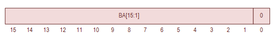
RH11 Bus Address Register (RPBA)
RH11 Bus Address Register (RHBA) – IO Address 776704 |
|||
Bit(s) |
Mnemonic |
R/W |
Description |
15-1 |
BA[15:1] |
R/W |
Bus Address. See also RHCS1[A17:A16]. BA is altered by writing If Bus Address Increment Inhibit (RHCS2[BAI]) is negated:
BA[17:1] is cleared by:
The disk controller and tape controller is hardwired to only transfer 36-bit words to/from memory. The address increment described above is consistent with the 36-bit transfer. Note: Only tape drives perform reverse operations. Don't attempt a reverse operation on a disk drive. |
0 |
BA[0] |
R |
Bus Address (Bit 0) Writes ignored. Always read as zero. |
This register indicates the status of the controller.
This register may be written as a byte or a word.

RH11 Control and Status Register #2 (RHCS2)
RH11 Control and Status Register #2 (RHCS2) – IO Address 776710 |
|||
Bit(s) |
Mnemonic |
R/W |
Description |
15 |
DLT |
R |
Device Late DLT is asserted under the following conditions:
Otherwise the DLT is not implemented as far as disk/tape operation is concerned. Disk/tape data bypasses the SILO. DLT is negated by:
|
14 |
WCE |
R |
Write Check Error WCE is asserted by the Write Check Command when the data read from disk/tape does not match the data read from memory. WCE is negated by:
|
13 |
UPE |
R/W |
Unibus Parity Error UPE is asserted by writing a '1' to UPE. UPE is negated by:
|
12 |
NED |
R |
Non-existent Drive NED is asserted by reading or writing to a drive that is not present. NED is negated by:
|
11 |
NEM |
R |
Non-existent Memory NEM is asserted by reading or writing to memory that is not present. NEM is negated by:
|
10 |
PGE |
R |
Program Error PGE is asserted by attempting to execute a command when when the drive is not ready. I.e., asserting RHCS1[GO] with RHCS1[RDY] negated. PGE is negated by:
|
9 |
MXF |
R/W |
Missed Transfer Does nothing. MXF asserting by writing a '1' to MXF. MXF is negated by:
|
8 |
DPE |
R/W |
Data Bus Parity Error DPE is asserted by a Massbus device that is sending incorrect parity on the data bus to the RH11. The KS10 FPGA does not implement parity on Massbus; but the Massbus devices do have a means to perform parity tests. In the KS10 FPGA, instead of this testing parity, this test mode simply forces parity errors. For example, DPE is asserted when a TM02/TM03 Maintenance Register is configured for even parity ((MTMR[MM] = 1) and (MTMR[MOP] = 2)) and a tape read operation is performed. DPE is negated by:
Writes ignored. This is tested by DSTUA TST165. |
7 |
OR |
R |
Output Ready Writes ignored. OR is asserted when the data SILO is not empty. OR is negated when:
|
6 |
IR |
R |
Input Ready Writes ignored. IR is asserted when the data SILO is not full. IR is negated when:
|
5 |
CLR |
W |
Controller Clear Always read as zero. Asserting CLR resets many of the controller registers. When disk drives are attached to the RH11, asserting CLR resets the selected RP/RM disk drive. When tape drives are attached to the RH11, asserting CLR resets the selected TM02/TM03 and resets the selected slave tape drive. It does NOT reset any unselected slave tape drives. |
4 |
PAT |
R/W |
Parity Test PAT is asserted to a Massbus device to verify that the Massbus device can detect parity errors. The KS10 FPGA does not implement parity on Massbus; but asserting this signal wil force a parity error to be detected. For example, asserting PAT and performing a write to a Massbus register will cause MTER[CPAR] or RPER1[CPAR] depending on the Massbus device. PAT is asserted by writing a '1' to PAT. PAT is negated by:
Control bus parity testing on a TM02/TM03 is performed by DSTUA TST6. |
3 |
BAI |
R/W |
Bus Address Increment Inhibit When BAI is asserted, the Bus Address is not incremented or decremented when words are transferred to/from the disk/tape. BAI is asserted by writing a '1' to BAI when the drive is ready (RHCS1[RDY] = '1'). BAI is negated by:
|
2-0 |
UNIT |
R/W |
Unit Select UNIT selects the active disk drive or active tape controller. UNIT is altered by writing to UNIT. UNIT is negated when:
|
The RHDB register interfaces to the data SILO for read and write operations. The disk/tape unit as implemented does not use the data SILO – disk/tape data flows directly between memory and the SD Card; however, the data SILO operation is tested as part of the DSRPA diagnostic program. Therefore the RHDB register and data SILO is implemented as required by that diagnostic. Data can be written to the SILO and read back from the SILO but has no other effect on the disk/tape operation.
The Input Ready flag of the Control and Status #2 (RHCS2[IR]) is asserted when the data SILO is not full. The 66th write to the data SILO after reset should cause the SILO to indicate that the data SILO is full.
The Output Ready flag of the Control and Status #2 (RHCS2[OR]) is asserted when the data SILO is not empty. RHDB is a SILO input/output so I don’t see how it could be byte addressable.
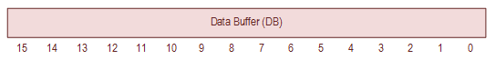
RH11 Data Buffer Register (RPDB)
RH11 Data Buffer Register (RHDB) – IO Address 776722 |
|||
Bit(s) |
Mnemonic |
R/W |
Description |
15-0 |
DB[15:0] |
R/W |
Data Buffer The DB register is only implemented as required to pass certain diagnostic tests. Normally disk/tape data would pass through the DB SILO, but in this implementation, the DB SILO is only for diagnostics. DB is a read/write register that interfaces to the data SILO. Data written to the DB register is pushed into the SILO. Data read from the DB register is popped from the SILO. The SILO is cleared by:
|
The RH11 Interrupt is a strange combination of edge-triggered and level-triggered conditions. For a detailed description of the RH11 interrupt logic, see the paper entitled "PDP-11 Interrupts: Variations On A Theme" by Bob Supnik.
The Interrupt Flip-Flop is set under the following conditions:
- When controller transitions to Ready (RHCSR1[RDY] = '1') with Interrupt Enable asserted (RHCSR[IE] = '1'), or
- When the Control Register #1 (RHCS1) is written with both Interrupt Enable asserted (RHCS1[IE] = '1') and Data Ready asserted (RHCS1[RDY] = '1').
The Interrupt Flip-Flop is cleared by:
- Asserting IO Bridge Clear (UBACSR[INI] = '1'),
- Asserting Controller Clear (RHCS2[CLR] = '1'), or
- Receiving and Interrupt Acknowledge bus cycle that addresses the RH11.
An Interrupt Request is generated under the following conditions:
- The Interrupt Flip-Flop is set per above, or
- Special Conditions (RHCSR1[SC]) and Ready (RHCS1[RDY]) are both set.
The Interrupt Request is negated when the KS10 CPU acknowledges the interrupt.
The RH11 Massbus Controller and RP06 Disk array appears to be working. I built an RP06 Reliability Exerciser and Diagnostic Pack (RED Pack) from the tape image in SIMH and copied the disk image to the Secure Digital (SDHC) Card. To my complete surprise, I can actually navigate around the Tops-20 RP06 Red Pack disk and successfully execute many of the tests successfully. The RED Pack was used to "demonstrate to the customer, the forty-eight hour Hardware Reliability portion of System Acceptance" - so it is a very useful hardware debugging aid. A transcript from the TTY has been captured in the document entitled "Exploring the REDPACK".
The diagnostic status of the RH11 and RP06 is summarized below:
                           DIAGNOSTIC                            Result
---------------------------------------------------------------- ------
DSRPAC0 DECSYSTEM 2020 KS10/RH11 - RP06 BASIC DEVICE DIAGNOSTIC  *Pass
DSRMB   DECSYSTEM 2020 RH11 - RM03/RP06 - RELIABILITY DIAGNOSTIC ????
* This includes expected failures because the RP06 Diagnostic Mode is not implemented. The RP06 Diagnostic Mode is only used by the diagnostic program and is not required for any of the Monitor programs. See DSRPA DECSYSTEM 2020 RP06-RH11 Basic Drive Diagnostic Failure (Issue #8)