KS10 Blackplane Bus - KS10FPGA/KS10FPGA GitHub Wiki
The original DEC KS10 used a tri-state bus for the KS10 backplane. The KS10 FPGA uses a variant of this bus which is suitable for an FPGA implementation. It turns out that the operation this bus is wired into the KS10 microcode and significant design changes to this bus would require changes to the KS10 microcode.
The DEC KS10 backplane bus was implemented using a multiplexed address and data protocol. The address and control information was asserted onto the first of the bus cycles and the data was asserted onto the bus on a later bus cycle. This has been replaced by design with an independent address bus and data bus. This design change increases memory bandwidth with a slight increase in the amount of routing resources that the FPGA requires.
Because most FPGAs don’t support tri-state buses, the backplane is more of a logical notion. In actual implementation, the backplane is more of a big multiplexer than a bus structure.
The KS10 FGPA backplane supports multiple initiators and multiple targets. The bus is arbitrated on a cycle-by-cycle basis. This simplifies the bus implementation.
The Bus Arbiter Operations are summarized below:
Bus Arbiter Operations |
|||
Device |
Initiator |
Target |
Priority |
CPU |
Yes |
No |
Lowest |
Console |
Yes |
Yes |
Middle |
Memory Controller |
No |
Memory Only |
N/A |
IO Bridge #1 |
Yes |
Yes |
Highest |
IO Bridge #3 |
Yes |
Yes |
Highest |
IO Bridge #4 |
Yes |
Yes |
Highest |
A block diagram of the KS10 FPGA illustrating the KS10 Backplane Bus with peripherals installed is shown below:

KS10 FPGA Block Diagram
The KS10 FPGA address bus contains control flags in the upper bits and address in the lower bits. Although the control flags aren’t technically part of the address, they are often decoded with the address and this paradigm nicely simplifies the bus design.
The DEC KS10 uses a slightly different format for the bus control signals than the DEC KS10. The KS10 FPGA uses the standard VMA layout for the bus control signals and relies on the Verilog optimizer to remove the unused signals.
The address and control ‘flags’ are defined as follows

Address Bus Definition
Address Flag Definitions |
|||
Bit |
Mnemonic |
Description |
|
0 |
USER |
User Mode |
|
1 |
EXEC |
Exec Mode |
|
2 |
FETCH |
Instruction Fetch |
|
3 |
READ |
Read Cycle |
|
4 |
WRTEST |
When WRTEST is asserted, this will create a page fault on a virtual memory page that is not writeable. |
|
5 |
WRITE |
Write Cycle |
|
6 |
EXTENDED |
Extended Address Cycle |
|
7 |
CACHEINH |
Cache Inhibit |
|
8 |
PHYSICAL |
Physical Address |
|
9 |
PREVIOUS |
VMA Previous Context |
|
10 |
IO |
IO Cycle |
|
11 |
WRU |
Who Are You |
|
UBA |
IDENTIFIER |
||
UBA0 |
36'o000000_400000 |
||
UBA1 |
36'o000000_200000 |
||
UBA2 |
36'o000000_100000 |
||
UBA3 |
36'o000000_040000 |
||
UBA4 |
36'o000000_020000 |
||
|
If no device responds to this request, the microcode assumes that the CPU's APR has requested the interrupt. |
|||
12 |
VECTOR |
Read Interrupt Vector from UBA |
|
13 |
IOBYTE |
IO BYTE |
|
The KS10 FPGA data bus always provides 36-bit data between the source and destination.
Memory read cycles are always 36-bit bus cycles with a 20-bit address.
Memory Read Cycles always assert READ (bit 3), negate WRITE (bit 5), and negate IO (bit 10).
If PHYSICAL (bit 8) is asserted, this address refers to a physical address (one of the ACs, for example) instead of a virtual (memory) address.
If FETCH (bit 2) is asserted, this is an instruction fetch.

Memory Write Cycles always assert WRITE (bit 5), negate READ (bit 3), and negate IO (bit 10).
If PHYSICAL (bit 8) is asserted, this address refers to a physical address (one of the ACs, for example) instead of a virtual address (memory).
If WRTEST (bit 4) is also asserted, the PAGER will also test the address for a non-writable page access violation.

The KS10 FPGA IO Bus is implemented quite a bit different than the DEC KS10 Unibus. Whereas the DEC Unibus was limited to 16-bit registers and in some cases 18-bit NPR data (the RH11 is 18-bit), the IO Bus in the KS10 FPGA is more like an extension of the KS10 Backplane bus where the 36-bit address and a 36-bit data is arbitrated and bridged by the UBA. This greatly increases the bandwidth of the IO operations.
From a hardware point of view, IO Read operations are always 36-bit and can transfer 36-bit data, 16-bit data, or 8-bit data.
The Memory Status Register (address o100000) is an example of a 36-bit IO register.
When a 16-bit or 8-bit Unibus register read, the device right justifies the 16-bit data (reads are always 16-bit)
and pads the upper 20 data bits with zero.
For 8-bit reads, the CPU microcode masks and shifts the 16-bit data as required to select the proper 8-bit byte.
Similarly, IO Write operations are always 36-bit and can transfer 36-bit data, 16-bit data, or 8-bit data.
When a 16-bit or 8-bit Unibus register written, the device truncates the upper 20-bits of data and is left with 16-bit, right justified data.
The IO BYTE bit and the LSB of the address can be used to select either or both byte-lanes for writing.
Word IO Read Cycles always assert READ (bit 3), negate WRITE (bit 5), assert PHYSICAL (bit 8), assert IO (bit 10), and negate IO BYTE (bit 13). The hardware register size (and padding) determines whether 36-bit or 16-bit data is read.

Word IO Read Cycles always assert READ (bit 3), negate WRITE (bit 5), assert PHYSICAL (bit 8), assert IO (bit 10), and assert IO BYTE (bit 13).
When B is negated (Address bit 35), the low byte is read.
When B is asserted (Address bit 35), the high byte is read.

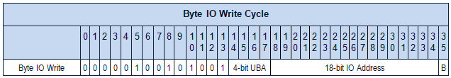
Word IO Write Cycles always negate READ (bit 3), assert WRITE (bit 5), assert PHYSICAL (bit 8), assert IO (bit 10), and negate IO BYTE (bit 13). The hardware register size determines whether 36-bit or 16-bit data is written.

Word IO Write Cycles always negate READ (bit 3), assert WRITE (bit 5), assert PHYSICAL (bit 8), assert IO (bit 10), and assert IO BYTE (bit 13).
When B is negated (Address bit 35), the low byte is written.
When B is asserted (Address bit 35), the high byte is written.
The WRU Cycle is an IO READ bus cycle that to determine which UBA, if any, is currently requesting an interrupt.
WRU Cycles always assert READ (bit 3), negate WRITE (bit 5), assert PHYSICAL (bit 8), assert IO (bit 10), and assert WRU (bit 11).
The address bits (ADDR[18:0]) are ignored and the requested PI Level is asserted onto PI bits (ADDR[15:17]).

Vector Cycles always assert READ (bit 3), negate WRITE (bit 5), assert PHYSICAL (bit 8), assert IO (bit 10), and assert VECT (bit 12).
The address bits (ADDR[18:0]) are ignored and the requested UBA number is asserted onto UBA # bits (ADDR[14:17]).

The interrupt sequence is as follows:
- The IO Device asserts one of the Device Interrupt Request (devINTR[7:4]) signals.
- The IO Bus Bridge “ORs” the Device Interrupt Request signals (devINTR[7:4]) from each of the IO Devices together.
Next the IO Bus Bridge maps the Device Interrupt Request signals to one of the 7 CPU interrupt request priorities
using the High Priority and Low Priority register settings in the IO Bus Bridge Control and Status Register.
The CPU Interrupt signals are asserted on the busINTR[1:7] pins of the Backplane Bus.
See the Priority Interrupt High (PIH) and the Priority Interrupt Low (PIL) bits of the UBA Status Register (UBACSR) for more information on how this interrupt priority mapping occurs. - The Backplane Bus Arbiter “ORs” together the External Priority Interrupt signals from each of the IO Bus Bridges and sends the result to the Priority Interrupt Controller inside CPU.
- The Priority Interrupt Controller inside the CPU selects the highest priority interrupt and interrupts the CPU by asserting the “pageFAIL” signal. The CPU microcode eventually notices that the “pageFAIL” signal is asserted and dispatches to the interrupt processing microcode. There, the CPU issues a Who Are You (WRU) bus cycle with the interrupt priority that is being handled.
- All the IO Bus Bridges receive the WRU bus cycle and each IO Bus Bridge compares the interrupt priority associated with the WRU with the interrupt priority it may be asserting. If the priority of the WRU bus cycle matches the priority of the IO Bus Bridge, the IO Bus Bridge responds with its WRU identifier response.
- It is possible that more than one IO Bus Bridge is asserting the same interrupt. If so, the KS10 Backplane
Bus Arbiter selects the highest priority IO Bus Bridge’s WRU response.
Note: the lowest UBA number is the highest priority IO Bus Bridge. - It is also possible that more than one device attached to the IO Bus Bridge is asserting that same interrupt request. For the purpose of WRU bus cycle, this is irrelevant. This will be resolved later during the Interrupt Vector Cycle.
- The microcode in the CPU examines the identifier that is received, if any. If no identifier is received, the CPU handles the interrupt as an APR interrupt. If an identifier is received, the CPU performs an Interrupt Vector bus cycle which is addressed to the IO Bus Bridge that was associated with the WRU identifier that was arbitrated and received by the CPU.
- The addressed IO Bus Bridge arbitrates the the Interrupt Vector bus cycle to the highest priority device that is asserting
the highest priority interrupt; but note, the interrupt priority selection occurs before the device selection.
The selected device responds with its associated Interrupt Vector and the IO Bridge forwards the Interrupt Vector back to the CPU.
The device uses the Interrupt Vector bus cycle as an Interrupt Acknowledge indication.
Note: as an implementation detail, the timing of the Interrupt Acknowledge with respect to the Interrupt Vector bus cycle is important:- If the interrupt clears during the Interrupt Vector bus cycle, the interrupt vector will be misread by the microcode.
- If the interrupt clears much after the Interrupt Vector bus cycle is complete, the interrupt will be recognized twice.
- The CPU software handles the interrupt as described by the KS10 Architecture.